EP3650937B1 - Appareil d'impression et procédé de fabrication d'un produit - Google Patents
Appareil d'impression et procédé de fabrication d'un produit Download PDFInfo
- Publication number
- EP3650937B1 EP3650937B1 EP19205896.4A EP19205896A EP3650937B1 EP 3650937 B1 EP3650937 B1 EP 3650937B1 EP 19205896 A EP19205896 A EP 19205896A EP 3650937 B1 EP3650937 B1 EP 3650937B1
- Authority
- EP
- European Patent Office
- Prior art keywords
- light
- substrate
- mold
- imprint
- modulated
- Prior art date
- Legal status (The legal status is an assumption and is not a legal conclusion. Google has not performed a legal analysis and makes no representation as to the accuracy of the status listed.)
- Active
Links
Images




Classifications
-
- G—PHYSICS
- G03—PHOTOGRAPHY; CINEMATOGRAPHY; ANALOGOUS TECHNIQUES USING WAVES OTHER THAN OPTICAL WAVES; ELECTROGRAPHY; HOLOGRAPHY
- G03F—PHOTOMECHANICAL PRODUCTION OF TEXTURED OR PATTERNED SURFACES, e.g. FOR PRINTING, FOR PROCESSING OF SEMICONDUCTOR DEVICES; MATERIALS THEREFOR; ORIGINALS THEREFOR; APPARATUS SPECIALLY ADAPTED THEREFOR
- G03F7/00—Photomechanical, e.g. photolithographic, production of textured or patterned surfaces, e.g. printing surfaces; Materials therefor, e.g. comprising photoresists; Apparatus specially adapted therefor
- G03F7/0002—Lithographic processes using patterning methods other than those involving the exposure to radiation, e.g. by stamping
-
- G—PHYSICS
- G03—PHOTOGRAPHY; CINEMATOGRAPHY; ANALOGOUS TECHNIQUES USING WAVES OTHER THAN OPTICAL WAVES; ELECTROGRAPHY; HOLOGRAPHY
- G03F—PHOTOMECHANICAL PRODUCTION OF TEXTURED OR PATTERNED SURFACES, e.g. FOR PRINTING, FOR PROCESSING OF SEMICONDUCTOR DEVICES; MATERIALS THEREFOR; ORIGINALS THEREFOR; APPARATUS SPECIALLY ADAPTED THEREFOR
- G03F7/00—Photomechanical, e.g. photolithographic, production of textured or patterned surfaces, e.g. printing surfaces; Materials therefor, e.g. comprising photoresists; Apparatus specially adapted therefor
- G03F7/16—Coating processes; Apparatus therefor
- G03F7/168—Finishing the coated layer, e.g. drying, baking, soaking
-
- G—PHYSICS
- G03—PHOTOGRAPHY; CINEMATOGRAPHY; ANALOGOUS TECHNIQUES USING WAVES OTHER THAN OPTICAL WAVES; ELECTROGRAPHY; HOLOGRAPHY
- G03F—PHOTOMECHANICAL PRODUCTION OF TEXTURED OR PATTERNED SURFACES, e.g. FOR PRINTING, FOR PROCESSING OF SEMICONDUCTOR DEVICES; MATERIALS THEREFOR; ORIGINALS THEREFOR; APPARATUS SPECIALLY ADAPTED THEREFOR
- G03F7/00—Photomechanical, e.g. photolithographic, production of textured or patterned surfaces, e.g. printing surfaces; Materials therefor, e.g. comprising photoresists; Apparatus specially adapted therefor
- G03F7/20—Exposure; Apparatus therefor
- G03F7/2051—Exposure without an original mask, e.g. using a programmed deflection of a point source, by scanning, by drawing with a light beam, using an addressed light or corpuscular source
- G03F7/2057—Exposure without an original mask, e.g. using a programmed deflection of a point source, by scanning, by drawing with a light beam, using an addressed light or corpuscular source using an addressed light valve, e.g. a liquid crystal device
-
- G—PHYSICS
- G03—PHOTOGRAPHY; CINEMATOGRAPHY; ANALOGOUS TECHNIQUES USING WAVES OTHER THAN OPTICAL WAVES; ELECTROGRAPHY; HOLOGRAPHY
- G03F—PHOTOMECHANICAL PRODUCTION OF TEXTURED OR PATTERNED SURFACES, e.g. FOR PRINTING, FOR PROCESSING OF SEMICONDUCTOR DEVICES; MATERIALS THEREFOR; ORIGINALS THEREFOR; APPARATUS SPECIALLY ADAPTED THEREFOR
- G03F7/00—Photomechanical, e.g. photolithographic, production of textured or patterned surfaces, e.g. printing surfaces; Materials therefor, e.g. comprising photoresists; Apparatus specially adapted therefor
- G03F7/70—Microphotolithographic exposure; Apparatus therefor
- G03F7/70058—Mask illumination systems
- G03F7/70091—Illumination settings, i.e. intensity distribution in the pupil plane or angular distribution in the field plane; On-axis or off-axis settings, e.g. annular, dipole or quadrupole settings; Partial coherence control, i.e. sigma or numerical aperture [NA]
- G03F7/70116—Off-axis setting using a programmable means, e.g. liquid crystal display [LCD], digital micromirror device [DMD] or pupil facets
-
- G—PHYSICS
- G03—PHOTOGRAPHY; CINEMATOGRAPHY; ANALOGOUS TECHNIQUES USING WAVES OTHER THAN OPTICAL WAVES; ELECTROGRAPHY; HOLOGRAPHY
- G03F—PHOTOMECHANICAL PRODUCTION OF TEXTURED OR PATTERNED SURFACES, e.g. FOR PRINTING, FOR PROCESSING OF SEMICONDUCTOR DEVICES; MATERIALS THEREFOR; ORIGINALS THEREFOR; APPARATUS SPECIALLY ADAPTED THEREFOR
- G03F7/00—Photomechanical, e.g. photolithographic, production of textured or patterned surfaces, e.g. printing surfaces; Materials therefor, e.g. comprising photoresists; Apparatus specially adapted therefor
- G03F7/70—Microphotolithographic exposure; Apparatus therefor
- G03F7/70058—Mask illumination systems
- G03F7/70191—Optical correction elements, filters or phase plates for controlling intensity, wavelength, polarisation, phase or the like
-
- G—PHYSICS
- G03—PHOTOGRAPHY; CINEMATOGRAPHY; ANALOGOUS TECHNIQUES USING WAVES OTHER THAN OPTICAL WAVES; ELECTROGRAPHY; HOLOGRAPHY
- G03F—PHOTOMECHANICAL PRODUCTION OF TEXTURED OR PATTERNED SURFACES, e.g. FOR PRINTING, FOR PROCESSING OF SEMICONDUCTOR DEVICES; MATERIALS THEREFOR; ORIGINALS THEREFOR; APPARATUS SPECIALLY ADAPTED THEREFOR
- G03F7/00—Photomechanical, e.g. photolithographic, production of textured or patterned surfaces, e.g. printing surfaces; Materials therefor, e.g. comprising photoresists; Apparatus specially adapted therefor
- G03F7/70—Microphotolithographic exposure; Apparatus therefor
- G03F7/70216—Mask projection systems
- G03F7/70283—Mask effects on the imaging process
- G03F7/70291—Addressable masks, e.g. spatial light modulators [SLMs], digital micro-mirror devices [DMDs] or liquid crystal display [LCD] patterning devices
-
- G—PHYSICS
- G03—PHOTOGRAPHY; CINEMATOGRAPHY; ANALOGOUS TECHNIQUES USING WAVES OTHER THAN OPTICAL WAVES; ELECTROGRAPHY; HOLOGRAPHY
- G03F—PHOTOMECHANICAL PRODUCTION OF TEXTURED OR PATTERNED SURFACES, e.g. FOR PRINTING, FOR PROCESSING OF SEMICONDUCTOR DEVICES; MATERIALS THEREFOR; ORIGINALS THEREFOR; APPARATUS SPECIALLY ADAPTED THEREFOR
- G03F9/00—Registration or positioning of originals, masks, frames, photographic sheets or textured or patterned surfaces, e.g. automatically
- G03F9/70—Registration or positioning of originals, masks, frames, photographic sheets or textured or patterned surfaces, e.g. automatically for microlithography
- G03F9/7003—Alignment type or strategy, e.g. leveling, global alignment
- G03F9/7042—Alignment for lithographic apparatus using patterning methods other than those involving the exposure to radiation, e.g. by stamping or imprinting
-
- G—PHYSICS
- G03—PHOTOGRAPHY; CINEMATOGRAPHY; ANALOGOUS TECHNIQUES USING WAVES OTHER THAN OPTICAL WAVES; ELECTROGRAPHY; HOLOGRAPHY
- G03F—PHOTOMECHANICAL PRODUCTION OF TEXTURED OR PATTERNED SURFACES, e.g. FOR PRINTING, FOR PROCESSING OF SEMICONDUCTOR DEVICES; MATERIALS THEREFOR; ORIGINALS THEREFOR; APPARATUS SPECIALLY ADAPTED THEREFOR
- G03F9/00—Registration or positioning of originals, masks, frames, photographic sheets or textured or patterned surfaces, e.g. automatically
- G03F9/70—Registration or positioning of originals, masks, frames, photographic sheets or textured or patterned surfaces, e.g. automatically for microlithography
- G03F9/7065—Production of alignment light, e.g. light source, control of coherence, polarization, pulse length, wavelength
-
- H—ELECTRICITY
- H10—SEMICONDUCTOR DEVICES; ELECTRIC SOLID-STATE DEVICES NOT OTHERWISE PROVIDED FOR
- H10P—GENERIC PROCESSES OR APPARATUS FOR THE MANUFACTURE OR TREATMENT OF DEVICES COVERED BY CLASS H10
- H10P76/00—Manufacture or treatment of masks on semiconductor bodies, e.g. by lithography or photolithography
Definitions
- the present invention relates to an imprint apparatus and a product manufacturing method.
- Japanese Patent Application Laid-Open No. 2013-069918 discusses an imprint apparatus that drips a resist onto a pattern formation region of a substrate, pushes a template against the resist, emits light onto a light irradiated region including a boundary between the pattern formation region and an outer region of the pattern formation region, and then, emits light onto the pattern formation region. By the light emission onto the light irradiated region, the resist on the light irradiated region cures, and the resist is prevented from entering the pattern formation region.
- Japanese Patent Application Laid-Open No. 2013-102132 discusses an imprint apparatus including a heating mechanism that deforms a pattern region of a substrate by heating, and a shape correcting mechanism that deforms a pattern region of a mold.
- Japanese Patent Application Laid-Open No. 2013-102132 discusses that a digital mirror device is used as a unit of forming a heat distribution.
- US 2018/149969 A1 discloses a heating mechanism in an imprint apparatus that changes the shape of a substrate by irradiating a shot area.
- WO 2017/110032 A1 discloses an imprint apparatus comprising a heat release member, a chuck and a curing device.
- WO 2015/111739 discloses an imprint apparatus with a heating unit deforming a shot region by irradiating the shot region with light.
- US 2018/301331 A1 discloses correcting the shape of a pattern region on a substrate by using a heating unit including a digital mirror device or improving the positioning accuracy of the substrate and a mold by increasing the viscosity of the uncured imprint material.
- various devices can be disposed above a mechanism that holds and drives a mold.
- devices such as a curing unit for curing imprint material on a substrate, a deformation unit for deforming the substrate by emitting light onto the substrate, and a detection system for detecting relative positions of the substrate and the mold can be disposed. Because a region for disposing these devices is finite, it has been very difficult to dispose various devices. In addition, if various devices are disposed, the size of the apparatus might increase.
- an imprint apparatus as specified in claims 1 to 19.
- a product manufacturing method as specified in claim 20.
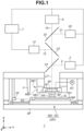
- Fig. 1 illustrates a configuration of an imprint apparatus 1 according to an exemplary embodiment of the present invention.
- the imprint apparatus 1 executes imprint processing and thereby forms a pattern on a substrate S.
- the pattern is made of cured material obtained by curing imprint material IM.
- the imprint processing includes a contact process of bringing the imprint material IM on the substrate S and a mold M into contact with each other, an alignment process of performing alignment of the substrate S and the mold M after the contact process, and a curing process of curing the imprint material IM after the alignment process.
- a curable composition (which may be also referred to as an uncured-state resin) that cures when curing energy is applied thereto is used as the imprint material IM.
- the curing energy include electromagnetic waves and heat.
- electromagnetic waves light, such as infrared light, visible light, and ultraviolet light, that has a wavelength selected from the range of 10 nm or more and 1 mm or less, for example, is used.
- the curable composition is a composition that cures by being irradiated with light or being heated.
- a photocurable composition that cures by being irradiated with light at least contains a polymerizable compound and a photopolymerization initiator, and may contain a nonpolymerizable compound or a solvent as necessary.
- the nonpolymerizable compound is a nonpolymerizable compound of at least one type selected from the group consisting of a sensitizer, a hydrogen donator, an internally-additive mold release agent, a surface-activating agent, an antioxidizing agent, and a polymer component.
- the imprint material may be applied onto the substrate in a film shape by a spin coater or a slit coater.
- the imprint material may be applied onto the substrate by a liquid injection head in a droplet state or in an island shape or a film shape formed by a chain of a plurality of droplets.
- the viscosity of the imprint material (viscosity at 25°C) is 1 mPa ⁇ s or more and 100 mPa ⁇ s or less, for example.
- the substrate for example, glass, ceramics, metal, a semiconductor, or resin can be used.
- a member made of material different from the material of the substrate may be provided on the surface of the substrate as necessary.
- the examples of substrate include a silicon wafer, a compound semiconductor wafer, and quartz glass.
- directions are defined in an XYZ coordinate system in which a plane parallel to the surface of the substrate S corresponds to an XY-plane.
- the respective directions parallel to an X-axis, a Y-axis, and a Z-axis in the XYZ coordinate system are represented as an X direction, a Y direction, and a Z direction, respectively, and rotation about the X-axis, rotation about the Y-axis, and rotation about the Z-axis are represented as ⁇ X, ⁇ Y, and ⁇ Z, respectively.
- the control or driving relative to the X-axis, the Y-axis, or the Z-axis means the control or driving relative to a direction parallel to the X-axis, a direction parallel to the Y-axis, or a direction parallel to the Z-axis, respectively.
- the control or driving relative to a ⁇ X-axis, a ⁇ Y-axis, or a ⁇ Z-axis means the control or driving relative to rotation about an axis parallel to the X-axis, rotation about an axis parallel to the Y-axis, or rotation about an axis parallel to the Z-axis, respectively.
- a position is information that can be identified based on coordinates in the X-axis, the Y-axis, and the Z-axis
- orientation is information that can be identified based on values of the ⁇ X-axis, the ⁇ Y-axis, and the ⁇ Z-axis.
- the alignment of the substrate or a region of the substrate and the mold M or a region of the mold M can include the control of the position and/or orientation of at least one of the substrate S and the mold M.
- the alignment can include the control for correcting or changing the shape of at least one of the substrate S and the mold M.
- the imprint apparatus 1 includes a substrate driving mechanism SD that holds and drives the substrate S, a base frame BF that supports the substrate driving mechanism SD, and a mold driving mechanism MD that holds and drives the mold M.
- the substrate driving mechanism SD and the mold driving mechanism MD form a driving mechanism DRV that drives at least one of the substrate driving mechanism SD and the mold driving mechanism MD to adjust relative positions of the substrate S and the mold M.
- the relative position adjustment performed by the driving mechanism DRV includes driving for bringing the mold M into contact with the imprint material IM on the substrate S, and for separating the mold M from the cured imprint material IM (pattern of cured material).
- imprint material is supplied onto the substrate S, and the supplied imprint material is brought into contact with a mold (imprinting). Then, after the imprint material is cured in a state in which the imprint material and the mold are in contact with each other, the mold is separated from the cured imprint material (demolding). The pattern of the imprint material is thereby formed on the substrate.
- the imprint apparatus 1 brings the imprint material on the substrate and the mold into contact with each other, sufficiently fills a recessed portion of an uneven pattern formed on the mold with the imprint material, and then cures the imprint material by emitting ultraviolet light onto the imprint material. In this manner, the imprint apparatus 1 forms a pattern of cured material onto which an uneven pattern of a mold is transferred, by bringing imprint material supplied onto a substrate and the mold into contact with each other, and supplying the imprint material with curing energy.
- the substrate driving mechanism SD includes a substrate holding portion SH that holds the substrate S, a substrate stage SS that holds the substrate holding portion SH, and a substrate driving actuator SM that drives the substrate S by driving the substrate stage SS.
- the substrate driving mechanism SD is configured to drive the substrate S about a plurality of axes (e.g., three axes including the X-axis, the Y-axis, and ⁇ Z-axis, or desirably, six axes including the X-axis, the Y-axis, the Z-axis, the ⁇ X-axis, the ⁇ Y-axis, and the ⁇ Z-axis).
- the position and orientation of the substrate S is controlled based on a measurement result obtained by a measuring device 29 measuring the position and orientation of the substrate S.
- the mold driving mechanism MD includes a mold holding portion MH that holds the mold M, and a mold driving actuator MM that drives the mold M by driving the mold holding portion MH.
- the mold holding portion MH includes a mold deformation mechanism that deforms the mold M.
- the mold deformation mechanism deforms the mold M by applying force to the side surface of the mold M, for example.
- the mold driving mechanism MD is configured to drive the mold M about a plurality of axes (e.g., three axes including the Z-axis, the ⁇ X-axis, and the ⁇ Y-axis, or desirably, six axes including the X-axis, the Y-axis, the Z-axis, the ⁇ X-axis, the ⁇ Y-axis, and the ⁇ Z-axis).
- the mold M includes a pattern region in which a pattern to be transferred onto the imprint material IM on the substrate S by the imprint processing is formed.
- the mold driving mechanism MD includes a pressure regulator PC that deforms (a pattern region PR of) the mold M into a protruding shape protruding toward the substrate S or planarizes the mold M by regulating the pressure in a space SP provided on the rear side of the mold M (opposite side of the pattern region PR).
- a pressure regulator PC that deforms (a pattern region PR of) the mold M into a protruding shape protruding toward the substrate S or planarizes the mold M by regulating the pressure in a space SP provided on the rear side of the mold M (opposite side of the pattern region PR).
- the imprint apparatus 1 includes a dispenser 5 (supply unit) that supplies, applies, or disposes the imprint material IM onto the substrate S. Nevertheless, the imprint material IM may be supplied, applied, or disposed onto the substrate S in an external device of the imprint apparatus 1.
- the imprint apparatus 1 includes a light source 2 (curing light source) for emitting light 9 (curing light) for curing the imprint material IM, to a light path LP so that the light 9 is emitted onto the imprint material IM between (a shot region of) the substrate S and (the pattern region PR of) the mold M in the curing process.
- the light path LP extends up to the substrate S via the mold M and the imprint material IM.
- the imprint apparatus 1 further includes a detector 12 that detects relative positions of an alignment mark provided on the substrate S and an alignment mark provided on the mold M.
- the detector 12 illuminates the alignment mark provided on the substrate S and the alignment mark provided on the mold M with detection light 15, and captures images formed by these alignment marks.
- the detection light 15 can also be understood as light emitted to the light path LP.
- the detector 12 detects light from an alignment mark.
- the mold M is a mold for shaping imprint material on the substrate S.
- the mold can also be called a template or an original.
- the mold M has a rectangular external shape, and includes a pattern surface (first surface) on which a pattern (uneven pattern) to be transferred onto (the imprint material on) the substrate S is formed.
- the mold M can be made of material such as quartz that transmits ultraviolet light (curing light) for curing the imprint material on the substrate S.
- a mold side mark functioning as an alignment mark is formed.
- the imprint apparatus 1 further includes an imaging unit 6 for detecting a contact state of the imprint material IM on the substrate S and (the pattern region PR of) the mold M or a filled state of a space between the substrate S and (the pattern region PR of) the mold M with the imprint material IM. Moreover, the imaging unit 6 is also used for detecting a foreign substance existing between the substrate S and the mold M.
- the imaging unit 6 illuminates a stack structure including the substrate S, the imprint material IM, and the mold M with observation light 18, and captures an image formed by the stack structure.
- the observation light 18 can also be understood as light emitted to the light path LP.
- the imprint apparatus 1 further includes a light source unit 20 that emits modulated light 21 to the light path LP.
- the light source unit 20 includes a spatial light modulator, and emits the modulated light 21 obtained by the spatial light modulator modulating incident light, to the light path LP.
- the modulated light 21 includes first modulated light that deforms the substrate S for the alignment of (the shot region of) the substrate S and (the pattern region PR of) the mold M, and second modulated light that partially cures the imprint material IM.
- the second modulated light is not emitted to the light path LP when the first modulated light is emitted to the light path LP, and the first modulated light is not emitted to the light path LP when the second modulated light is emitted to the light path LP.
- Both of the first modulated light and the second modulated light may be emitted to the light path LP as long as the emission period is sufficiently short in a period in which the modulated light 21 is emitted to the light path LP.
- a wavelength band of the first modulated light and a wavelength band of the second modulated light do not overlap each other.
- a peak wavelength of the first modulated light and a peak wavelength of the second modulated light are different from each other.
- the intensity of the first modulated light and the intensity of the second modulated light are different from each other.
- the first modulated light is light modulated such that a light intensity distribution (illuminance distribution) that allows deformation of the substrate S, more specifically, a pattern formation region (shot region) of the substrate S into a target shape is formed on the substrate S.
- a light intensity distribution illumination distribution
- shot region pattern formation region
- a curing process (a process in which curing light is emitted by the curing light source 2 onto the imprint material IM and the imprint material IM is cured) is executed.
- the first modulated light is light having a wavelength that does not allow curing of the imprint material IM.
- the second modulated light has a wavelength that allows curing of the imprint material IM. That is to say, the second modulated light has a wavelength that increases the viscosity (viscous elasticity) of the imprint material IM.
- the second modulated light can be light modulated so as to cure imprint material IM, of the entire imprint material IM on the substrate S, in a peripheral portion (frame region) of the pattern formation region of the substrate S, for example.
- the emission of such second modulated light can be called frame exposure (frame cure) and is executed in the contact process and/or the alignment process.
- the emission of such second modulated light is advantageous to prevent the imprint material IM from being pushed out to the outside of the pattern formation region of the substrate S.
- the mold M used in the imprint apparatus includes a region called a mesa portion, and the pattern region PR is formed in the mesa portion.
- the respective optical axes of the curing light source 2, the detector 12, the imaging unit 6, and the light source unit 20 share the light path LP.
- a compound mirror 22 (a combining mirror) and dichroic mirrors 23 and 24 are provided.
- the compound mirror 22 transmits the observation light 18 and reflects the modulated light 21.
- the dichroic mirror 23 transmits the observation light 18 and the modulated light 21, and reflects the detection light 15.
- the dichroic mirror 24 transmits the observation light 18, the modulated light 21, and the detection light 15, and reflects the curing light 9.
- the imprint apparatus 1 can further include a control unit 7 that controls the substrate driving mechanism SD, the mold driving mechanism MD, the pressure regulator PC, the dispenser 5, the measuring device 29, the curing light source 2, the detector 12, the imaging unit 6, and the light source unit 20, which have been described above.
- the control unit 7 can include, for example, a programmable logic device (PLD) such as a field programmable gate array (FPGA), an application specific integrated circuit (ASIC), a program-installed general-purpose or dedicated computer, or a combination of all or a part of these.
- PLD programmable logic device
- FPGA field programmable gate array
- ASIC application specific integrated circuit
- the control unit 7 may be provided inside the imprint apparatus 1, or may be installed on a location different from the imprint apparatus 1 and perform remote control.
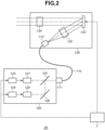
- Fig. 2 illustrates a configuration example of the light source unit 20.
- the light source unit 20 includes a first light source 121 that generates first light having a first wavelength band for generating the first modulated light, and a second light source 122 that generates second light having a second wavelength band for generating the second modulated light.
- the light source unit 20 further includes a digital mirror device (DMD) 133 as a spatial light modulator (modulator) that generates the first modulated light obtained by modulating the first light (incident light), and the second modulated light obtained by modulating the second light (incident light).
- DMD digital mirror device
- the light source unit 20 further includes a first optical system (mirrors 125 and 126, entrance portion 111, and optical system 132) that causes the first light from the first light source 121 and the second light from the second light source 122 to enter the DMD 133 functioning as a spatial light modulator.
- a first optical system mirrors 125 and 126, entrance portion 111, and optical system 132 that causes the first light from the first light source 121 and the second light from the second light source 122 to enter the DMD 133 functioning as a spatial light modulator.
- the light source unit 20 can include an illumination unit 120 and a modulation unit 130 connected by an optical fiber 110.
- the illumination unit 120 includes the first light source 121, the second light source 122, a first controller 123, a second controller 124, and the mirrors 125 and 126.
- the light path of the first light generated by the first light source 121, and the light path of the second light generated by the second light source 122 are combined by the mirrors 125 and 126, and the resultant light path is connected to the entrance portion 111 of the optical fiber 110.
- An exit portion 112 of the optical fiber 110 is connected to the modulation unit 130.
- the first controller 123 controls the first light source 121 in response to a command from the control unit 7.
- the control of the first light source 121 can include the control of turning on and off of the first light source 121.
- the control of the first light source 121 may also include the control of the intensity of the first light generated by the first light source 121.
- the first controller 123 includes a constant electric current circuit that supplies electric current having an electric current value conforming to a command value from the control unit 7, to the first light source 121.
- the first controller 123 includes a driving circuit that drives the first light source 121 based on a command value, and a photoelectric conversion sensor that partially receives the first light generated by the first light source 121, and is configured to feed back an output of the photoelectric conversion sensor to the driving circuit.
- the second controller 124 controls the second light source 122 in response to a command from the control unit 7.
- the control of the second light source 122 can include the control of turning on and off of the second light source 122.
- the control of the second light source 122 may also include the control of the intensity of the second light generated by the second light source 122.
- the second controller 124 includes a constant electric current circuit that supplies electric current having an electric current value conforming to a command value from the control unit 7, to the second light source 122.
- the second controller 124 includes a driving circuit that drives the second light source 122 based on a command value, and a photoelectric conversion sensor that partially receives the second light generated by the second light source 122, and is configured to feed back an output of the photoelectric conversion sensor to the driving circuit.
- the control unit 7 individually controls the first light source 121 and the second light source 122.
- the control unit 7 can control the first light source 121 and the second light source 122 so as to turn off one of the first light source 121 and the second light source 122 when turning on the other one of the first light source 121 and the second light source 122.
- a configuration in which, when one of the first light from the first light source 121 and the second light from the second light source 122 enters the spatial light modulator (the DMD 133), the other one of the first light and the second light does not enter the spatial light modulator can be employed. This can be implemented by a mechanism that selectively shuts off one of the controls of the first and second light sources 121 and 122 that are respectively performed by the first and second controllers 123 and 124 or one of the first light and the second light, for example.
- the curing light 9 is light for curing the imprint material IM, and can have an arbitrary wavelength band within a range of 300 nm to 380 nm as an example, but may have a wavelength band of 300 nm or less.
- the detection light 15 is light for detecting an alignment mark, and has a wavelength band of 550 nm to 750 nm as an example.
- the observation light 18 is light for observing a contact state of the imprint material IM and the mold M, and a filled state of the space between the substrate S and the mold M with the imprint material IM.
- a wavelength band that does not overlap wavelength bands of the curing light 9 and the detection light 15 can be selected from a wavelength band of 400 nm to 480 nm, for example.
- the modulated light 21 includes the first modulated light having a wavelength band that does not allow curing of the imprint material IM, and the second modulated light having a wavelength band that allows curing of the imprint material IM.
- a wavelength band of the modulated light 21 a wavelength band similar to that of the observation light 18 can be selected. For example, a wavelength band that does not overlap wavelength bands of the curing light 9 and the detection light 15 can be selected from a wavelength band of 400 nm to 480 nm.
- the first modulated light is generated by the modulation unit 130 (the DMD 133) modulating the first light generated by the first light source 121.
- the second modulated light is generated by the modulation unit 130 (the DMD 133) modulating the second light generated by the second light source 122. Wavelengths of the first light generated by the first light source 121 and the second light generated by the second light source 122 can be determined based on an upper limit of a wavelength band in which the imprint material IM cures.
- the wavelength of the first light generated by the first light source 121 can be set to about 460 nm, and the wavelength of the second light generated by the second light source 122 can be set to about 410 nm.
- the first light source 121 and the second light source 122 desirably generate single-wavelength light having a narrow wavelength width, and for example, a laser diode is suitable. Laser diodes are excellent in that turning on and off can be switched at high speed.
- the optical system 132 can include, for example, a light-collecting optical system and an illumination system (e.g., microlens array) that uniformizes light from the light-collecting optical system and illuminates the DMD 133.
- the DMD 133 includes a plurality of micromirrors (not illustrated) that each reflects light, and actuators that respectively drive the plurality of micromirrors.
- each of the actuators controls an angle of a corresponding micromirror to -12 degrees (ON state) or +12 degrees (OFF state) with respect to an array surface of the plurality of micromirrors.
- Light reflected by a micromirror in the ON state forms, as modulated light, an image on the substrate S via a projection optical system 134 (second optical system) that brings the DMD 133 and the substrate S into an optically-conjugate relationship.
- Light reflected by a micromirror in the OFF state is reflected in a direction in which the light does not reach the substrate S.
- a region projected on the substrate S when all the micromirrors are brought into the ON state is larger than the size of the maximum pattern formation region (shot region) of the substrate S.
- the maximum irradiated region can be set a region larger than the maximum pattern formation region by 1 mm or more.
- Another spatial light modulator such as a liquid crystal display (LCD) may be employed in place of the DMD 133.
- the optical systems included in the modulation unit 130 transmit both of the first light (first modulated light) having a wavelength that does not allow curing of the imprint material IM, and the second light (second modulated light) having a wavelength that allows curing of the imprint material IM.
- first modulated light having a wavelength that does not allow curing of the imprint material IM
- second modulated light having a wavelength that allows curing of the imprint material IM.
- the maximum light intensity of light that can be emitted onto a micromirror array decreases in a wavelength of 420 nm or less, and furthermore, in the vicinity of 400 nm being a boundary between ultraviolet light and visible light, the maximum light intensity of light that can be emitted onto a micromirror array drastically decreases to about 1/1000. It is therefore desirable to bring the wavelength of the first light source 121 and the wavelength of the second light source 122 closer to the vicinity of the upper limit of a wavelength band in which the imprint material IM cures, using a laser di
- the control unit 7 can generate control data for controlling the switching between the ON state and the OFF state of each micromirror of the DMD 133.
- the light intensity distribution data can include information regarding a time in which each micromirror is kept in the ON state, and information regarding a time in which each micromirror is kept in the OFF state, for example. As the number of micromirrors being in the ON state increases, and as the time of the ON state becomes longer, the pattern formation region of the substrate S can be exposed with a larger exposure amount.
- the control unit 7 includes a memory that stores light intensity distribution data for generating the first modulated light by modulating the first light, and light intensity distribution data for generating the second modulated light by modulating the second light.
- the light intensity distribution data for generating the first modulated light by modulating the first light includes light intensity distribution data for deforming the pattern formation region (shot region) of the substrate S into a target shape.
- the light intensity distribution data for generating the second modulated light by modulating the second light includes light intensity distribution data for curing (increasing the viscosity of) a portion of the imprint material IM on the substrate S, which corresponds to the peripheral portion (frame region) of the pattern formation region of the substrate S.
- a configuration in which the modulation unit 130 is shared by the first light source 121 and the second light source 122 is advantageous to downsize the modulation unit 130 or the light source unit 20, and thereby the structure of the imprint apparatus 1 can be simplified. This can make it easier to dispose the modulation unit 130 near the light path LP.
- a configuration in which the illumination unit 120 and the modulation unit 130 are separated from each other is advantageous to dispose the illumination unit 120 functioning as a heat source, at a position distant from the light path LP of the imprint apparatus 1. Nevertheless, the illumination unit 120 and the modulation unit 130 may be disposed in proximity to each other without using the optical fiber 110. Alternatively, the illumination unit 120 may be incorporated into the modulation unit 130.
- first light source 121 and the modulation unit 130 may be connected by a first optical fiber
- second light source 122 and the modulation unit 130 may be connected by a second optical fiber.
- a light path of first light emitted from the first optical fiber and a light path of second light emitted from the second optical fiber can be coupled.
- Fig. 3A illustrates a first operation example of the light source unit 20 in imprint processing executed by the imprint apparatus 1.
- the "imprint processing" indicates the progress of imprint processing.
- the imprint processing includes a contact process of bringing the imprint material IM on the substrate S and the mold M into contact with each other, an alignment process of performing alignment of the substrate S and the mold M after the contact process, and a curing process of curing the imprint material IM after the alignment process.
- the contact process is a process of bringing the imprint material IM on the substrate S and (the pattern region PR of) the mold M into contact with each other using the driving mechanism DRV.
- the contact process is started upon the start of contact between the imprint material IM on the substrate S and the pattern region PR of the mold M deformed into a protruding shape, and is ended when the entire region of the pattern region PR is planarized, for example.
- the imprint processing includes, as a process accompanied by the contact process, a driving process of bringing the imprint material IM on the substrate S and the mold M closer to each other using the driving mechanism DRV, and the process is described as "driving" in Fig. 3A .
- the alignment process based on a result detected by the detector 12, at least one of the substrate S and the mold M is driven by the driving mechanism DRV so that the pattern formation region of the substrate S and the pattern region PR of the mold M are aligned.
- the mold M can be deformed by the mold driving mechanism so that the pattern formation region (shot region) of the substrate S and the pattern region PR of the mold M are aligned.
- an undermentioned deformation process can be executed so that the pattern formation region of the substrate S and the pattern region PR of the mold M are aligned.
- a filling process is executed.
- a recessed portion included in the pattern in the pattern region PR is filled with the imprint material IM existing between the substrate S and the pattern region PR of the mold M, and an airspace existing between the substrate S and the pattern region PR of the mold M disappears.
- the alignment process and the filling process are described as "filling and alignment” in Fig. 3A .
- the filling process can be started prior to the alignment process.
- a curing process is described as "curing” and a separation process is described as "separation”.
- optical modulation performed by DMD indicates optical modulation performed by the DMD 133 of the light source unit 20.
- a partial curing process C indicates that the second modulated light generated by modulating the second light having a wavelength band that allows curing of (increases the viscosity of) the imprint material IM is emitted to the light path LP.
- the imprint material IM in the above-described frame region is cured (frame exposure is performed).
- a deformation process D described as "D" in fig.
- the first modulated light generated by modulating the first light having a wavelength band that does not allow curing of the imprint material IM is emitted to the light path LP.
- the pattern formation region of the substrate S is deformed to perform the alignment of the pattern formation region of the substrate S and the pattern region PR of the mold M.
- a period “OFF" in Fig. 3A indicates that neither the first modulated light nor the second modulated light is emitted to the light path LP.
- the DMD 133 is controlled and a light intensity distribution is switched from a light intensity distribution of the first modulated light to a light intensity distribution of the second modulated light.
- a period (timing, time length) of the partial curing process C in which frame exposure is performed can be determined so as to prevent the imprint material IM from being pushed out to the outside of the pattern formation region of the substrate S, by curing the imprint material IM in the frame region.
- a period (timing, time length) of the deformation process D can be determined so that the shape of the pattern formation region of the substrate S becomes a target shape at a time point at which the imprint material IM is cured by the curing light 9 from the curing light source 2 in the curing process. It is desirable that the substrate S is deformed at least during the alignment period, and the deformation process D is completed before the start of the curing process.
- the execution order of the processes is, however, not limited thereto.
- the processes may be executed in an opposite order or repeatedly executed a plurality of times.
- Fig. 3B illustrates a second operation example of the light source unit 20 in imprint processing executed by the imprint apparatus 1.
- a description method conforms to the description method in Fig. 3A .
- the period "OFF" in the example illustrated in Fig. 3A is omitted or shortened.
- the period of the partial curing process C and the period of the deformation process D cannot be overlapped.
- the partial curing process C is not executed in the contact process. This is because, if the imprint material IM is cured in the contact process even partially, the imprint material IM is prevented from spreading, and the filling in the subsequent filling process is disturbed.
- a time required for the alignment process and the filling process that progress concurrently with each other cannot be made shorter than a total time of the period of the partial curing process C and the period of the deformation process D.
- frame exposure is executed as described above.
- the execution period of the frame exposure is determined so as to prevent the imprint material IM from being pushed out to the outside of the pattern formation region of the substrate S (pattern region PR of the mold M).
- vibration control exposure is executed as described above.
- the execution time of the vibration control exposure is determined so as to reduce relative vibration between the substrate S and the mold M and enhance a convergence property of the alignment.
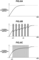
- Fig. 6A illustrates an example of a temporal change in deformation amount (thermal deformation amount) of (the pattern formation region of) the substrate S in the deformation process D in the first and second operation examples respectively illustrated in Figs. 3A and 3B .
- a change in deformation amount can be represented by a function including an exponential function, for example. By preliminarily obtaining a time constant of the exponential function, it is possible to determine the time of each deformation process D and a start timing of the deformation process D. In addition, the intensity of the first light may be adjusted.
- the common modulation unit 130 (the DMD 133) for light sources having different wavelengths, it is possible to provide a plurality of functions in an imprint apparatus without complicating the structure of the apparatus.
- Figs. 4A, 4B and 4C respectively illustrate third, fourth, and fifth operation examples of the imprint apparatus.
- the description method confirms to the description method in Fig. 3A .
- the third, fourth, and fifth operation examples can include at least a first operation O1, a second operation 02, and a third operation 03.
- the first operation O1 the first modulated light that does not cure the imprint material IM is supplied to the light path LP (i.e., the deformation process D is executed).
- the second operation O2 is executed after the first operation O1, and in the second operation 02, the second modulated light that cures the imprint material IM is supplied to the light path LP (i.e., the partial curing process C is executed).
- the third operation O3 is executed after the second operation O2, and in the third operation O3, the first modulated light that does not cure the imprint material IM is supplied to the light path LP (i.e., the deformation process D is executed).
- the second operation O2 and the third operation O3 can be executed concurrently with the alignment process.
- the second operation O2 can be started after the start of the alignment process.
- the first operation O1 is started before the start of the alignment process.
- the first operation O1 is started in the contact process (more specifically, at an arbitrary timing in the contact process).
- the first operation O1 can be started after the start of the alignment process.
- the third operation O3 can be executed so that the deformation of (the pattern formation region of) the substrate S for the alignment of the substrate S and the mold M is completed at the start of the curing process.
- the first operation O1 and the third operation O3 can be executed so that the deformation of (the pattern formation region of) the substrate S for the alignment of the substrate S and the mold M is completed at the start of the curing process.
- the deformation process D and the partial curing process C that can be only exclusively executed and have constraints on the respective execution times appear to be concurrently executed.
- a unit operation UO can be executed at least once between the second operation O2 and the third operation O3.
- the unit operation UO includes an operation in which the first modulated light is supplied to the light path LP (deformation process D) and an operation in which the second modulated light is supplied to the light path LP (partial curing process C).
- the deformation process D serving as the first operation O1, the deformation process D serving as the third operation O3, and the deformation process D in the unit operation UO can be executed so that the deformation of (the pattern formation region of) the substrate S for the alignment of the substrate S and the mold M is completed at the start of the curing process.
- the partial curing process C can include the frame exposure and/or vibration control exposure as above described.
- the execution period of the frame exposure is determined so as to prevent the imprint material IM from being pushed out to the outside of the pattern formation region of the substrate S.
- the vibration control exposure is executed so as to reduce relative vibration between the substrate S and the mold M and enhance a convergence property of alignment. In a case where both of the frame exposure and the vibration control exposure are executed, typically, the frame exposure is executed prior to the vibration control exposure.
- the temperature of the substrate S can decrease (i.e., the substrate S can release heat) after the end of the first operation O1.
- the temperature decrease needs to be compensated for.
- the execution timing of the second operation O2 frame exposure and/or vibration control exposure
- the first operation O1 can be started before the start of the alignment process.
- the partial curing process C and the deformation process D are normally started after the start of the alignment process and the filling process. This can impose restrictions on the shortening of the alignment process and the filling process. In other words, the execution time of the alignment process and the filling process cannot be made shorter than a time required for both of the partial curing process C and the deformation process D.
- the execution time of the alignment process and the filling process may be shorter than a required time from the start of the first operation O1 to the end of the third operation O3. This enables the deformation process D and the partial curing process C to be executed under the time constraints imposed on the processes, while shortening the execution time of the alignment process and the filling process as much as possible.
- the unit operation UO including the deformation process D and the partial curing process C is executed at least once or a plurality of times between the second operation O2 and the third operation O3.
- a time ratio between the deformation process D and the partial curing process C included in the unit operation UO can be arbitrarily set. In a case where the unit operation UO is executed a plurality of times, the ratio may be individually set for each of the unit operations UO.
- the time of each partial curing process C is shortened. This is advantageous to reduce heat release of the substrate S in each partial curing process C.
- the time of each partial curing process C may be determined such that the deformation of the substrate S caused by heat release of the substrate S within the time can be regarded as deformation in a linear shape. This is advantageous to more easily determine a heat input amount of the substrate S (emission amount of first modulated light) in each deformation process D.
- the unit operation UO is not inserted between the second operation O2 and the third operation O3.
- the time of the second operation O2 can be increased, and a temperature decrease of the substrate S in the time can be large.
- the number of times of switching between the deformation process D and the partial curing process C is small. This is advantageous to reduce a time required for switching, and/or to simplify a control parameter (control information) for controlling operations.
- the first operation O1 is started in the contact process, but the first operation O1 may be started after the start of the alignment process. Also in this case, the deformation process D and the partial curing process C that can be only exclusively executed and have constraints on the respective execution times appear to be concurrently executed.
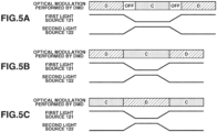
- Fig. 5A illustrates an example of the control of optical modulation performed by the DMD 133, and turning on and off of the first light source 121 and the second light source 122. Because the turning on and off of the first light source 121 and the second light source 122 have transient response characteristics, it is difficult to control the turning on and off of the first light source 121 and the second light source 122 completely exclusively. In other words, the first light source 121 and the second light source 122 can enter an intermediate state between the on state and the off state. In a case where the first light source 121 and the second light source 122 are in a transient state, both of the first light from the first light source 121 and the second light from the second light source 122 can enter the DMD 133.
- both of light obtained by modulating the first light and light obtained by modulating the second light can be emitted to the light path LP. This can cause undesirable deformation of the substrate S due to light obtained by disorderly modulating the second light by the DMD 133.
- the DMD 133 is controlled to be in the OFF state in which light from the DMD 133 is not emitted to the light path LP.
- it takes about 100 microseconds for switching between the turning on and off of the first light source 121 and the second light source 122, and it takes about 10 microseconds for switching between patterns of the DMD 133 (switching between modulation states), for example.
- Fig. 5B illustrates another example of the control of optical modulation performed by the DMD 133, and turning on and off of the first light source 121 and the second light source 122.
- an intentional OFF period when the DMD 133 is in the OFF state is omitted or shortened.
- Such control is advantageous to enhance throughput.
- an amount of deformation of the substrate S that is caused by the first light that does not cure the imprint material IM (light for the deformation process D) in a transient time is sometimes ignorable.
- the DMD 133 after the DMD 133 is changed from a modulation state for the deformation process D to a modulation state for the partial curing process C, the first light source 121 that generates the first light can be changed from the on state to the off state, and the second light source 122 that generates the second light can be changed from the off state to the on state.
- the DMD 133 can be changed from the modulation state for the partial curing process C to the modulation state for the deformation process D.
- Fig. 5C illustrates yet another example of the control of optical modulation performed by the DMD 133, and turning on and off of the first light source 121 and the second light source 122.
- an intentional OFF period when the DMD 133 is in the OFF state is omitted or shortened.
- Such control is advantageous to enhance throughput.
- an amount of deformation of the substrate S that is caused by the second light that cures the imprint material IM (light for the partial curing process C) in a transient time is sometimes ignorable.
- the DMD 133 after the DMD 133 is changed from a modulation state for the partial curing process C to a modulation state for the deformation process D, the first light source 121 that generates the first light can be changed from the off state to the on state, and the second light source 122 that generates the second light can be changed from the on state to the off state.
- the DMD 133 can be changed from the modulation state for the deformation process D to the modulation state for the partial curing process C.
- Fig. 6B illustrates an example of a temporal change in deformation amount (thermal deformation amount) of (the pattern formation region of) the substrate S that is caused in a case where the first, second, and third operations accompanied by a plurality of unit operations UO are executed in accordance with the third and fourth operation examples respectively illustrated in Figs. 4B and 4C .
- a white portion (ON) indicates the deformation process D
- a gray portion (OFF) indicates the partial curing process C.
- the partial curing process C (OFF) because the first modulated light is not emitted onto the substrate S, an amount of deformation caused by thermal expansion decreases.
- the subsequent deformation process D (ON) is, thus, to be controlled considering an amount for compensating for the decrease in deformation amount.
- a change in deformation amount can be represented by a function including an exponential function, for example.
- By preliminarily obtaining a time constant of the exponential function it is possible to determine the time of each deformation process D and a time ratio between the deformation process D and the partial curing process C.
- the intensity of the first light may be adjusted.
- the example illustrated in Fig. 6B and the example illustrated in Fig. 6C indicate a difference in change in thermal deformation amount that is obtained in a case where an execution time of each unit operation UO including the deformation process D and the partial curing process C (as a result, the number of times of the repeated unit operations UO) is varied.
- the example illustrated in Fig. 6B is advantageous to enhance throughput in that the number of times of switching between the deformation process D and the partial curing process C is small.
- the amount of thermal deformation can be controlled regarding a change in thermal deformation amount in each unit operation UO as a change in a linear shape.
- an increase/decrease width of a thermal deformation amount can be reduced, and the deformation of the pattern formation region of the substrate S can be precisely controlled.
- Second modulated light according to the third exemplary embodiment can be light modulated so as to increase the viscosity of the imprint material IM at an arbitrary point of the pattern formation region of the substrate S, and thereby strengthen bonding force exerted between the substrate S and the mold M by the imprint material IM.
- the emission of such second modulated light that can be referred to as a vibration control exposure is executed in the alignment process, and can enhance alignment accuracy.
- the substrate S and the mold M can individually vibrate by disturbance (i.e., relative vibration between the substrate S and the mold M is large).
- a control unit 7 includes a memory that stores light intensity distribution data for generating the first modulated light by modulating the first light, and light intensity distribution data for generating the second modulated light by modulating the second light.
- the light intensity distribution data for generating the second modulated light by modulating the second light includes light intensity distribution data for increasing the viscosity of the imprint material IM at an arbitrary point of the pattern formation region of the substrate S and strengthening bonding force exerted between the substrate S and the mold M via the imprint material IM.
- the viscosity of the imprint material IM at an arbitrary point of the pattern formation region of the substrate S is increased (vibration control exposure is executed).
- a period (timing, time length) of the partial curing process C in which the vibration control exposure is performed can be determined so as to reduce relative vibration between the substrate S and the mold M by partially increasing the viscosity of the imprint material IM and strengthening bonding force exerted between the substrate S and the mold M.
- the common modulation unit 130 (the DMD 133) for light sources having different wavelengths, it is possible to provide a mechanism of deforming the substrate and a mechanism of increasing the viscosity of the imprint material (vibration control exposure mechanism), without complicating the structure of the apparatus.
- First modulated light according to the fourth exemplary embodiment can be light modulated so as to increase the viscosity of the imprint material IM at an arbitrary point of the pattern formation region of the substrate S, and thereby strengthening bonding force exerted between the substrate S and the mold M by the imprint material IM.
- the emission of such first modulated light that can be referred to as a vibration control exposure is executed in the alignment process, and can enhance alignment accuracy.
- the substrate S and the mold M can individually vibrate by disturbance (i.e., relative vibration between the substrate S and the mold M is large).
- a control unit 7 includes a memory that stores light intensity distribution data for generating the first modulated light by modulating the first light, and light intensity distribution data for generating the second modulated light by modulating the second light.
- the light intensity distribution data for generating the first modulated light by modulating the first light includes can include light intensity distribution data for increasing the viscosity of the imprint material IM at an arbitrary point of the pattern formation region of the substrate S and strengthening bonding force exerted between the substrate S and the mold M via the imprint material IM.
- a period (timing, time length) of a vibration control exposure process in which the vibration control exposure is performed can be determined so as to reduce relative vibration between the substrate S and the mold M by partially increasing the viscosity of the imprint material IM and strengthening bonding force exerted between the substrate S and the mold M.
- the common modulation unit 130 (the DMD 133) for light sources with different distributions of irradiated regions on the substrate, it is possible to provide a mechanism of increasing the viscosity of the imprint material in the peripheral portion of the shot region (frame exposure), without complicating the structure of the apparatus.
- a light source unit 20 according to the fifth exemplary embodiment may be provided with a mechanism of emitting third modulated light onto the substrate in addition to the first modulated light and the second modulated light.
- the light source unit 20 illustrated in Fig. 2 can include a third light source that emits third light having a third wavelength band.
- the third light source can be controlled by a third controller.
- the first modulated light can be light having a light intensity distribution for deforming the shot region into a target shape
- the second modulated light can be light for increasing the viscosity of the imprint material in the peripheral portion of the shot region
- the third modulated light can be light for enhancing a convergence property of alignment.
- the common modulation unit 130 (the DMD 133) for light sources having different wavelengths, it is possible to provide a mechanism of deforming the substrate and a mechanism of increasing the viscosity of the imprint material (vibration control exposure mechanism), without complicating the structure of the apparatus.
- the common modulation unit 130 can also be used for light sources with different distributions of irradiated regions on the substrate.
- the light source unit 20 can further include another light source.
- the pattern of cured material formed using the imprint apparatus is permanently used in at least part of various products, or temporarily used in manufacturing various products.
- a product is, for example, an electrical circuit element, an optical element, a microelectromechanical system (MEMS), a recording element, a sensor, or a mold.
- the electrical circuit element include a volatile or nonvolatile semiconductor memory such as a dynamic random access memory (DRAM), a static RAM (SRAM), a flash memory, or a magnetic RAM (MRAM), and a semiconductor element such as a large-scale integrated circuit (LSI), a charge-coupled device (CCD) sensor, an image sensor, or an FPGA.
- DRAM dynamic random access memory
- SRAM static RAM
- MRAM magnetic RAM
- LSI large-scale integrated circuit
- CCD charge-coupled device
- Examples of the optical element include a microlens, a light guide member, a waveguide, an antireflection film, a diffraction grating, a polarization element, a color filter, a light-emitting element, a display, and a solar battery.
- Examples of the MEMS include a DMD, a micro flow path, and an electromechanical transduction element.
- Examples of the recording element include an optical disc such as a compact disc (CD) or a digital versatile disc (DVD), a magnetic disc, a magneto-optic disc, and a magnetic head.
- Examples of the sensor include a magnetic sensor, an optical sensor, and a gyro sensor.
- Examples of the mold include an imprinting mold.
- the pattern of the cured material is directly used as a component of at least part of the above-described products, or temporarily used as a resist mask. After etching or ion implantation is performed in a processing process of the substrate, the resist mask is removed.
- a product manufacturing method of forming a pattern on a substrate using an imprint apparatus, processing the substrate on which the pattern is formed, and manufacturing a product from the processed substrate will be described.
- a substrate 1z such as a silicon wafer, that has a surface on which processed material 2z, such as insulating material, is formed is prepared, and subsequently, imprint material 3z is applied onto the surface of the processed material 2z by an inkjet method or the like.
- Fig. 7A illustrates a state in which the imprint material 3z shaped into a plurality of droplets is applied on the substrate 1z.
- an imprinting mold 4z is caused to face the imprint material 3z on the substrate 1z such that a side on which an uneven pattern is formed faces the imprint material 3z.
- the substrate 1z on which the imprint material 3z is applied and the mold 4z are brought into contact with each other, and pressure is added.
- a clearance gap between the mold 4z and the processed material 2z is filled with the imprint material 3z. If light is emitted in this state via the mold 4z as curing energy, the imprint material 3z is cured.
- a pattern of cured material of the imprint material 3z is formed on the substrate 1z.
- the pattern of the cured material has a shape in which a recessed portion of the mold corresponds to a protruding portion of the cured material and a protruding portion of the mold corresponds to a recessed portion of the cured material.
- the uneven pattern of the mold 4z is transferred onto the imprint material 3z.
- etching is performed using the pattern of the cured material as an etching resistance mask, a portion having no cured material or having a thin remaining cured material in the surface of the processed material 2z is removed, and then grooves 5z are formed.
- Fig. 7F if the pattern of the cured material is removed, a product in which the grooves 5z are formed on the surface of the processed material 2z can be obtained.
- the pattern of the cured material is removed in this example, the pattern of the cured material may not be removed and used, for example, as an interlayer insulation film included in a semiconductor element, i.e., as a component of the product.
- a substrate 1y made of material such as quartz glass is prepared, and subsequently, imprint material 3y is applied onto the surface of the substrate 1y by the inkjet method or the like.
- a layer made of another material such as metal or a metal compound may be provided on the surface of the substrate 1y as necessary.
- an imprinting mold 4y is caused to face the imprint material 3y on the substrate 1y such that a side on which an uneven pattern is formed faces the imprint material 3y.
- the substrate 1y on which the imprint material 3y is applied and the mold 4y are brought into contact with each other, and pressure is added. A clearance gap between the mold 4y and the substrate 1y is filled with the imprint material 3y. If light is emitted in this state via the mold 4y, the imprint material 3y is cured.
- a pattern of a cured material of the imprint material 3y is formed on the substrate 1y.
- a product including the pattern of the cured material as a component is obtained.
- the substrate 1y is etched in the state illustrated in Fig. 8D using the pattern of the cured material as a mask, a product in which a recessed portion and a protruding portion are inversely provided with respect to the mold 4y, such as an imprinting mold, can be also be obtained.
Landscapes
- Physics & Mathematics (AREA)
- General Physics & Mathematics (AREA)
- Exposure Of Semiconductors, Excluding Electron Or Ion Beam Exposure (AREA)
- Shaping Of Tube Ends By Bending Or Straightening (AREA)
- Telephone Function (AREA)
- Confectionery (AREA)
Claims (20)
- Appareil d'empreinte (1) configuré pour exécuter un traitement d'empreinte comprenantun processus de contact consistant à mettre en contact l'un avec l'autre un matériau d'empreinte (IM) sur un substrat (S) et un moule (M),un processus d'alignement consistant à effectuer un alignement du substrat et du moule après le processus de contact, etun processus de durcissement consistant à durcir le matériau d'empreinte après le processus d'alignement, le matériau d'empreinte étant dans un état dans lequel le matériau d'empreinte et le moule sont en contact l'un avec l'autre, l'appareil d'empreinte (1) comprenant :un modulateur (133) configuré pour moduler une lumière incidente ;un premier système optique (125, 126, 111, 112, 132) configuré pour guider une première lumière d'une première source lumineuse (121) vers le modulateur (133), et une deuxième lumière d'une deuxième source lumineuse (122) vers le modulateur (133), la deuxième lumière ayant une longueur d'onde différente d'une longueur d'onde de la première lumière ; etun deuxième système optique (134, 22) configuré pour guider une lumière modulée (21) ayant été modulée par le modulateur (133) vers le substrat (S),dans lequel, du fait du guidage vers le substrat (S) de la première lumière modulée obtenue par le modulateur (133) modulant la première lumière, le substrat (S) est déformé pour l'alignement du substrat (S) et du moule (M),dans lequel, du fait du guidage vers le substrat (S) de la deuxième lumière modulée qui durcit partiellement le matériau d'empreinte et qui est générée par le modulateur (133) modulant la deuxième lumière, la viscosité du matériau d'empreinte (IM) fourni sur le substrat (S) est augmentée, etdans lequel l'appareil d'empreinte est configuré pour effectuer une opération (D) de guidage de la première lumière modulée et une opération (C) de guidage de la deuxième lumière modulée à des moments différents l'un de l'autre, et pour effectuer l'opération (C) de guidage de la deuxième lumière modulée au cours d'un processus d'alignement consistant à effectuer un alignement du substrat (S) et du moule (M), après que le matériau d'empreinte (IM) sur le substrat (S) et le moule (M) ont été mis en contact l'un avec l'autre.
- Appareil d'empreinte selon la revendication 1, comprenant en outre un élément optique (126) configuré pour guider la deuxième lumière de la deuxième source lumineuse vers le modulateur sur un trajet de lumière entre la première source lumineuse et le modulateur.
- Appareil d'empreinte selon la revendication 2, dans lequel l'élément optique est un miroir.
- Appareil d'empreinte selon la revendication 1, dans lequel l'intensité de la première lumière et l'intensité de la deuxième lumière sont différentes l'une de l'autre.
- Appareil d'empreinte selon la revendication 1, dans lequel le premier système optique comprend une fibre optique (110) configurée pour guider la première lumière de la première source lumineuse vers le modulateur.
- Appareil d'empreinte selon la revendication 1, dans lequel le modulateur comprend un dispositif à miroir numérique.
- Appareil d'empreinte selon la revendication 1, comprenant en outre :une source lumineuse de durcissement (2) configurée pour émettre une lumière (9) destinée à durcir le matériau d'empreinte ; etun miroir dichroïque (24) configuré pour transmettre la lumière (21) modulée par le modulateur et réfléchir la lumière (9) provenant de la source lumineuse de durcissement.
- Appareil d'empreinte selon la revendication 1, dans lequel, lors de l'exécution de l'opération (D) de guidage de la première lumière modulée et de l'opération (C) de guidage de la deuxième lumière modulée à des moments différents l'un de l'autre, l'appareil d'empreinte est configuré pour effectuerune première opération (01) lors de laquelle la première lumière modulée est fournie à un trajet de lumière (LP) vers le substrat (S) à travers le moule (M) et le matériau d'empreinte (IM), une deuxième opération (O2) lors de laquelle la deuxième lumière modulée est fournie au trajet de lumière (LP) après la première opération (01), et une troisième opération (O3) lors de laquelle la première lumière modulée est fournie au trajet de lumière (LP) après la deuxième opération (O2), etdans lequel la deuxième opération (O2) et la troisième opération (O3) sont exécutées en même temps que le processus d'alignement.
- Appareil d'empreinte selon la revendication 8, configuré de façon que la première opération soit lancée avant le début du processus d'alignement.
- Appareil d'empreinte selon la revendication 8, configuré de façon que la première opération soit lancée lors du processus de contact.
- Appareil d'empreinte selon la revendication 8, configuré de façon que la troisième opération soit exécutée de telle sorte que la déformation du substrat aux fins de l'alignement du substrat et du moule soit achevée lors d'un début du processus de durcissement.
- Appareil d'empreinte selon la revendication 8, configuré de façon qu'une opération unitaire (UO) comprenant une opération lors de laquelle la première lumière modulée est fournie au trajet de lumière et une opération lors de laquelle la deuxième lumière modulée est fournie au trajet de lumière soit exécutée au moins une fois entre la deuxième opération et la troisième opération.
- Appareil d'empreinte selon la revendication 8, dans lequel la première source lumineuse et la deuxième source lumineuse sont commandées de telle sorte que lorsque l'une de la première source lumineuse et de la deuxième source lumineuse est activée, l'autre de la première source lumineuse et de la deuxième source lumineuse soit désactivée.
- Appareil d'empreinte selon la revendication 8, configuré de façon que lorsque l'une ou l'autre de la première lumière et de la deuxième lumière pénètre dans le modulateur, l'autre de la première lumière et de la deuxième lumière ne pénètre pas dans le modulateur.
- Appareil d'empreinte selon la revendication 8, dans lequel une bande de longueur d'onde de la première lumière et une bande de longueur d'onde de la deuxième lumière ne se chevauchent pas.
- Appareil d'empreinte selon la revendication 8, configuré de telle sorte que lors de la deuxième opération, le modulateur fournit au trajet de lumière, en tant que deuxième lumière modulée, une lumière modulée ayant une distribution d'intensité lumineuse qui permet de durcir une partie du matériau d'empreinte dans une partie périphérique d'une région de formation de motif du substrat.
- Appareil d'empreinte selon la revendication 8, configuré de façon que lors du processus de durcissement, la lumière (9) qui durcit le matériau d'empreinte soit fournie au trajet de lumière.
- Appareil d'empreinte selon la revendication 1, dans lequel
l'appareil d'empreinte est configuré pour effectuer une opération (OFF) entre l'opération (C) de guidage de la deuxième lumière modulée et l'opération (D) de guidage de la première lumière modulée, au cours de laquelle la première lumière et la deuxième lumière ne sont ni l'une ni l'autre incidentes sur le modulateur et le modulateur est commandé de telle sorte qu'une distribution d'intensité lumineuse soit amenée à passer d'une distribution d'intensité lumineuse de la première lumière modulée à une distribution d'intensité lumineuse de la deuxième lumière modulée. - Appareil d'empreinte selon la revendication 1, dans lequel l'une de la première lumière et de la deuxième lumière est sélectivement incidente sur le modulateur.
- Procédé de fabrication de produit comprenant :la formation d'un motif sur un substrat par l'appareil d'empreinte selon l'une quelconque des revendications 1 à 19 ; etle traitement du substrat sur lequel le motif est formé,dans lequel le produit est fabriqué à partir du substrat.
Priority Applications (1)
| Application Number | Priority Date | Filing Date | Title |
|---|---|---|---|
| EP24170999.7A EP4398040A3 (fr) | 2018-11-08 | 2019-10-29 | Appareil d'impression et procédé de fabrication de produit |
Applications Claiming Priority (2)
| Application Number | Priority Date | Filing Date | Title |
|---|---|---|---|
| JP2018210925A JP7202148B2 (ja) | 2018-11-08 | 2018-11-08 | インプリント装置および物品製造方法 |
| JP2018210917A JP7289633B2 (ja) | 2018-11-08 | 2018-11-08 | インプリント装置および物品製造方法 |
Related Child Applications (2)
| Application Number | Title | Priority Date | Filing Date |
|---|---|---|---|
| EP24170999.7A Division-Into EP4398040A3 (fr) | 2018-11-08 | 2019-10-29 | Appareil d'impression et procédé de fabrication de produit |
| EP24170999.7A Division EP4398040A3 (fr) | 2018-11-08 | 2019-10-29 | Appareil d'impression et procédé de fabrication de produit |
Publications (3)
| Publication Number | Publication Date |
|---|---|
| EP3650937A1 EP3650937A1 (fr) | 2020-05-13 |
| EP3650937C0 EP3650937C0 (fr) | 2024-05-22 |
| EP3650937B1 true EP3650937B1 (fr) | 2024-05-22 |
Family
ID=68392746
Family Applications (2)
| Application Number | Title | Priority Date | Filing Date |
|---|---|---|---|
| EP19205896.4A Active EP3650937B1 (fr) | 2018-11-08 | 2019-10-29 | Appareil d'impression et procédé de fabrication d'un produit |
| EP24170999.7A Pending EP4398040A3 (fr) | 2018-11-08 | 2019-10-29 | Appareil d'impression et procédé de fabrication de produit |
Family Applications After (1)
| Application Number | Title | Priority Date | Filing Date |
|---|---|---|---|
| EP24170999.7A Pending EP4398040A3 (fr) | 2018-11-08 | 2019-10-29 | Appareil d'impression et procédé de fabrication de produit |
Country Status (5)
| Country | Link |
|---|---|
| US (4) | US11226554B2 (fr) |
| EP (2) | EP3650937B1 (fr) |
| KR (3) | KR102641226B1 (fr) |
| CN (1) | CN111158212B (fr) |
| TW (1) | TWI771623B (fr) |
Families Citing this family (4)
| Publication number | Priority date | Publication date | Assignee | Title |
|---|---|---|---|---|
| US20240014052A1 (en) * | 2020-08-13 | 2024-01-11 | Ci Systems (Israel) Ltd. | Synchronization between temperature measurement device and radiation sources |
| KR102586152B1 (ko) * | 2020-11-04 | 2023-10-06 | 한국기계연구원 | 편광 필터의 제조 장치 및 방법 |
| JP7804454B2 (ja) * | 2021-12-20 | 2026-01-22 | キヤノン株式会社 | インプリント方法、インプリント装置および物品製造方法 |
| JP7716343B2 (ja) * | 2022-01-06 | 2025-07-31 | キヤノン株式会社 | インプリント装置、インプリント方法、および物品製造方法 |
Citations (1)
| Publication number | Priority date | Publication date | Assignee | Title |
|---|---|---|---|---|
| US20180301331A1 (en) * | 2017-04-17 | 2018-10-18 | Canon Kabushiki Kaisha | Imprint apparatus and method of manufacturing article |
Family Cites Families (36)
| Publication number | Priority date | Publication date | Assignee | Title |
|---|---|---|---|---|
| KR100968687B1 (ko) * | 2005-08-03 | 2010-07-06 | 페톤 가부시끼가이샤 | 반도체 장치의 제조 방법 및 반도체 장치의 제조 장치 |
| US20090128451A1 (en) | 2005-08-25 | 2009-05-21 | Kei Tokui | Image display device |
| US20090022712A1 (en) | 2006-01-24 | 2009-01-22 | University Of Virginia Patent Foundation | Compositions and Methods for Inhibiting Leukocyte Function |
| WO2008099795A2 (fr) * | 2007-02-06 | 2008-08-21 | Canon Kabushiki Kaisha | Procédé et appareil d'empreinte |
| JP5105984B2 (ja) * | 2007-07-26 | 2012-12-26 | 住友重機械工業株式会社 | ビーム照射装置、及び、レーザアニール方法 |
| JP2013069918A (ja) | 2011-09-22 | 2013-04-18 | Toshiba Corp | インプリント方法およびインプリント装置 |
| JP5535164B2 (ja) * | 2011-09-22 | 2014-07-02 | 株式会社東芝 | インプリント方法およびインプリント装置 |
| JP5686779B2 (ja) | 2011-10-14 | 2015-03-18 | キヤノン株式会社 | インプリント装置、それを用いた物品の製造方法 |
| JP6552410B2 (ja) * | 2012-05-30 | 2019-07-31 | ロリク アーゲーRolic Ag | 個別にパターン化された異方性を有する素子の高速な製造 |
| JP6294680B2 (ja) * | 2014-01-24 | 2018-03-14 | キヤノン株式会社 | インプリント装置、および物品の製造方法 |
| JP6480680B2 (ja) * | 2014-08-02 | 2019-03-13 | 株式会社アドテックエンジニアリング | 照度割合変更方法及び露光方法 |
| JP2016042498A (ja) * | 2014-08-13 | 2016-03-31 | キヤノン株式会社 | インプリント装置および物品製造方法 |
| JP6632270B2 (ja) * | 2014-09-08 | 2020-01-22 | キヤノン株式会社 | インプリント装置、インプリント方法および物品の製造方法 |
| US9429692B1 (en) * | 2015-02-09 | 2016-08-30 | Microsoft Technology Licensing, Llc | Optical components |
| JP6282298B2 (ja) | 2015-06-10 | 2018-02-21 | キヤノン株式会社 | インプリント装置、インプリント方法、および物品の製造方法 |
| US10386737B2 (en) * | 2015-06-10 | 2019-08-20 | Canon Kabushiki Kaisha | Imprint apparatus and method for producing article |
| JP2017118054A (ja) * | 2015-12-25 | 2017-06-29 | キヤノン株式会社 | インプリント装置、インプリント方法、および物品の製造方法 |
| JP6827785B2 (ja) * | 2016-11-30 | 2021-02-10 | キヤノン株式会社 | インプリント装置、インプリント方法、および物品の製造方法 |
| JP6824713B2 (ja) * | 2016-11-30 | 2021-02-03 | キヤノン株式会社 | インプリント方法、インプリント装置、型、および物品の製造方法 |
| JP6971567B2 (ja) * | 2016-12-16 | 2021-11-24 | キヤノン株式会社 | 位置合わせ装置、位置合わせ方法、リソグラフィ装置、および物品製造方法 |
| US11175598B2 (en) * | 2017-06-30 | 2021-11-16 | Canon Kabushiki Kaisha | Imprint apparatus and method of manufacturing article |
| JP7089348B2 (ja) * | 2017-07-28 | 2022-06-22 | キヤノン株式会社 | インプリント装置、インプリント方法および物品製造方法 |
| JP7039222B2 (ja) * | 2017-09-11 | 2022-03-22 | キオクシア株式会社 | インプリント装置及びインプリント方法 |
| JP7027099B2 (ja) * | 2017-09-29 | 2022-03-01 | キヤノン株式会社 | インプリント装置及び物品の製造方法 |
| JP7030533B2 (ja) * | 2018-01-15 | 2022-03-07 | キオクシア株式会社 | インプリント装置、インプリント方法、及び半導体装置の製造方法 |
| JP7241548B2 (ja) * | 2018-02-19 | 2023-03-17 | キヤノン株式会社 | インプリント装置、平坦化層形成装置、形成装置、制御方法、および、物品製造方法 |
| JP7210162B2 (ja) * | 2018-05-24 | 2023-01-23 | キヤノン株式会社 | インプリント装置、インプリント方法および物品の製造方法 |
| JP7204464B2 (ja) * | 2018-12-12 | 2023-01-16 | キヤノン株式会社 | インプリント方法、インプリント装置および物品製造方法 |
| JP7194010B2 (ja) * | 2018-12-20 | 2022-12-21 | キヤノン株式会社 | インプリント装置および物品製造方法 |
| JP7256684B2 (ja) * | 2019-05-14 | 2023-04-12 | キヤノン株式会社 | インプリント装置、インプリント方法および物品製造方法 |
| JP7358192B2 (ja) * | 2019-10-25 | 2023-10-10 | キヤノン株式会社 | インプリント装置、インプリント方法及び物品の製造方法 |
| JP7379091B2 (ja) * | 2019-10-30 | 2023-11-14 | キヤノン株式会社 | インプリント装置、インプリント方法、及び物品の製造方法 |
| JP7433861B2 (ja) * | 2019-11-27 | 2024-02-20 | キヤノン株式会社 | インプリント装置、インプリント方法、物品の製造方法、基板、および、型 |
| JP7403325B2 (ja) * | 2020-01-20 | 2023-12-22 | キヤノン株式会社 | インプリント方法、インプリント装置、および物品の製造方法 |
| JP7804454B2 (ja) * | 2021-12-20 | 2026-01-22 | キヤノン株式会社 | インプリント方法、インプリント装置および物品製造方法 |
| JP7716343B2 (ja) * | 2022-01-06 | 2025-07-31 | キヤノン株式会社 | インプリント装置、インプリント方法、および物品製造方法 |
-
2019
- 2019-10-29 EP EP19205896.4A patent/EP3650937B1/fr active Active
- 2019-10-29 EP EP24170999.7A patent/EP4398040A3/fr active Pending
- 2019-10-29 TW TW108138996A patent/TWI771623B/zh active
- 2019-11-04 US US16/673,804 patent/US11226554B2/en active Active
- 2019-11-06 CN CN201911076450.8A patent/CN111158212B/zh active Active
- 2019-11-07 KR KR1020190141428A patent/KR102641226B1/ko active Active
-
2021
- 2021-12-07 US US17/544,447 patent/US11921423B2/en active Active
-
2023
- 2023-12-20 US US18/390,910 patent/US12372866B2/en active Active
-
2024
- 2024-02-22 KR KR1020240025586A patent/KR102687480B1/ko active Active
- 2024-07-17 KR KR1020240094126A patent/KR102936994B1/ko active Active
-
2025
- 2025-06-30 US US19/255,673 patent/US20250328073A1/en active Pending
Patent Citations (1)
| Publication number | Priority date | Publication date | Assignee | Title |
|---|---|---|---|---|
| US20180301331A1 (en) * | 2017-04-17 | 2018-10-18 | Canon Kabushiki Kaisha | Imprint apparatus and method of manufacturing article |
Also Published As
| Publication number | Publication date |
|---|---|
| US20240126165A1 (en) | 2024-04-18 |
| US20220091502A1 (en) | 2022-03-24 |
| KR20240031272A (ko) | 2024-03-07 |
| KR102936994B1 (ko) | 2026-03-11 |
| KR102641226B1 (ko) | 2024-02-29 |
| KR20200053428A (ko) | 2020-05-18 |
| US11226554B2 (en) | 2022-01-18 |
| US20200150529A1 (en) | 2020-05-14 |
| US20250328073A1 (en) | 2025-10-23 |
| EP3650937C0 (fr) | 2024-05-22 |
| US12372866B2 (en) | 2025-07-29 |
| KR20240115792A (ko) | 2024-07-26 |
| TW202036667A (zh) | 2020-10-01 |
| CN111158212A (zh) | 2020-05-15 |
| EP3650937A1 (fr) | 2020-05-13 |
| TWI771623B (zh) | 2022-07-21 |
| KR102687480B1 (ko) | 2024-07-24 |
| US11921423B2 (en) | 2024-03-05 |
| CN111158212B (zh) | 2023-12-29 |
| EP4398040A3 (fr) | 2025-07-02 |
| EP4398040A2 (fr) | 2024-07-10 |
Similar Documents
| Publication | Publication Date | Title |
|---|---|---|
| US12372866B2 (en) | Imprint apparatus and product manufacturing method | |
| US11413793B2 (en) | Imprint apparatus, imprint method, and method for manufacturing product | |
| US9927700B2 (en) | Imprint apparatus, and method of manufacturing article | |
| US11442361B2 (en) | Imprint method, imprint apparatus, and method of manufacturing article | |
| JP7764542B2 (ja) | インプリント装置および物品製造方法 | |
| JP7202148B2 (ja) | インプリント装置および物品製造方法 | |
| US11833719B2 (en) | Imprint apparatus, imprint method, and method for manufacturing article | |
| US11480872B2 (en) | Imprint apparatus, imprint method, and method for manufacturing article | |
| US20240391160A1 (en) | Imprint apparatus and article manufacturing method | |
| US20260118785A1 (en) | Imprint method, imprint apparatus and article manufacturing method | |
| KR102831253B1 (ko) | 임프린트 장치 및 물품 제조 방법 | |
| KR20260062863A (ko) | 임프린트 방법, 임프린트 장치 및 물품 제조 방법 |
Legal Events
| Date | Code | Title | Description |
|---|---|---|---|
| PUAI | Public reference made under article 153(3) epc to a published international application that has entered the european phase |
Free format text: ORIGINAL CODE: 0009012 |
|
| STAA | Information on the status of an ep patent application or granted ep patent |
Free format text: STATUS: THE APPLICATION HAS BEEN PUBLISHED |
|
| AK | Designated contracting states |
Kind code of ref document: A1 Designated state(s): AL AT BE BG CH CY CZ DE DK EE ES FI FR GB GR HR HU IE IS IT LI LT LU LV MC MK MT NL NO PL PT RO RS SE SI SK SM TR |
|
| AX | Request for extension of the european patent |
Extension state: BA ME |
|
| STAA | Information on the status of an ep patent application or granted ep patent |
Free format text: STATUS: REQUEST FOR EXAMINATION WAS MADE |
|
| 17P | Request for examination filed |
Effective date: 20201113 |
|
| RBV | Designated contracting states (corrected) |
Designated state(s): AL AT BE BG CH CY CZ DE DK EE ES FI FR GB GR HR HU IE IS IT LI LT LU LV MC MK MT NL NO PL PT RO RS SE SI SK SM TR |
|
| STAA | Information on the status of an ep patent application or granted ep patent |
Free format text: STATUS: EXAMINATION IS IN PROGRESS |
|
| 17Q | First examination report despatched |
Effective date: 20221004 |
|
| GRAP | Despatch of communication of intention to grant a patent |
Free format text: ORIGINAL CODE: EPIDOSNIGR1 |
|
| STAA | Information on the status of an ep patent application or granted ep patent |
Free format text: STATUS: GRANT OF PATENT IS INTENDED |
|
| RIC1 | Information provided on ipc code assigned before grant |
Ipc: G03F 9/00 20060101ALI20231017BHEP Ipc: G03F 7/00 20060101AFI20231017BHEP |
|
| INTG | Intention to grant announced |
Effective date: 20231117 |
|
| GRAJ | Information related to disapproval of communication of intention to grant by the applicant or resumption of examination proceedings by the epo deleted |
Free format text: ORIGINAL CODE: EPIDOSDIGR1 |
|
| STAA | Information on the status of an ep patent application or granted ep patent |
Free format text: STATUS: EXAMINATION IS IN PROGRESS |
|
| GRAP | Despatch of communication of intention to grant a patent |
Free format text: ORIGINAL CODE: EPIDOSNIGR1 |
|
| STAA | Information on the status of an ep patent application or granted ep patent |
Free format text: STATUS: GRANT OF PATENT IS INTENDED |
|
| INTC | Intention to grant announced (deleted) | ||
| INTG | Intention to grant announced |
Effective date: 20240112 |
|
| GRAS | Grant fee paid |
Free format text: ORIGINAL CODE: EPIDOSNIGR3 |
|
| GRAA | (expected) grant |
Free format text: ORIGINAL CODE: 0009210 |
|
| STAA | Information on the status of an ep patent application or granted ep patent |
Free format text: STATUS: THE PATENT HAS BEEN GRANTED |
|
| AK | Designated contracting states |
Kind code of ref document: B1 Designated state(s): AL AT BE BG CH CY CZ DE DK EE ES FI FR GB GR HR HU IE IS IT LI LT LU LV MC MK MT NL NO PL PT RO RS SE SI SK SM TR |
|
| REG | Reference to a national code |
Ref country code: GB Ref legal event code: FG4D |
|
| REG | Reference to a national code |
Ref country code: CH Ref legal event code: EP |
|
| REG | Reference to a national code |
Ref country code: DE Ref legal event code: R096 Ref document number: 602019052525 Country of ref document: DE |
|
| REG | Reference to a national code |
Ref country code: IE Ref legal event code: FG4D |
|
| U01 | Request for unitary effect filed |
Effective date: 20240617 |
|
| U07 | Unitary effect registered |
Designated state(s): AT BE BG DE DK EE FI FR IT LT LU LV MT NL PT SE SI Effective date: 20240625 |
|
| PG25 | Lapsed in a contracting state [announced via postgrant information from national office to epo] |
Ref country code: IS Free format text: LAPSE BECAUSE OF FAILURE TO SUBMIT A TRANSLATION OF THE DESCRIPTION OR TO PAY THE FEE WITHIN THE PRESCRIBED TIME-LIMIT Effective date: 20240922 |
|
| PG25 | Lapsed in a contracting state [announced via postgrant information from national office to epo] |
Ref country code: HR Free format text: LAPSE BECAUSE OF FAILURE TO SUBMIT A TRANSLATION OF THE DESCRIPTION OR TO PAY THE FEE WITHIN THE PRESCRIBED TIME-LIMIT Effective date: 20240522 |
|
| PG25 | Lapsed in a contracting state [announced via postgrant information from national office to epo] |
Ref country code: GR Free format text: LAPSE BECAUSE OF FAILURE TO SUBMIT A TRANSLATION OF THE DESCRIPTION OR TO PAY THE FEE WITHIN THE PRESCRIBED TIME-LIMIT Effective date: 20240823 |
|
| PG25 | Lapsed in a contracting state [announced via postgrant information from national office to epo] |
Ref country code: ES Free format text: LAPSE BECAUSE OF FAILURE TO SUBMIT A TRANSLATION OF THE DESCRIPTION OR TO PAY THE FEE WITHIN THE PRESCRIBED TIME-LIMIT Effective date: 20240522 |
|
| U20 | Renewal fee for the european patent with unitary effect paid |
Year of fee payment: 6 Effective date: 20240919 |
|
| PG25 | Lapsed in a contracting state [announced via postgrant information from national office to epo] |
Ref country code: PL Free format text: LAPSE BECAUSE OF FAILURE TO SUBMIT A TRANSLATION OF THE DESCRIPTION OR TO PAY THE FEE WITHIN THE PRESCRIBED TIME-LIMIT Effective date: 20240522 |
|
| PG25 | Lapsed in a contracting state [announced via postgrant information from national office to epo] |
Ref country code: PL Free format text: LAPSE BECAUSE OF FAILURE TO SUBMIT A TRANSLATION OF THE DESCRIPTION OR TO PAY THE FEE WITHIN THE PRESCRIBED TIME-LIMIT Effective date: 20240522 Ref country code: NO Free format text: LAPSE BECAUSE OF FAILURE TO SUBMIT A TRANSLATION OF THE DESCRIPTION OR TO PAY THE FEE WITHIN THE PRESCRIBED TIME-LIMIT Effective date: 20240822 Ref country code: IS Free format text: LAPSE BECAUSE OF FAILURE TO SUBMIT A TRANSLATION OF THE DESCRIPTION OR TO PAY THE FEE WITHIN THE PRESCRIBED TIME-LIMIT Effective date: 20240922 Ref country code: HR Free format text: LAPSE BECAUSE OF FAILURE TO SUBMIT A TRANSLATION OF THE DESCRIPTION OR TO PAY THE FEE WITHIN THE PRESCRIBED TIME-LIMIT Effective date: 20240522 Ref country code: GR Free format text: LAPSE BECAUSE OF FAILURE TO SUBMIT A TRANSLATION OF THE DESCRIPTION OR TO PAY THE FEE WITHIN THE PRESCRIBED TIME-LIMIT Effective date: 20240823 Ref country code: ES Free format text: LAPSE BECAUSE OF FAILURE TO SUBMIT A TRANSLATION OF THE DESCRIPTION OR TO PAY THE FEE WITHIN THE PRESCRIBED TIME-LIMIT Effective date: 20240522 Ref country code: RS Free format text: LAPSE BECAUSE OF FAILURE TO SUBMIT A TRANSLATION OF THE DESCRIPTION OR TO PAY THE FEE WITHIN THE PRESCRIBED TIME-LIMIT Effective date: 20240822 |
|
| PG25 | Lapsed in a contracting state [announced via postgrant information from national office to epo] |
Ref country code: CZ Free format text: LAPSE BECAUSE OF FAILURE TO SUBMIT A TRANSLATION OF THE DESCRIPTION OR TO PAY THE FEE WITHIN THE PRESCRIBED TIME-LIMIT Effective date: 20240522 |
|
| PG25 | Lapsed in a contracting state [announced via postgrant information from national office to epo] |
Ref country code: SK Free format text: LAPSE BECAUSE OF FAILURE TO SUBMIT A TRANSLATION OF THE DESCRIPTION OR TO PAY THE FEE WITHIN THE PRESCRIBED TIME-LIMIT Effective date: 20240522 Ref country code: RO Free format text: LAPSE BECAUSE OF FAILURE TO SUBMIT A TRANSLATION OF THE DESCRIPTION OR TO PAY THE FEE WITHIN THE PRESCRIBED TIME-LIMIT Effective date: 20240522 |
|
| PG25 | Lapsed in a contracting state [announced via postgrant information from national office to epo] |
Ref country code: SM Free format text: LAPSE BECAUSE OF FAILURE TO SUBMIT A TRANSLATION OF THE DESCRIPTION OR TO PAY THE FEE WITHIN THE PRESCRIBED TIME-LIMIT Effective date: 20240522 |
|
| PG25 | Lapsed in a contracting state [announced via postgrant information from national office to epo] |
Ref country code: SM Free format text: LAPSE BECAUSE OF FAILURE TO SUBMIT A TRANSLATION OF THE DESCRIPTION OR TO PAY THE FEE WITHIN THE PRESCRIBED TIME-LIMIT Effective date: 20240522 Ref country code: SK Free format text: LAPSE BECAUSE OF FAILURE TO SUBMIT A TRANSLATION OF THE DESCRIPTION OR TO PAY THE FEE WITHIN THE PRESCRIBED TIME-LIMIT Effective date: 20240522 Ref country code: RO Free format text: LAPSE BECAUSE OF FAILURE TO SUBMIT A TRANSLATION OF THE DESCRIPTION OR TO PAY THE FEE WITHIN THE PRESCRIBED TIME-LIMIT Effective date: 20240522 Ref country code: CZ Free format text: LAPSE BECAUSE OF FAILURE TO SUBMIT A TRANSLATION OF THE DESCRIPTION OR TO PAY THE FEE WITHIN THE PRESCRIBED TIME-LIMIT Effective date: 20240522 |
|
| REG | Reference to a national code |
Ref country code: DE Ref legal event code: R097 Ref document number: 602019052525 Country of ref document: DE |
|
| PLBE | No opposition filed within time limit |
Free format text: ORIGINAL CODE: 0009261 |
|
| STAA | Information on the status of an ep patent application or granted ep patent |
Free format text: STATUS: NO OPPOSITION FILED WITHIN TIME LIMIT |
|
| 26N | No opposition filed |
Effective date: 20250225 |
|
| REG | Reference to a national code |
Ref country code: CH Ref legal event code: PL |
|
| GBPC | Gb: european patent ceased through non-payment of renewal fee |
Effective date: 20241029 |
|
| PG25 | Lapsed in a contracting state [announced via postgrant information from national office to epo] |
Ref country code: MC Free format text: LAPSE BECAUSE OF FAILURE TO SUBMIT A TRANSLATION OF THE DESCRIPTION OR TO PAY THE FEE WITHIN THE PRESCRIBED TIME-LIMIT Effective date: 20240522 |
|
| PG25 | Lapsed in a contracting state [announced via postgrant information from national office to epo] |
Ref country code: GB Free format text: LAPSE BECAUSE OF NON-PAYMENT OF DUE FEES Effective date: 20241029 |
|
| PG25 | Lapsed in a contracting state [announced via postgrant information from national office to epo] |
Ref country code: CH Free format text: LAPSE BECAUSE OF NON-PAYMENT OF DUE FEES Effective date: 20241031 |
|
| PG25 | Lapsed in a contracting state [announced via postgrant information from national office to epo] |
Ref country code: IE Free format text: LAPSE BECAUSE OF NON-PAYMENT OF DUE FEES Effective date: 20241029 |
|
| U20 | Renewal fee for the european patent with unitary effect paid |
Year of fee payment: 7 Effective date: 20250923 |
|
| PG25 | Lapsed in a contracting state [announced via postgrant information from national office to epo] |
Ref country code: HU Free format text: LAPSE BECAUSE OF FAILURE TO SUBMIT A TRANSLATION OF THE DESCRIPTION OR TO PAY THE FEE WITHIN THE PRESCRIBED TIME-LIMIT; INVALID AB INITIO Effective date: 20191029 |
|
| PG25 | Lapsed in a contracting state [announced via postgrant information from national office to epo] |
Ref country code: CY Free format text: LAPSE BECAUSE OF FAILURE TO SUBMIT A TRANSLATION OF THE DESCRIPTION OR TO PAY THE FEE WITHIN THE PRESCRIBED TIME-LIMIT; INVALID AB INITIO Effective date: 20191029 |