EP3651341B1 - Antriebsleistungversorgungsvorrichtung - Google Patents
Antriebsleistungversorgungsvorrichtung Download PDFInfo
- Publication number
- EP3651341B1 EP3651341B1 EP18859203.4A EP18859203A EP3651341B1 EP 3651341 B1 EP3651341 B1 EP 3651341B1 EP 18859203 A EP18859203 A EP 18859203A EP 3651341 B1 EP3651341 B1 EP 3651341B1
- Authority
- EP
- European Patent Office
- Prior art keywords
- transformer
- stage
- driving
- phase
- switching element
- Prior art date
- Legal status (The legal status is an assumption and is not a legal conclusion. Google has not performed a legal analysis and makes no representation as to the accuracy of the status listed.)
- Active
Links
Images




Classifications
-
- H—ELECTRICITY
- H03—ELECTRONIC CIRCUITRY
- H03K—PULSE TECHNIQUE
- H03K17/00—Electronic switching or gating, i.e. not by contact-making and –breaking
- H03K17/51—Electronic switching or gating, i.e. not by contact-making and –breaking characterised by the components used
- H03K17/78—Electronic switching or gating, i.e. not by contact-making and –breaking characterised by the components used using opto-electronic devices, i.e. light-emitting and photoelectric devices electrically- or optically-coupled
-
- H—ELECTRICITY
- H02—GENERATION; CONVERSION OR DISTRIBUTION OF ELECTRIC POWER
- H02M—APPARATUS FOR CONVERSION BETWEEN AC AND AC, BETWEEN AC AND DC, OR BETWEEN DC AND DC, AND FOR USE WITH MAINS OR SIMILAR POWER SUPPLY SYSTEMS; CONVERSION OF DC OR AC INPUT POWER INTO SURGE OUTPUT POWER; CONTROL OR REGULATION THEREOF
- H02M1/00—Details of apparatus for conversion
- H02M1/08—Circuits specially adapted for the generation of control voltages for semiconductor devices incorporated in static converters
- H02M1/084—Circuits specially adapted for the generation of control voltages for semiconductor devices incorporated in static converters using a control circuit common to several phases of a multi-phase system
-
- H—ELECTRICITY
- H02—GENERATION; CONVERSION OR DISTRIBUTION OF ELECTRIC POWER
- H02M—APPARATUS FOR CONVERSION BETWEEN AC AND AC, BETWEEN AC AND DC, OR BETWEEN DC AND DC, AND FOR USE WITH MAINS OR SIMILAR POWER SUPPLY SYSTEMS; CONVERSION OF DC OR AC INPUT POWER INTO SURGE OUTPUT POWER; CONTROL OR REGULATION THEREOF
- H02M1/00—Details of apparatus for conversion
- H02M1/08—Circuits specially adapted for the generation of control voltages for semiconductor devices incorporated in static converters
- H02M1/088—Circuits specially adapted for the generation of control voltages for semiconductor devices incorporated in static converters for the simultaneous control of series or parallel connected semiconductor devices
-
- H—ELECTRICITY
- H02—GENERATION; CONVERSION OR DISTRIBUTION OF ELECTRIC POWER
- H02M—APPARATUS FOR CONVERSION BETWEEN AC AND AC, BETWEEN AC AND DC, OR BETWEEN DC AND DC, AND FOR USE WITH MAINS OR SIMILAR POWER SUPPLY SYSTEMS; CONVERSION OF DC OR AC INPUT POWER INTO SURGE OUTPUT POWER; CONTROL OR REGULATION THEREOF
- H02M1/00—Details of apparatus for conversion
- H02M1/14—Arrangements for reducing ripples from DC input or output
-
- H—ELECTRICITY
- H02—GENERATION; CONVERSION OR DISTRIBUTION OF ELECTRIC POWER
- H02M—APPARATUS FOR CONVERSION BETWEEN AC AND AC, BETWEEN AC AND DC, OR BETWEEN DC AND DC, AND FOR USE WITH MAINS OR SIMILAR POWER SUPPLY SYSTEMS; CONVERSION OF DC OR AC INPUT POWER INTO SURGE OUTPUT POWER; CONTROL OR REGULATION THEREOF
- H02M1/00—Details of apparatus for conversion
- H02M1/44—Circuits or arrangements for compensating for electromagnetic interference in converters or inverters
-
- H—ELECTRICITY
- H02—GENERATION; CONVERSION OR DISTRIBUTION OF ELECTRIC POWER
- H02M—APPARATUS FOR CONVERSION BETWEEN AC AND AC, BETWEEN AC AND DC, OR BETWEEN DC AND DC, AND FOR USE WITH MAINS OR SIMILAR POWER SUPPLY SYSTEMS; CONVERSION OF DC OR AC INPUT POWER INTO SURGE OUTPUT POWER; CONTROL OR REGULATION THEREOF
- H02M3/00—Conversion of DC power input into DC power output
- H02M3/22—Conversion of DC power input into DC power output with intermediate conversion into AC
- H02M3/24—Conversion of DC power input into DC power output with intermediate conversion into AC by static converters
- H02M3/28—Conversion of DC power input into DC power output with intermediate conversion into AC by static converters using discharge tubes with control electrode or semiconductor devices with control electrode to produce the intermediate AC
- H02M3/325—Conversion of DC power input into DC power output with intermediate conversion into AC by static converters using discharge tubes with control electrode or semiconductor devices with control electrode to produce the intermediate AC using devices of a triode or a transistor type requiring continuous application of a control signal
- H02M3/335—Conversion of DC power input into DC power output with intermediate conversion into AC by static converters using discharge tubes with control electrode or semiconductor devices with control electrode to produce the intermediate AC using devices of a triode or a transistor type requiring continuous application of a control signal using semiconductor devices only
- H02M3/337—Conversion of DC power input into DC power output with intermediate conversion into AC by static converters using discharge tubes with control electrode or semiconductor devices with control electrode to produce the intermediate AC using devices of a triode or a transistor type requiring continuous application of a control signal using semiconductor devices only in push-pull configuration
-
- H—ELECTRICITY
- H02—GENERATION; CONVERSION OR DISTRIBUTION OF ELECTRIC POWER
- H02M—APPARATUS FOR CONVERSION BETWEEN AC AND AC, BETWEEN AC AND DC, OR BETWEEN DC AND DC, AND FOR USE WITH MAINS OR SIMILAR POWER SUPPLY SYSTEMS; CONVERSION OF DC OR AC INPUT POWER INTO SURGE OUTPUT POWER; CONTROL OR REGULATION THEREOF
- H02M7/00—Conversion of AC power input into DC power output; Conversion of DC power input into AC power output
- H02M7/003—Constructional details, e.g. physical layout, assembly, wiring or busbar connections
-
- H—ELECTRICITY
- H02—GENERATION; CONVERSION OR DISTRIBUTION OF ELECTRIC POWER
- H02M—APPARATUS FOR CONVERSION BETWEEN AC AND AC, BETWEEN AC AND DC, OR BETWEEN DC AND DC, AND FOR USE WITH MAINS OR SIMILAR POWER SUPPLY SYSTEMS; CONVERSION OF DC OR AC INPUT POWER INTO SURGE OUTPUT POWER; CONTROL OR REGULATION THEREOF
- H02M7/00—Conversion of AC power input into DC power output; Conversion of DC power input into AC power output
- H02M7/42—Conversion of DC power input into AC power output without possibility of reversal
- H02M7/44—Conversion of DC power input into AC power output without possibility of reversal by static converters
- H02M7/48—Conversion of DC power input into AC power output without possibility of reversal by static converters using discharge tubes with control electrode or semiconductor devices with control electrode
- H02M7/53—Conversion of DC power input into AC power output without possibility of reversal by static converters using discharge tubes with control electrode or semiconductor devices with control electrode using devices of a triode or transistor type requiring continuous application of a control signal
- H02M7/537—Conversion of DC power input into AC power output without possibility of reversal by static converters using discharge tubes with control electrode or semiconductor devices with control electrode using devices of a triode or transistor type requiring continuous application of a control signal using semiconductor devices only, e.g. single switched pulse inverters
- H02M7/5387—Conversion of DC power input into AC power output without possibility of reversal by static converters using discharge tubes with control electrode or semiconductor devices with control electrode using devices of a triode or transistor type requiring continuous application of a control signal using semiconductor devices only, e.g. single switched pulse inverters in a bridge configuration
- H02M7/53871—Conversion of DC power input into AC power output without possibility of reversal by static converters using discharge tubes with control electrode or semiconductor devices with control electrode using devices of a triode or transistor type requiring continuous application of a control signal using semiconductor devices only, e.g. single switched pulse inverters in a bridge configuration with automatic control of output voltage or current
-
- H—ELECTRICITY
- H02—GENERATION; CONVERSION OR DISTRIBUTION OF ELECTRIC POWER
- H02P—CONTROL OR REGULATION OF ELECTRIC MOTORS, ELECTRIC GENERATORS OR DYNAMO-ELECTRIC CONVERTERS; CONTROLLING TRANSFORMERS, REACTORS OR CHOKE COILS
- H02P27/00—Arrangements or methods for the control of AC motors characterised by the kind of supply voltage
- H02P27/04—Arrangements or methods for the control of AC motors characterised by the kind of supply voltage using variable-frequency supply voltage, e.g. inverter or converter supply voltage
- H02P27/06—Arrangements or methods for the control of AC motors characterised by the kind of supply voltage using variable-frequency supply voltage, e.g. inverter or converter supply voltage using DC to AC converters or inverters
-
- H—ELECTRICITY
- H02—GENERATION; CONVERSION OR DISTRIBUTION OF ELECTRIC POWER
- H02P—CONTROL OR REGULATION OF ELECTRIC MOTORS, ELECTRIC GENERATORS OR DYNAMO-ELECTRIC CONVERTERS; CONTROLLING TRANSFORMERS, REACTORS OR CHOKE COILS
- H02P29/00—Arrangements for regulating or controlling electric motors, appropriate for both AC and DC motors
- H02P29/50—Reduction of harmonics
-
- H—ELECTRICITY
- H02—GENERATION; CONVERSION OR DISTRIBUTION OF ELECTRIC POWER
- H02M—APPARATUS FOR CONVERSION BETWEEN AC AND AC, BETWEEN AC AND DC, OR BETWEEN DC AND DC, AND FOR USE WITH MAINS OR SIMILAR POWER SUPPLY SYSTEMS; CONVERSION OF DC OR AC INPUT POWER INTO SURGE OUTPUT POWER; CONTROL OR REGULATION THEREOF
- H02M1/00—Details of apparatus for conversion
- H02M1/0067—Converter structures employing plural converter units, other than for parallel operation of the units on a single load
- H02M1/008—Plural converter units for generating at two or more independent and non-parallel outputs, e.g. systems with plural point of load switching regulators
-
- H—ELECTRICITY
- H03—ELECTRONIC CIRCUITRY
- H03K—PULSE TECHNIQUE
- H03K2217/00—Indexing scheme related to electronic switching or gating, i.e. not by contact-making or -breaking covered by H03K17/00
- H03K2217/0081—Power supply means, e.g. to the switch driver
Definitions
- the present invention relates to a driving power supply device that supplies electric power to a plurality of drive circuits that individually drive switching elements of an inverter.
- a signal for driving an inverter that converts electric power between a high direct-current voltage such as that exceeding 100 volts and alternating current (a control signal for a switching element) is generated by a control circuit that operates at a much lower voltage (e.g., on the order of 3.3 to 5 volts) than the inverter.
- the control signal generated by the control circuit which is a low-voltage system circuit is transmitted, via a drive circuit belonging to a high-voltage system circuit, to the inverter which is the high-voltage system circuit as well.
- the high-voltage system circuit and the low-voltage system circuit are isolated from each other.
- an inverter that includes a bridge circuit and converts electric power between three-phase alternating current and direct current generally includes six switching elements (two upper and lower stages ⁇ three phases).
- six drive circuits are also provided to drive the switching elements. Electric power is supplied to the six drive circuits from power supply circuits that are independent of each other.
- FIG. 3 , etc., of JP 2009-130967 A show a mode in which electric power is supplied to six drive circuits from a switching power supply that uses six transformers whose secondary-side coils are independent of each other.
- the switching power supply is of a push-pull type, and two transistors are connected to all primary-side coils of the six transformers in a shared manner. Switching control of the transistors is complementarily performed by a control circuit to drive the transformers.
- Patent Literature 1 JP 2009-130967 A
- a driving power supply device in view of the above description according to claim 1 is disclosed.
- the plurality of transformers are driven by transformer drive signals having different phases, timing at which a current ripple occurs in current on an input side varies between the transformers. That is, by breaking up the timing at which current ripples occur, the maximum amplitude of current ripples decreases. Namely, according to this configuration, the amplitude of current ripples on the primary side of the power supply device that uses the plurality of transformers can be reduced. As a result, for example, the size of a filter circuit that uses a capacitor or the like that smooths out ripples and thereby smooths voltage on the primary side can also be reduced.
- FIG. 1 schematically shows a system configuration of a rotating electrical machine driving device 100.
- the rotating electrical machine driving device 100 drives a rotating electrical machine 80 through an inverter 10 that is connected to a direct-current power supply 11 (high-voltage direct-current power supply) and converts electric power between direct-current electric power and alternating-current electric power of a plurality of phases.
- the inverter 10 includes a plurality of (here, three) arms 3A each for one alternating-current phase.
- the rotating electrical machine 80 can serve as, for example, a drive power source for a vehicle such as a hybrid vehicle or an electric vehicle.
- the voltage on a direct-current side of the inverter 10 (direct-current link voltage Vdc) is, for example, 200 to 400 volts.
- a smoothing capacitor direct-current link capacitor 4 that smooths the direct-current link voltage Vdc which fluctuates according to fluctuations in the power consumption of the rotating electrical machine 80.
- the inverter 10 is configured to include a plurality of switching elements 3.
- switching elements 3 it is preferred to apply power semiconductor devices such as Insulated Gate Bipolar Transistors (IGBTs), power Metal Oxide Semiconductor Field Effect Transistors (MOSFETs), Silicon Carbide-Metal Oxide Semiconductor FETs (SiC-MOSFETs), SiC-Static Induction Transistors (SiC-SITs), and Gallium Nitride-MOSFETs (GaN-MOSFETs).
- IGBTs Insulated Gate Bipolar Transistors
- MOSFETs power Metal Oxide Semiconductor Field Effect Transistors
- SiC-MOSFETs Silicon Carbide-Metal Oxide Semiconductor FETs
- SiC-SITs SiC-Static Induction Transistors
- GaN-MOSFETs Gallium Nitride-MOSFETs
- the inverter 10 is controlled by an inverter control device (CTRL) 1.
- CTRL inverter control device
- the inverter control device 1 is constructed using a logic processor such as a microcomputer as a core member.
- the inverter control device 1 controls the rotating electrical machine 80 through the inverter 10 by performing current feedback control using a vector control method, based on target torque of the rotating electrical machine 80 which is provided from another control device such as a vehicle ECU which is not shown.
- a current sensor 14 a current sensor 14
- the inverter control device 1 obtains results of the detection.
- a magnetic pole position and a rotational speed at each time point of a rotor of the rotating electrical machine 80 are detected by a rotation sensor 15 such as a resolver, and the inverter control device 1 obtains results of the detection.
- each switching element 3 e.g., a gate terminal of an IGBT included in the inverter 10 is connected to the inverter control device 1 through a drive circuit (DRV) 2, and switching control of the switching elements 3 is individually performed.
- the inverter control device 1 that generates switching control signals SW (SW1 to SW6) is an electronic circuit using a microcomputer or the like as a core, and is formed as a low-voltage system circuit.
- the low-voltage system circuit significantly differs in operating voltage (circuit power supply voltage) from a high-voltage system circuit such as the inverter 10.
- the direct-current power supply 11 there is mounted not only the direct-current power supply 11 but also a low-voltage direct-current power supply (not shown) which is a power supply with a lower voltage (e.g., 12 volts to 24 volts) than the direct-current power supply 11.
- the operating voltage of the inverter control device 1 is, for example, 5 volts or 3.3 volts, and the inverter control device 1 operates by being supplied with electric power from a power supply circuit such as a voltage regulator (not shown) that generates such an operating voltage, based on electric power of the low-voltage direct-current power supply.
- the rotating electrical machine driving device 100 includes the drive circuits 2 each amplifying electric power of a switching control signal SW provided to a corresponding switching element 3 (a gate drive signal when the switching element 3 is a MOSFET or an IGBT).
- each drive circuit 2 improves driving capabilities (capabilities to allow a circuit at a subsequent stage to operate, e.g., voltage amplitude and output current) of a switching control signal SW, and transmits the switching control signal SW to a corresponding switching element 3.
- the drive circuits 2 require a higher operating voltage than the low-voltage system circuit.
- a driving power supply circuit (PW) 7 driving power supply device
- FIG. 2 shows an example of the driving power supply circuit 7.
- the driving power supply circuit 7 includes six transformers L for the six switching elements 3 and the six drive circuits 2.
- the driving power supply circuit 7 includes three upper-stage transformers LH (a U-phase upper-stage transformer L1, a V-phase upper-stage transformer L3, and a W-phase upper-stage transformer L5); and three lower-stage transformers LL (a U-phase lower-stage transformer L2, a V-phase lower-stage transformer L4, and a W-phase lower-stage transformer L6).
- the transformers (L1 to L6) all have the same configuration, and output secondary voltages of substantially the same voltage (output voltages V2) (a U-phase upper-stage drive voltage VHU, a U-phase lower-stage drive voltage VLU, a V-phase upper-stage drive voltage VHV, a V-phase lower-stage drive voltage VLV, a W-phase upper-stage drive voltage VHW, and a W-phase lower-stage drive voltage VLW).
- output voltages V2 a U-phase upper-stage drive voltage VHU, a U-phase lower-stage drive voltage VLU, a V-phase upper-stage drive voltage VHV, a V-phase lower-stage drive voltage VLV, a W-phase upper-stage drive voltage VHW, and a W-phase lower-stage drive voltage VLW.
- an input voltage V1 on a primary side of each transformer L is supplied from a power supply circuit which is stabilized by a voltage regulator, etc., and thus, without feedbacking an output voltage V2 on a secondary side to the primary side, the output voltage V2 on the secondary side is determined by a transformer ratio of the transformer L.
- D1 to D12 are rectification diodes that rectify alternating currents generated in secondary-side coils Ls
- C1 to C6 are smoothing capacitors that smooth waveforms obtained after the rectification.
- each drive circuit 2 also includes, as shown in FIG. 6 , an insulating element 21 that transmits a signal in an electrically isolated state, such as a photocoupler that transmits a signal by light or a magnetic coupler that transmits a signal by magnetism.
- the insulating element 21 is also disposed at the boundary portion between the low-voltage system circuit LV and the high-voltage system circuit HV.
- a driving switching element M that switches voltage applied to the primary-side coil Lp.
- a push-pull type switching power supply circuit is exemplified, and two driving switching elements M (a first switching element 51 and a second switching element 52) whose switching control is complementarily performed are connected to each primary-side coil Lp.
- Switching control of the driving switching elements M is performed by a power supply control circuit (PW-CTRL) 6.
- PW-CTRL power supply control circuit
- a transformer driving unit 5 that controls the supply of electric power to primary-side coils Lp is configured to include two driving switching elements M: a first switching element 51 and a second switching element 52.
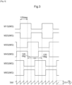
- the transformer pair (L1 and L2) for the U-phase is driven by a U-phase first switching element M1 and a U-phase second switching element M2, the transformer pair (L3 and L4) for the V-phase is driven by a V-phase first switching element M3 and a V-phase second switching element M4, and the transformer pair (L5 and L6) for the W-phase is driven by a W-phase first switching element M5 and a W-phase second switching element M6.
- the other M3G, M4G, M5G, and M6G are transformer drive signals for driving the V-phase first switching element M3, the V-phase second switching element M4, the W-phase first switching element M5, and the W-phase second switching element M6, respectively, and are a V-phase first switching element drive signal, a V-phase second switching element drive signal, a W-phase first switching element drive signal, and a W-phase second switching element drive signal, respectively.
- the U-phase second switching element drive signal M2G and the V-phase second switching element drive signal M4G are different in phase by 120° from each other, and the V-phase second switching element drive signal M4G and the W-phase second switching element drive signal M6G are also different in phase by 120° from each other, and furthermore, the W-phase second switching element drive signal M6G and the U-phase second switching element drive signal M2G are also different in phase by 120° from each other.
- the driving power supply circuit 7 includes three sets of transformer driving units 5 each including a pair of driving switching elements M: a first switching element 51 and a second switching element 52 whose switching control is complementarily performed by a pair of forward and reverse transformer drive signals having common change points.
- the present embodiment exemplifies a mode in which three transformer driving units 5 are provided, and one set of transformer driving units 5 is formed of one transformer driving unit 5.
- one set of transformer driving units 5 may be formed of a plurality of transformer driving units 5.
- a mode may be employed in which six transformer driving units 5 are provided, and one set of transformer driving units 5 is formed of two transformer driving units 5, providing three sets.
- timing at which a current ripple occurs in input current Idd on the primary side varies between the transformers L. That is, by breaking up the timing at which the input current Idd ripples, a maximum peak-to-peak I1 of ripples in the input current Idd decreases. Therefore, the maximum amplitude of current ripples on the primary side of the driving power supply circuit 7 that uses the plurality of transformers L can be reduced. As a result, for example, the size of a filter circuit that uses a filter capacitor Cf or the like that smooths out ripples in the input current Idd and thereby smooths voltage on the primary side can also be reduced.
- the plurality of transformers L are driven by the transformer drive signals MG of the same phases.
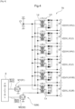
- FIG. 5 timing at which the input current Idd ripples on an input side does not vary between the transformers L, and is the same for all transformers L.
- the timing at which the input current Idd ripples is not broken up, and a maximum peak-to-peak I3 of current ripples is larger than the maximum peak-to-peak I1 exemplified in FIG. 3 .
- the maximum peak-to-peak is reduced to 1/3 that of the comparative example, by which the capacitance of the filter capacitor Cf that smooths the voltage on the primary side can be reduced, and the circuit size can also be reduced.
- the frequency of current ripples is three times that of the comparative example.
- the filter circuit is formed of a capacitor, the impedance of the capacitor is inversely proportional to frequency (with the frequency being f, the impedance is "1/2 ⁇ f"). That is, when the frequency increases, the impedance decreases and thus ripple components are more easily smoothed out.
- the above description exemplifies a mode in which the transformers L are grouped into three sets, but as a matter of course, the number (m) of sets is not limited to three.
- the transformers L may be divided into two sets: a set of upper-stage transformers LH and a set of lower-stage transformers LL.
- the transformers L may be divided into six sets in which all six transformers L belong to different groups.
- M1G and M2G are a pair of forward and reverse transformer drive signals MG for a transformer driving unit 5 that drives three upper-stage transformers LH
- M3G and M4G are a pair of forward and reverse transformer drive signals MG for a transformer driving unit 5 that drives three lower-stage transformers LL.
- a pair of forward and reverse transformer drive signals MG for a second set is delayed in phase by 45° with respect to a pair of forward and reverse transformer drive signals MG for a first set
- a pair of forward and reverse transformer drive signals MG for a third set is delayed in phase by 45° with respect to the pair of forward and reverse transformer drive signals MG for the second set
- a pair of forward and reverse transformer drive signals MG for a fourth set is delayed in phase by 45° with respect to the pair of forward and reverse transformer drive signals MG for the third set.
- the pair of forward and reverse transformer drive signals MG for the first set is delayed in phase by 225° or advanced in phase by 135° with respect to the pair of forward and reverse transformer drive signals MG for the fourth set.
- the phases of the pairs of forward and reverse transformer drive signals MG are delayed (different) by 45°with respect to each other, and when considering the fourth set, the third set, the second set, and the first set in this order, the phases of the pairs of forward and reverse transformer drive signals MG are advanced (different) by 45°with respect to each other.
- the six transformers L are grouped into three sets of transformer pairs (a pair of L1 and L2, a pair of L3 and L4, and a pair of L5 and L6) for the respective phases of three-phase alternating current.
- the transformer pairs are controlled by different transformer driving units 5 (driving switching elements M).
- FIG. 9 shows exemplary disposition of the driving power supply circuit 7 and the drive circuits 2 on a substrate.
- An upper-stage-side switching element 3H and a lower-stage-side switching element 3L for each phase are disposed in proximity to each other in disposition regions of the high-voltage system circuit HV.
- Transformers L for each phase do not supply electric power to other phases, and thus, can be disposed close to the phase.
- the transformers L for the phase are driven by driving switching elements M (transformer driving unit 5) different than those for transformers L that supply electric power to other phases. Therefore, as shown in FIG. 9 , transformers L for each phase and driving switching elements M (transformer driving unit 5) for the transformers L can be disposed in proximity to each other on a substrate 9.
- FIG. 10 shows exemplary disposition of the driving power supply circuit 70 of the comparative example exemplified in FIG. 5 and the drive circuits 2 on a substrate.
- transformers L for each phase do not supply electric power to other phases, and thus, can be disposed close to the phase.
- the transformers L for the phase are driven by the same driving switching elements M (transformer driving unit 5) as those for transformers L that supply electric power to other phases. Therefore, wiring lines between the driving switching elements M (transformer driving unit 5) and the transformers L (in FIG.
- exemplary disposition of the driving power supply circuit 7 and the drive circuits 2 on the substrate is not limited to a mode in which, as exemplified in FIG. 9 , the switching elements 3 included in the inverter 10 are arranged in a row.
- the switching elements 3 may be divided on a per alternating-current phase basis and disposed.
- the six transformers L are grouped into sets of transformers L for the respective phases of three-phase alternating current, and the sets are controlled by different transformer driving units 5 (driving switching elements M), even if the switching elements 3 are thus divided on a per alternating-current phase basis and disposed, the wiring line length between the driving switching elements M (transformer driving unit 5) and the transformers L can be shortened.
- transformers L and the driving switching elements M do not need to be disposed in proximity to each other. If transformers L and driving switching elements M (transformer driving unit 5) for at least one of the plurality of phases are disposed in proximity to each other, then an advantageous effect of a reduction in electromagnetic noise can be obtained.
- a driving power supply device (7) that supplies electric power to a plurality of drive circuits (2) that individually drive a plurality of switching elements (3) included in an inverter (10) that converts electric power between direct current and alternating current of a plurality of phases includes: a plurality of transformers (L) each including a primary-side coil (Lp) and a secondary-side coil (Ls) coupled to the primary-side coil (Lp) in an electrically isolated state, the secondary-side coils (Ls) being individually connected to the respective corresponding drive circuits (2); a plurality of transformer driving units (5) each including a driving switching element (M) that is connected to a corresponding one of the primary-side coils (Lp) and controls supply of electric power to the corresponding one of the primary-side coils (Lp); and a power supply control device (6) that provides transformer drive signals (MG) for driving the transformer driving units (5), and the power supply control device (6) drives the transformer driving units (5) by the transformer drive signals (MG) having different phases.
- m sets of the transformer driving units (5) (m is a natural number greater than or equal to 2) be provided, each set of the transformer driving units (5) being driven by the transformer drive signals (MG) having common change points, and the sets of the transformer driving units (5) be driven by the transformer drive signals (MG) whose phases are different by "360°/m" from each other.
- each transformer driving unit (5) includes a pair of the driving switching elements (M) including a first switching element (51 (M1, M3, M5)) and a second switching element (52 (M2, M4, M6)) whose switching control is complementarily performed by a pair of the forward and reverse transformer drive signals (MG) having common change points
- the sets of the transformer driving units (5) be driven as follows. Specifically, when "360/m" is a divisor of 180, it is preferred that the sets of the transformer driving units (5) be driven by pairs of the forward and reverse transformer drive signals (MG) whose phases are different by "180°/m" from each other.
- the sets of the transformer driving units (5) be driven by pairs of the forward and reverse transformer drive signals (5) whose phases are different by "360°/m" from each other.
- transformer drive signal (MG) for two driving switching elements (M) whose switching control is complementarily performed
- the logic of the other transformer drive signal (MG) is inverted. That is, switching control of two driving switching elements (M) whose switching control is complementarily performed is performed by a pair of forward and reverse transformer drive signals (MG) which is a pair of a forward signal and a reverse signal. It can be said that the phases of the pair of forward and reverse transformer drive signals (MG) are shifted by 180° relative to each other. In a case of phases whose phase difference obtained by "360°/m" is a divisor of 180°, transformer drive signals (MG) with a phase shift of 180° are generated.
- a transformer drive signal (MG) which is a forward signal included in a pair of forward and reverse transformer drive signals (MG) and a transformer drive signal (MG) which is a reverse signal included in another pair of forward and reverse transformer drive signals (MG) match each other in phase. Therefore, when "360/m” is a divisor of 180, it is desirable that the phases of a plurality of pairs of forward and reverse transformer drive signals (MG) be made different from each other in a range of 180°. On the other hand, when “360/m” is other than a divisor of 180, transformer drive signals (MG) having a phase shift of 180° are not generated. Therefore, when "360/m” is other than a divisor of 180, it is desirable that the phases of a plurality of pairs of forward and reverse transformer drive signals (MG) be made different from each other in a range of 360°.
- the inverter (10) convert electric power between n-phase alternating current (n is a natural number greater than or equal to 2) and direct current, and a number m of sets of the transformer driving units (5) be n.
- each set being driven by the transformer drive signals (MG) having common change points matches the number of phases of alternating current of a plurality of phases, grouping is easy.
- switching elements (3) for each phase are often disposed close to each other, and thus, by performing grouping phase-by-phase, efficient wiring on a substrate is also obtained.
- each transformer driving unit (5) includes a pair of the driving switching elements (M) including a first switching element (51 (M1, M3, M5)) and a second switching element (52 (M2, M4, M6)) whose switching control is complementarily performed
- M the driving switching elements
- An upper-stage-side switching element (3H) and a lower-stage-side switching element (3L) of an arm (3A) for one alternating-current phase are disposed relatively close to each other in the inverter (10). Therefore, an upper-stage-side transformer (LH) and a lower-stage-side transformer (LL) are also disposed relatively close to each other. Since a first switching element (51 (M1, M3, M5)) and a second switching element (52 (M2, M4, M6)) can also be disposed close to the upper-stage-side transformer (LH) and the lower-stage-side transformer (LL), the wiring line distance between the transformer driving unit (5) and the transformers (L) can be reduced. As described above, current ripples occur in the primary side of the transformers (L), but by shortening the wiring lines, the distance at which ripple components propagate is reduced, and electromagnetic noise occurring due to the ripple components is also reduced.
- each drive circuit (2) include an insulating element (51) that electrically isolates a low-voltage circuit (LV) including a control circuit (1) that generates switching control signals (SW) for driving the switching elements (3), from a high-voltage circuit (HV) including the inverter (10), and transmits a corresponding one of the switching control signals (SW), the upper-stage-side transformer (LH) and the lower-stage-side transformer (LL) for a same phase of alternating current be disposed adjacent to each other on a substrate (9), and corresponding ones of the insulating elements (51) for the upper-stage-side switching element (3H) and the lower-stage-side switching element (3L) for the phase be disposed on both sides in an arrangement direction with the upper-stage-side transformer (LH) and the lower-stage-side transformer (LL) sandwiched between the corresponding ones of the insulating elements (51).
- LV low-voltage circuit
- HV high-voltage circuit
- HV high-voltage circuit
- LL high-voltage circuit
- the transformers (L) are an insulating parts, and can be connected, for example, in a state in which the low-voltage circuit (LV) in which the primary-side coils (Lp) are disposed is electrically isolated from the high-voltage circuit (HV) in which the secondary-side coils (Ls) are disposed.
- the transformers (L) and the insulating elements (51) are appropriately isolated from each other, and the transformers (L) and the insulating elements (51) can be efficiently disposed.
- Inverter control device (a control circuit that generates switching control signals), 2: Drive circuit, 2H: Upper-stage-side drive circuit, 2L: Lower-stage-side drive circuit, 3: Switching element, 3A: Arm, 3H: Upper-stage-side switching element, 3L: Lower-stage-side switching element, 5: Transformer driving unit, 6: Power supply control device, 7: Driving power supply circuit (driving power supply device), 9: Substrate, 10: Inverter, 21: Insulating element, 51: First switching element, 52: Second switching element, 70: Driving power supply circuit of a comparative example, 80: Rotating electrical machine, HV: High-voltage system circuit, Idd: Input current, L: Transformer, L1: U-phase upper-stage transformer, L2: U-phase lower-stage transformer, L3: V-phase upper-stage transformer, L4: V-phase lower-stage transformer, L5: W-phase upper-stage transformer, L6: W-phase lower-stage transformer, Lp: Primary-side coil, Ls:
Landscapes
- Engineering & Computer Science (AREA)
- Power Engineering (AREA)
- Physics & Mathematics (AREA)
- Electromagnetism (AREA)
- Inverter Devices (AREA)
- Power Conversion In General (AREA)
Claims (6)
- Ansteuerenergieversorgungsvorrichtung (7), die konfiguriert ist, um eine Vielzahl von Ansteuerschaltungen (2) mit elektrischer Energie zu versorgen, die individuell eine Vielzahl von Schaltelementen (3) ansteuern, die in einem Inverter (10) enthalten sind, der konfiguriert ist, um elektrische Energie zwischen Gleichstrom und Wechselstrom einer Vielzahl von Phasen umzuwandeln, wobei die Ansteuerenergieversorgungsvorrichtung (7) aufweist:eine Vielzahl von Transformatoren (L), die jeweils ein Paar primärseitiger Spulen (Lp) und ein Paar sekundärseitiger Spulen (Ls), die mit den primärseitigen Spulen (Lp) in einem elektrisch isolierten Zustand verbunden sind, umfassen, wobei das Paar sekundärseitiger Spulen (Ls) individuell mit den jeweiligen entsprechenden Ansteuerschaltungen (2) verbunden ist;eine Vielzahl von Transformatoransteuerungseinheiten (5), die jeweils ein Paar von Ansteuerschaltelementen (M) umfassen, deren Schaltsteuerung komplementär durch ein Paar von invertierten Transformatoransteuersignalen (MG) gesteuert wird, wobei jedes Ansteuerschaltelement (M) mit einer entsprechenden Spule des Paares von primärseitigen Spulen (Lp) verbunden ist und konfiguriert ist, um eine Zufuhr von elektrischer Energie zu der entsprechenden Spule des Paares von primärseitigen Spulen (Lp) zu steuern; undeine Energieversorgungssteuervorrichtung (6), die konfiguriert ist, um die Transformatoransteuersignale (MG) zum Ansteuern der Transformatoransteuerungseinheiten (5) bereitzustellen,wobeidie Energieversorgungssteuervorrichtung (6) konfiguriert ist, um die Transformatoransteuerungseinheiten (5) durch die Transformatoransteuersignale (MG) mit unterschiedlichen Phasen anzutreiben.
- Ansteuerenergieversorgungsvorrichtung (7) gemäß Anspruch 1, wobeim Sätze der Transformatoransteuerungseinheiten (5) (m ist eine natürliche Anzahl größer als oder gleich 2) bereitgestellt sind, wobei jeder Satz der Transformatoransteuerungseinheiten (5) durch invertierte Transformatoransteuersignale (MG) angesteuert wird, unddie Sätze der Transformatoransteuerungseinheiten (5) durch die Transformatoransteuersignale (MG) angesteuert werden, deren Phasen sich um "360°/m" voneinander unterscheiden.
- Ansteuerenergieversorgungsvorrichtung (7) gemäß Anspruch 2, wobeijede Transformatoransteuerungseinheit (5) das Paar der Ansteuerschaltelemente (M) umfasst, das ein erstes Schaltelement (51 (M1, M3, M5)) und ein zweites Schaltelement (52 (M2, M4, M6)) umfasst,wenn "360/m" ein Teiler von 180 ist, die Sätze der Transformatoransteuerungseinheiten (5) durch Paare der invertierten Transformatoransteuersignale (MG) angesteuert werden, deren Phasen sich um "180°/m" voneinander unterscheiden, undwenn "360/m" sich von einem Teiler von 180 unterscheidet, die Sätze der Transformatoransteuerungseinheiten (5) durch Paare der invertierten Transformatoransteuersignale (MG) angesteuert werden, deren Phasen sich um "360°/m" voneinander unterscheiden.
- Ansteuerenergieversorgungsvorrichtung (7) gemäß Anspruch 2 oder 3, wobei der Inverter (10) konfiguriert ist, um elektrische Energie zwischen n-phasigem Wechselstrom (n ist eine natürliche Zahl größer oder gleich 2) und Gleichstrom zu konvertieren, und eine Anzahl m von Sätzen der Transformatoransteuerungseinheiten (5) n ist.
- Ansteuerenergieversorgungsvorrichtung (7) gemäß einem der Ansprüche 1 bis 4, wobeider Inverter (10) eine Vielzahl von Zweigen (3A) für jeweils eine Wechselstromphase umfasst, wobei jeder Zweig (3A) eine Reihenschaltung aus einem oberstufenseitigen Schaltelement (3H), das mit einer positiven Polaritätsseite von Gleichstrom verbunden ist, und einem unterstufenseitigen Schaltelement (3L), das mit einer negativen Polaritätsseite von Gleichstrom verbunden ist, darstellt,jede Transformatoransteuerungseinheit (5) ein Paar der Ansteuerschaltelemente (M) umfasst, das ein erstes Schaltelement (51 (M1, M3, M5)) und ein zweites Schaltelement (52 (M2, M4, M6)) umfasst, deren Schaltsteuerung komplementär gesteuert wird,von der Vielzahl von Transformatoren (L) ein oberstufenseitiger Transformator (LH) und ein unterstufenseitiger Transformator (LL) für eine gleiche Wechselstromphase von der gemeinsamen Transformatoransteuerungseinheit (5) angesteuert werden, wobei der oberstufenseitige Transformator (LH) einer Oberstufenseite einem der Zweige (3A) entspricht und der unterstufenseitige Transformator (LL) einer Unterstufenseite entspricht,ein Ende einer entsprechenden der primärseitigen Spulen (Lp) des oberstufenseitigen Transformators (LH) und ein Ende einer entsprechenden der primärseitigen Spulen (Lp) des unterstufenseitigen Transformators (LL) mit einem entsprechenden der ersten Schaltelemente (51 (M1, M3, M5)) verbunden sind, undein anderes Ende der entsprechenden primärseitigen Spulen (Lp) des oberseitigen Transformators (LH) und ein anderes Ende der entsprechenden primärseitigen Spulen (Lp) des unterseitigen Transformators (LL) mit einem entsprechenden der zweiten Schaltelemente (52 (M2, M4, M6)) verbunden sind.
- Ansteuerenergieversorgungsvorrichtung (7) gemäß Anspruch 5, wobeijede Ansteuerschaltung (2) ein Isolierelement (51) umfasst, das eine Niederspannungs-Systemschaltung (LV), die eine Steuerschaltung (1) umfasst, die konfiguriert ist, um Schaltsteuersignale (SW) zum Steuern der Schaltelemente (3) zu erzeugen, von einer Hochspannungs-Systemschaltung (HV), die den Inverter (10) umfasst, elektrisch isoliert und ein entsprechendes der Schaltsteuersignale (SW) überträgt,der oberstufenseitige Transformator (LH) und der unterstufenseitige Transformator (LL) für eine gleiche Wechselstromphase nebeneinander auf einem Substrat (9) angeordnet sind, undentsprechende der Isolierelemente (51) für das oberstufenseitige Schaltelement (3H) und das unterstufenseitige Schaltelement (3L) für die Phase auf beiden Seiten in einer Anordnungsrichtung angeordnet sind, wobei der oberstufenseitige Transformator (LH) und der unterstufenseitige Transformator (LL) sandwichartig zwischen den entsprechenden der Isolierelemente (51) angeordnet sind.
Applications Claiming Priority (2)
| Application Number | Priority Date | Filing Date | Title |
|---|---|---|---|
| JP2017180145 | 2017-09-20 | ||
| PCT/JP2018/034859 WO2019059292A1 (ja) | 2017-09-20 | 2018-09-20 | 駆動電源装置 |
Publications (3)
| Publication Number | Publication Date |
|---|---|
| EP3651341A1 EP3651341A1 (de) | 2020-05-13 |
| EP3651341A4 EP3651341A4 (de) | 2020-07-15 |
| EP3651341B1 true EP3651341B1 (de) | 2024-12-25 |
Family
ID=65810309
Family Applications (1)
| Application Number | Title | Priority Date | Filing Date |
|---|---|---|---|
| EP18859203.4A Active EP3651341B1 (de) | 2017-09-20 | 2018-09-20 | Antriebsleistungversorgungsvorrichtung |
Country Status (5)
| Country | Link |
|---|---|
| US (1) | US11070163B2 (de) |
| EP (1) | EP3651341B1 (de) |
| JP (1) | JP6763487B2 (de) |
| CN (1) | CN111095767B (de) |
| WO (1) | WO2019059292A1 (de) |
Families Citing this family (7)
| Publication number | Priority date | Publication date | Assignee | Title |
|---|---|---|---|---|
| CN111095768B (zh) * | 2017-09-27 | 2023-04-18 | 株式会社爱信 | 逆变器模块 |
| US11349410B2 (en) * | 2018-01-30 | 2022-05-31 | Mitsubishi Electric Corporation | Series multiplex inverter |
| US12249924B2 (en) | 2019-08-23 | 2025-03-11 | Mitsubishi Electric Corporation | Power conversion control device |
| CN114365410B (zh) * | 2019-11-25 | 2025-10-14 | 株式会社爱信 | 控制基板 |
| JP7584034B2 (ja) * | 2020-01-31 | 2024-11-15 | パナソニックIpマネジメント株式会社 | D級電力変換器 |
| US20210257927A1 (en) * | 2020-02-13 | 2021-08-19 | Delta Electronics, Inc. | Inverter system |
| CN118947053A (zh) * | 2022-03-25 | 2024-11-12 | 罗姆股份有限公司 | 驱动装置、开关电源装置以及车辆 |
Family Cites Families (10)
| Publication number | Priority date | Publication date | Assignee | Title |
|---|---|---|---|---|
| US4150425A (en) * | 1978-02-09 | 1979-04-17 | Nasa | Module failure isolation circuit for paralleled inverters |
| JP3375893B2 (ja) * | 1998-08-28 | 2003-02-10 | 長野日本無線株式会社 | スイッチング電源用ドライブ回路 |
| JP5029900B2 (ja) * | 2007-11-20 | 2012-09-19 | アイシン・エィ・ダブリュ株式会社 | モータの制御装置 |
| JP5272638B2 (ja) * | 2008-10-15 | 2013-08-28 | トヨタ自動車株式会社 | スイッチング電源装置及びスイッチング制御システム |
| JP5252219B2 (ja) * | 2009-05-26 | 2013-07-31 | アイシン・エィ・ダブリュ株式会社 | インバータ駆動用電源回路 |
| JP4831246B2 (ja) * | 2009-09-08 | 2011-12-07 | 株式会社デンソー | 電力変換装置 |
| JP5622043B2 (ja) * | 2010-09-15 | 2014-11-12 | アイシン・エィ・ダブリュ株式会社 | インバータ装置 |
| JP5510292B2 (ja) * | 2010-11-30 | 2014-06-04 | 富士電機株式会社 | ゲート駆動用電源装置およびインバータ制御回路 |
| JP6191478B2 (ja) * | 2014-01-28 | 2017-09-06 | アイシン・エィ・ダブリュ株式会社 | 電力変換装置 |
| JP6172061B2 (ja) * | 2014-06-12 | 2017-08-02 | 株式会社デンソー | 電力変換回路用の電源装置 |
-
2018
- 2018-09-20 US US16/637,805 patent/US11070163B2/en active Active
- 2018-09-20 EP EP18859203.4A patent/EP3651341B1/de active Active
- 2018-09-20 WO PCT/JP2018/034859 patent/WO2019059292A1/ja not_active Ceased
- 2018-09-20 JP JP2019543701A patent/JP6763487B2/ja active Active
- 2018-09-20 CN CN201880057730.1A patent/CN111095767B/zh active Active
Also Published As
| Publication number | Publication date |
|---|---|
| JP6763487B2 (ja) | 2020-09-30 |
| US20200220489A1 (en) | 2020-07-09 |
| EP3651341A4 (de) | 2020-07-15 |
| US11070163B2 (en) | 2021-07-20 |
| JPWO2019059292A1 (ja) | 2020-03-26 |
| CN111095767A (zh) | 2020-05-01 |
| WO2019059292A1 (ja) | 2019-03-28 |
| CN111095767B (zh) | 2023-10-27 |
| EP3651341A1 (de) | 2020-05-13 |
Similar Documents
| Publication | Publication Date | Title |
|---|---|---|
| EP3651341B1 (de) | Antriebsleistungversorgungsvorrichtung | |
| US11258391B2 (en) | Rotating electrical machine control device | |
| WO2021076859A1 (en) | Multibridge power converter with multiple outputs | |
| JP6087666B2 (ja) | 電力変換装置 | |
| US9467086B2 (en) | Vehicle-mounted motor driving control board | |
| US9379597B2 (en) | System for driving electromagnetic appliance and motor driven vehicle | |
| US6831442B2 (en) | Utilizing zero-sequence switchings for reversible converters | |
| US9621100B2 (en) | Vehicular AC electric generator | |
| US20080258661A1 (en) | Inverter topology for an electric motor | |
| CN111213312B (zh) | 逆变器控制基板 | |
| US12027908B2 (en) | High power density universal vehicle charger | |
| JP2010284029A (ja) | インバータ駆動用電源回路 | |
| WO2018055792A1 (ja) | 電力変換装置 | |
| WO2015115226A1 (ja) | 電力変換装置 | |
| JP2008236889A (ja) | インバータ装置 | |
| KR101654755B1 (ko) | 교류 모터 또는 직류 모터의 선택적 제어 | |
| JP2010283934A (ja) | 三相交流電動機の制御装置 | |
| EP4679698A1 (de) | Leistungsumwandlungsvorrichtung und verfahren zur steuerung davon | |
| JP2024104700A (ja) | 充電制御方法、充電制御装置、及び、電源回路 | |
| JP2021035225A (ja) | 制御基板 |
Legal Events
| Date | Code | Title | Description |
|---|---|---|---|
| STAA | Information on the status of an ep patent application or granted ep patent |
Free format text: STATUS: THE INTERNATIONAL PUBLICATION HAS BEEN MADE |
|
| PUAI | Public reference made under article 153(3) epc to a published international application that has entered the european phase |
Free format text: ORIGINAL CODE: 0009012 |
|
| STAA | Information on the status of an ep patent application or granted ep patent |
Free format text: STATUS: REQUEST FOR EXAMINATION WAS MADE |
|
| 17P | Request for examination filed |
Effective date: 20200205 |
|
| AK | Designated contracting states |
Kind code of ref document: A1 Designated state(s): AL AT BE BG CH CY CZ DE DK EE ES FI FR GB GR HR HU IE IS IT LI LT LU LV MC MK MT NL NO PL PT RO RS SE SI SK SM TR |
|
| AX | Request for extension of the european patent |
Extension state: BA ME |
|
| STAA | Information on the status of an ep patent application or granted ep patent |
Free format text: STATUS: EXAMINATION IS IN PROGRESS |
|
| A4 | Supplementary search report drawn up and despatched |
Effective date: 20200617 |
|
| RIC1 | Information provided on ipc code assigned before grant |
Ipc: H03K 17/567 20060101ALI20200610BHEP Ipc: H02M 7/48 20070101AFI20200610BHEP Ipc: H02M 1/08 20060101ALI20200610BHEP Ipc: H03K 17/78 20060101ALI20200610BHEP Ipc: H02M 3/335 20060101ALI20200610BHEP Ipc: H03K 17/691 20060101ALI20200610BHEP |
|
| 17Q | First examination report despatched |
Effective date: 20200703 |
|
| DAV | Request for validation of the european patent (deleted) | ||
| DAX | Request for extension of the european patent (deleted) | ||
| RAP1 | Party data changed (applicant data changed or rights of an application transferred) |
Owner name: AISIN CORPORATION |
|
| GRAP | Despatch of communication of intention to grant a patent |
Free format text: ORIGINAL CODE: EPIDOSNIGR1 |
|
| STAA | Information on the status of an ep patent application or granted ep patent |
Free format text: STATUS: GRANT OF PATENT IS INTENDED |
|
| INTG | Intention to grant announced |
Effective date: 20240726 |
|
| RIN1 | Information on inventor provided before grant (corrected) |
Inventor name: SEKIGUCHI, SHOTA Inventor name: ITO, YOSHINOBU Inventor name: MUTSUURA, KEITA Inventor name: NAKAMURA, YASUSHI |
|
| GRAS | Grant fee paid |
Free format text: ORIGINAL CODE: EPIDOSNIGR3 |
|
| GRAA | (expected) grant |
Free format text: ORIGINAL CODE: 0009210 |
|
| STAA | Information on the status of an ep patent application or granted ep patent |
Free format text: STATUS: THE PATENT HAS BEEN GRANTED |
|
| AK | Designated contracting states |
Kind code of ref document: B1 Designated state(s): AL AT BE BG CH CY CZ DE DK EE ES FI FR GB GR HR HU IE IS IT LI LT LU LV MC MK MT NL NO PL PT RO RS SE SI SK SM TR |
|
| REG | Reference to a national code |
Ref country code: GB Ref legal event code: FG4D |
|
| REG | Reference to a national code |
Ref country code: CH Ref legal event code: EP |
|
| REG | Reference to a national code |
Ref country code: DE Ref legal event code: R096 Ref document number: 602018078003 Country of ref document: DE |
|
| REG | Reference to a national code |
Ref country code: IE Ref legal event code: FG4D |
|
| REG | Reference to a national code |
Ref country code: LT Ref legal event code: MG9D |
|
| PG25 | Lapsed in a contracting state [announced via postgrant information from national office to epo] |
Ref country code: HR Free format text: LAPSE BECAUSE OF FAILURE TO SUBMIT A TRANSLATION OF THE DESCRIPTION OR TO PAY THE FEE WITHIN THE PRESCRIBED TIME-LIMIT Effective date: 20241225 |
|
| PG25 | Lapsed in a contracting state [announced via postgrant information from national office to epo] |
Ref country code: FI Free format text: LAPSE BECAUSE OF FAILURE TO SUBMIT A TRANSLATION OF THE DESCRIPTION OR TO PAY THE FEE WITHIN THE PRESCRIBED TIME-LIMIT Effective date: 20241225 |
|
| PG25 | Lapsed in a contracting state [announced via postgrant information from national office to epo] |
Ref country code: BG Free format text: LAPSE BECAUSE OF FAILURE TO SUBMIT A TRANSLATION OF THE DESCRIPTION OR TO PAY THE FEE WITHIN THE PRESCRIBED TIME-LIMIT Effective date: 20241225 |
|
| PG25 | Lapsed in a contracting state [announced via postgrant information from national office to epo] |
Ref country code: NO Free format text: LAPSE BECAUSE OF FAILURE TO SUBMIT A TRANSLATION OF THE DESCRIPTION OR TO PAY THE FEE WITHIN THE PRESCRIBED TIME-LIMIT Effective date: 20250325 |
|
| PG25 | Lapsed in a contracting state [announced via postgrant information from national office to epo] |
Ref country code: LV Free format text: LAPSE BECAUSE OF FAILURE TO SUBMIT A TRANSLATION OF THE DESCRIPTION OR TO PAY THE FEE WITHIN THE PRESCRIBED TIME-LIMIT Effective date: 20241225 Ref country code: GR Free format text: LAPSE BECAUSE OF FAILURE TO SUBMIT A TRANSLATION OF THE DESCRIPTION OR TO PAY THE FEE WITHIN THE PRESCRIBED TIME-LIMIT Effective date: 20250326 |
|
| PG25 | Lapsed in a contracting state [announced via postgrant information from national office to epo] |
Ref country code: RS Free format text: LAPSE BECAUSE OF FAILURE TO SUBMIT A TRANSLATION OF THE DESCRIPTION OR TO PAY THE FEE WITHIN THE PRESCRIBED TIME-LIMIT Effective date: 20250325 |
|
| REG | Reference to a national code |
Ref country code: NL Ref legal event code: MP Effective date: 20241225 |
|
| PG25 | Lapsed in a contracting state [announced via postgrant information from national office to epo] |
Ref country code: NL Free format text: LAPSE BECAUSE OF FAILURE TO SUBMIT A TRANSLATION OF THE DESCRIPTION OR TO PAY THE FEE WITHIN THE PRESCRIBED TIME-LIMIT Effective date: 20241225 |
|
| REG | Reference to a national code |
Ref country code: AT Ref legal event code: MK05 Ref document number: 1755023 Country of ref document: AT Kind code of ref document: T Effective date: 20241225 |
|
| PG25 | Lapsed in a contracting state [announced via postgrant information from national office to epo] |
Ref country code: SM Free format text: LAPSE BECAUSE OF FAILURE TO SUBMIT A TRANSLATION OF THE DESCRIPTION OR TO PAY THE FEE WITHIN THE PRESCRIBED TIME-LIMIT Effective date: 20241225 |
|
| PG25 | Lapsed in a contracting state [announced via postgrant information from national office to epo] |
Ref country code: PL Free format text: LAPSE BECAUSE OF FAILURE TO SUBMIT A TRANSLATION OF THE DESCRIPTION OR TO PAY THE FEE WITHIN THE PRESCRIBED TIME-LIMIT Effective date: 20241225 |
|
| PG25 | Lapsed in a contracting state [announced via postgrant information from national office to epo] |
Ref country code: ES Free format text: LAPSE BECAUSE OF FAILURE TO SUBMIT A TRANSLATION OF THE DESCRIPTION OR TO PAY THE FEE WITHIN THE PRESCRIBED TIME-LIMIT Effective date: 20241225 |
|
| PG25 | Lapsed in a contracting state [announced via postgrant information from national office to epo] |
Ref country code: IS Free format text: LAPSE BECAUSE OF FAILURE TO SUBMIT A TRANSLATION OF THE DESCRIPTION OR TO PAY THE FEE WITHIN THE PRESCRIBED TIME-LIMIT Effective date: 20250425 |
|
| PG25 | Lapsed in a contracting state [announced via postgrant information from national office to epo] |
Ref country code: PT Free format text: LAPSE BECAUSE OF FAILURE TO SUBMIT A TRANSLATION OF THE DESCRIPTION OR TO PAY THE FEE WITHIN THE PRESCRIBED TIME-LIMIT Effective date: 20250428 |
|
| PG25 | Lapsed in a contracting state [announced via postgrant information from national office to epo] |
Ref country code: EE Free format text: LAPSE BECAUSE OF FAILURE TO SUBMIT A TRANSLATION OF THE DESCRIPTION OR TO PAY THE FEE WITHIN THE PRESCRIBED TIME-LIMIT Effective date: 20241225 |
|
| PG25 | Lapsed in a contracting state [announced via postgrant information from national office to epo] |
Ref country code: RO Free format text: LAPSE BECAUSE OF FAILURE TO SUBMIT A TRANSLATION OF THE DESCRIPTION OR TO PAY THE FEE WITHIN THE PRESCRIBED TIME-LIMIT Effective date: 20241225 Ref country code: AT Free format text: LAPSE BECAUSE OF FAILURE TO SUBMIT A TRANSLATION OF THE DESCRIPTION OR TO PAY THE FEE WITHIN THE PRESCRIBED TIME-LIMIT Effective date: 20241225 |
|
| PG25 | Lapsed in a contracting state [announced via postgrant information from national office to epo] |
Ref country code: SK Free format text: LAPSE BECAUSE OF FAILURE TO SUBMIT A TRANSLATION OF THE DESCRIPTION OR TO PAY THE FEE WITHIN THE PRESCRIBED TIME-LIMIT Effective date: 20241225 |
|
| PG25 | Lapsed in a contracting state [announced via postgrant information from national office to epo] |
Ref country code: CZ Free format text: LAPSE BECAUSE OF FAILURE TO SUBMIT A TRANSLATION OF THE DESCRIPTION OR TO PAY THE FEE WITHIN THE PRESCRIBED TIME-LIMIT Effective date: 20241225 |
|
| PG25 | Lapsed in a contracting state [announced via postgrant information from national office to epo] |
Ref country code: IT Free format text: LAPSE BECAUSE OF FAILURE TO SUBMIT A TRANSLATION OF THE DESCRIPTION OR TO PAY THE FEE WITHIN THE PRESCRIBED TIME-LIMIT Effective date: 20241225 |
|
| PG25 | Lapsed in a contracting state [announced via postgrant information from national office to epo] |
Ref country code: SE Free format text: LAPSE BECAUSE OF FAILURE TO SUBMIT A TRANSLATION OF THE DESCRIPTION OR TO PAY THE FEE WITHIN THE PRESCRIBED TIME-LIMIT Effective date: 20241225 |
|
| REG | Reference to a national code |
Ref country code: DE Ref legal event code: R097 Ref document number: 602018078003 Country of ref document: DE |
|
| PG25 | Lapsed in a contracting state [announced via postgrant information from national office to epo] |
Ref country code: DK Free format text: LAPSE BECAUSE OF FAILURE TO SUBMIT A TRANSLATION OF THE DESCRIPTION OR TO PAY THE FEE WITHIN THE PRESCRIBED TIME-LIMIT Effective date: 20241225 |
|
| PGFP | Annual fee paid to national office [announced via postgrant information from national office to epo] |
Ref country code: DE Payment date: 20250730 Year of fee payment: 8 |
|
| PGFP | Annual fee paid to national office [announced via postgrant information from national office to epo] |
Ref country code: GB Payment date: 20250731 Year of fee payment: 8 |
|
| PGFP | Annual fee paid to national office [announced via postgrant information from national office to epo] |
Ref country code: FR Payment date: 20250808 Year of fee payment: 8 |
|
| PLBE | No opposition filed within time limit |
Free format text: ORIGINAL CODE: 0009261 |
|
| STAA | Information on the status of an ep patent application or granted ep patent |
Free format text: STATUS: NO OPPOSITION FILED WITHIN TIME LIMIT |
|
| 26N | No opposition filed |
Effective date: 20250926 |