EP3655721B1 - Erzeugung von strukturiertem licht - Google Patents
Erzeugung von strukturiertem licht Download PDFInfo
- Publication number
- EP3655721B1 EP3655721B1 EP18780208.7A EP18780208A EP3655721B1 EP 3655721 B1 EP3655721 B1 EP 3655721B1 EP 18780208 A EP18780208 A EP 18780208A EP 3655721 B1 EP3655721 B1 EP 3655721B1
- Authority
- EP
- European Patent Office
- Prior art keywords
- pattern
- light
- emitted
- light emitting
- emitting devices
- Prior art date
- Legal status (The legal status is an assumption and is not a legal conclusion. Google has not performed a legal analysis and makes no representation as to the accuracy of the status listed.)
- Active
Links
Images



Classifications
-
- G—PHYSICS
- G02—OPTICS
- G02B—OPTICAL ELEMENTS, SYSTEMS OR APPARATUS
- G02B27/00—Optical systems or apparatus not provided for by any of the groups G02B1/00 - G02B26/00, G02B30/00
- G02B27/42—Diffraction optics, i.e. systems including a diffractive element being designed for providing a diffractive effect
- G02B27/4233—Diffraction optics, i.e. systems including a diffractive element being designed for providing a diffractive effect having a diffractive element [DOE] contributing to a non-imaging application
- G02B27/425—Diffraction optics, i.e. systems including a diffractive element being designed for providing a diffractive effect having a diffractive element [DOE] contributing to a non-imaging application in illumination systems
-
- G—PHYSICS
- G01—MEASURING; TESTING
- G01B—MEASURING LENGTH, THICKNESS OR SIMILAR LINEAR DIMENSIONS; MEASURING ANGLES; MEASURING AREAS; MEASURING IRREGULARITIES OF SURFACES OR CONTOURS
- G01B11/00—Measuring arrangements characterised by the use of optical techniques
- G01B11/24—Measuring arrangements characterised by the use of optical techniques for measuring contours or curvatures
- G01B11/25—Measuring arrangements characterised by the use of optical techniques for measuring contours or curvatures by projecting a pattern, e.g. one or more lines, moiré fringes on the object
- G01B11/2513—Measuring arrangements characterised by the use of optical techniques for measuring contours or curvatures by projecting a pattern, e.g. one or more lines, moiré fringes on the object with several lines being projected in more than one direction, e.g. grids, patterns
-
- G—PHYSICS
- G02—OPTICS
- G02B—OPTICAL ELEMENTS, SYSTEMS OR APPARATUS
- G02B27/00—Optical systems or apparatus not provided for by any of the groups G02B1/00 - G02B26/00, G02B30/00
- G02B27/09—Beam shaping, e.g. changing the cross-sectional area, not otherwise provided for
- G02B27/0905—Dividing and/or superposing multiple light beams
-
- G—PHYSICS
- G02—OPTICS
- G02B—OPTICAL ELEMENTS, SYSTEMS OR APPARATUS
- G02B27/00—Optical systems or apparatus not provided for by any of the groups G02B1/00 - G02B26/00, G02B30/00
- G02B27/42—Diffraction optics, i.e. systems including a diffractive element being designed for providing a diffractive effect
- G02B27/4272—Diffraction optics, i.e. systems including a diffractive element being designed for providing a diffractive effect having plural diffractive elements positioned sequentially along the optical path
- G02B27/4277—Diffraction optics, i.e. systems including a diffractive element being designed for providing a diffractive effect having plural diffractive elements positioned sequentially along the optical path being separated by an air space
-
- G—PHYSICS
- G02—OPTICS
- G02B—OPTICAL ELEMENTS, SYSTEMS OR APPARATUS
- G02B13/00—Optical objectives specially designed for the purposes specified below
- G02B13/22—Telecentric objectives or lens systems
Definitions
- the present invention relates generally to light projection systems, and apparatuses and their use for generating structured light patterns.
- Light projection systems are used in a variety of applications to cast a pattern of light upon a surface.
- known light projection systems can be used in determining the three-dimensional (3D) shape of objects.
- 3D shape measurement or 3D mapping
- a structured light pattern is first projected onto the object surface.
- An image of the fringe pattern that is phase modulated by the object height distribution is recorded, and then used to calculate the phase modulation, to which an algorithm is applied to obtain a phase distribution proportional to the object height variations.
- real world coordinates are constructed.
- it is advantageous to use a structured light pattern that is an irregular pattern in a method for 3D shape measurement because of the subsequent calculation of phase modulation and determination of phase distribution.
- Previous light projections system used in 3D shape measurement comprise light emitting elements, which can be light-emitting diodes (LEDs) or vertical-cavity surface-emitting laser (VCSEL) diodes, and a means to project the emitted light pattern onto a surface.
- Light projection systems can use a projection lens or additional optical elements to project the emitted light pattern onto a surface, or alter and then project the emitted light pattern onto a surface.
- Such optical elements can be a diffractive optical element (DOE). DOEs are configured to diffract an incoming beam or pattern of light to generate an output pattern in a predetermined way.
- DOE diffractive optical element
- an incoming beam or pattern of light can be collimated, or be shaped into a different intensity pattern and with a lower output energy than the incoming beam or pattern of light.
- US 2016/178915 A1 describes a device having an array of optical emitters arranged in a two-dimensional pattern, a projection lens, and a DOE.
- US 2013/044187 A1 describes an illumination unit having a light source and an upstream microoptical array to produce an illumination pattern.
- US 2010/284082 A1 describes an optical apparatus having first and second DOEs arranged in series to diffract an input beam of radiation.
- an irregular light pattern provides advantages in a method for 3D shape measurement.
- manufacturing an array of light configured to produce an irregular light pattern is costly.
- the present invention provides a structured light system that does not require an irregular array of light emitting devices, but instead, relies on an optical element to create an irregular emitted light pattern from an array of light emitting devices that emit a regular pattern.
- an optical element to achieve an irregular pattern of light not only avoids the costs associated with manufacturing an irregular array of light emitting devices, but also demonstrates advantages over other alternative solutions for producing an irregular pattern of light.
- an array of light configured to produce a regular pattern of light and selectively choose which light emitting devices in the array to toggle on or off in order to produce an irregular pattern of light; however, this alternative would disadvantageously increase the power consumed by the structured light system.
- the structured light projection system of the present invention includes an array of light emitting devices, which can be configured to emit a pattern of light.
- the pattern of light is received by a first optical element, which is configured to alter the pattern of light to generate a first emitted pattern of light that is irregular.
- the first emitted pattern of light can then be transmitted to a second optical element, which is configured to receive the first pattern of light and reproduce the first emitted pattern along a second emitted pattern, which comprises multiple instances of the first emitted pattern arranged in a tiled pattern.
- the structured light projection system of the present invention may be used for generating a structured light pattern.
- Embodiments of the systems and methods described can include one or more of the following features. Unless otherwise stated, any of the various features can be included or implemented in any combination with one another in the systems and methods described below.
- the systems and methods can further comprise a projection lens system configured to receive light emitted from the array of light emitting devices and project the light to the first optical element.
- the array of light emitting devices comprises a grid of light emitting devices.
- the grid can comprise a 12 by 9 grid of light emitting devices.
- the light emitting devices comprise VCSELs.
- the first emitted pattern comprises an irregular pattern
- the second emitted pattern comprises a uniform distribution of the irregular pattern
- the pattern of light emitted by the light emitting devices comprises a grid of individual clusters of light emitting devices, the individual clusters of light emitting devices comprising light emitting devices arranged in a non-uniform pattern.
- adjacent clusters of light emitting devices can comprise light emitting devices arranged in a common non-uniform pattern.
- adjacent clusters of light emitting devices can comprise light emitting devices arranged in differing non-uniform patterns.
- the adjacent clusters of light emitting devices are arranged in a sequence of differing non-uniform patterns, the sequence being reproduced, or repeated, at least once.
- the tiled pattern comprises adjacent instances of the first emitted patterns at least partially overlapping with one another.
- overlapping patterns include at least one element of a first pattern instance being disposed within or between multiple elements of a second pattern instance.
- at least some portions of the individual instances can be unobstructed by an adjacent instance. That is, in some cases, adjacent instances (e.g., tiles) can partially overlap one another yet remain substantially distinct or unaltered by surrounding tiles.
- overlapping instances or tiles can each be at least about 20% (e.g., at least about 30%, 40%, 50%, 60%, 70%, 80%, 90%, 95%) non-overlapping, where the non-overlapping portions of tiles are representative of the pattern of light provided to the second optical element (e.g., the first pattern).
- interlaced tiles can include a central non-overlapping portion and an outer overlapping portion (e.g., an overlapping border) that overlaps with an outer overlapping portion of an adjacent tile.
- the tiled pattern comprises adjacent instances of the first emitted patterns separate from one another.
- the tiled pattern comprises an arrangement of the first emitted pattern arranged in a series of columns and rows. In some examples, the arrangement comprises a 3 by 3 matrix. In some examples, the arrangement comprises a 2 by 2 matrix.
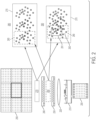
- FIG. 1 illustrates an example of a structured light projection system.
- an array of light emitting devices 100 emits a pattern of light.
- the light array 100 comprises a group of three, 12 by 9 grids of VSCELs, or a total of 324 VCSELs.
- the pitch of the light array can be 40 micrometers (p.m), and can be potentially reduced to as low as 20 p.m.
- the light array can be in a staggered layout.
- a projection lens system 110 with a projection lens 120, is configured to receive light emitted from the array of light emitting devices and project the light to a first optical element 130.
- the first optical element 130 alters the pattern of light emitted by the light array 100 to generate a first emitted pattern of light. In this alteration, the first optical element 130 splits each light emitting device in the light array 100 into a given number of irregular, encoded dot positions.
- the first emitted pattern of light is received by the second optical element 140, which is configured to reproduce the first emitted pattern along a second emitted pattern.
- the second pattern comprises multiple instances of the first emitted pattern arranged in a tiled pattern, which can form an irregular projected dot pattern 150.
- the irregular projected dot pattern 150 produced by the second optical element 140 covers the full field of illumination.
- the first optical element 130 splits each light emitting device into 12 dot positions when the tiled pattern comprises a 2 by 2 matrix, or 30 dot positions when the tiled pattern comprises a 3 by 3 matrix.
- the irregular projected dot pattern 150 comprises approximately 32,000 dots, with each unit cell size comprising between 30 to 80 dots.
- the example system of FIG. 1 can be used to carry out any of the various methods described herein. Additionally, the example systems illustrated and described herein can be manufactured using the manufacturing methods described herein.
- FIG. 2 illustrates example light patterns that can be generated and projected by the example structured light projection systems described herein.
- the light array 200 in FIG. 2 corresponds to the light array 100 in FIG. 1 ;
- the projection lens system 210 in FIG. 2 corresponds to the projection lens system 110 in FIG. 1 ;
- the projection lens 220 in FIG. 2 corresponds to the projection lens 120 in FIG. 1 .
- the first optical element 230 upon receiving the light emitted from the light array 200 by way of the projection lens system 210, can generate a first pattern of light 260, which can be an irregular pattern.
- Example first patterns of light can be a tiled multiplication pattern 280 or an interlaced multiplication pattern 290.
- the second optical element 240 can reproduce the first pattern of light 260 to create multiple instances of the first pattern of light 260, forming a second pattern of light 270.
- the second pattern of light 270 can form the irregular projected dot pattern 250 projected from the structured light projection system.
- the second pattern of light 270 is an interlaced multiplication pattern 290
- FIGS. 3A-3C illustrate three different example embodiments for light patterns that can be generated using the systems and methods described herein.
- FIG. 3A depicts illustrative examples, which are not according to the present invention, in which the light array projects a regular (e.g., grid) pattern of light.
- regular or grid can include repeated or consistent patterns of light emitting elements.
- the regular pattern 301 includes columns and rows of light emitting elements that are arranged generally perpendicularly relative to one another.
- the regular pattern of light can include an angled regular (e.g., slanted or rhombus-like) pattern 302. That is, in some embodiments, the regular pattern includes columns and rows of light emitting elements in which rows can be angled, or non-perpendicular, with respect to the direction of columns.
- FIG. 3B depict examples in which the array projects a regular pattern of a sub pattern of lights.
- the sub pattern of lights comprises smaller clusters of light.
- the regular pattern 311 includes columns and rows of clusters of light emitting elements that are arranged generally perpendicularly relative to one another.
- the regular pattern of light can include an angled regular (e.g., slanted or rhombus-like) pattern 312 comprising clusters of lights. That is, in some embodiments, the regular pattern includes columns and rows of clusters of light emitting elements in which rows can be angled, or non-perpendicular, with respect to the direction of columns.
- FIG. 3C depicts an example in which the array projects a regular pattern of a sub pattern of lights (e.g., a grid of smaller clusters of light) that can have differently shaped clusters in one direction of the grid 321 (e.g., along rows of the x-axis) and commonly shaped clusters in one direction of the grid 322 (e.g., along columns or the y-axis).
- a regular pattern of a sub pattern of lights e.g., a grid of smaller clusters of light
- the grid can have a sequence of differently shaped clusters 323 from column to column (e.g., marked A, B, and C in Figure 3C ).
- the sequence of differently shaped clusters along a row can be repeated (e.g., A, B, C, A, B, C, etc.).
- FIG. 4 depicts an example projection lens system between an object plane 401 and an image plane 402.
- the projection lens system can include one or more optical components that project light from the light emitting elements. Any of various configurations are possible.
- the projection lens can include one or more lens elements.
- the projections lens, or the one or more lens elements forming the projection lens can be formed by any of various suitable manufacturing techniques.
- the projection lens can be fabricated by injection molding or wafer-level manufacturing techniques.
- the projection lens can have an effective focal length that is less than or equal to about 5 millimeters (mm) (e.g., about 1.5 mm to about 5 mm). In some embodiments, the projection lens can have an object field height that is less than or equal to about 1 mm (e.g., about 0.2 mm to about 1.0 mm).
- a lens element can be telecentric on an object side of the projection lens, with no system aperture.
- arrangements can include non-telecentric designs (e.g., chief ray angle (CRA) ⁇ > 0 deg) and use one or more system apertures.
- CRA chief ray angle
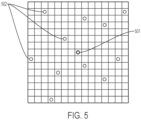
- FIG. 5 depicts an example optical element that can be used with the systems and methods herein.
- the optical element can be used to create irregular or randomized patterns of light from the light produced by the regular array, which can be a regular light pattern.
- the optical element can be a diffractive optical element.
- a diffractive optical element can include a diffraction grating, typically a 2-dimensional grating, which splits an incoming beam 501.
- the incoming beam entering the diffractive optical element can be emitted from a single light emitting element, such as a VCSEL, after having been collimated by the projection optics, such as the projection lens.
- the diffractive optical element can be formed in any of various suitable constructions.
- the diffractive optical element can be formed as a binary transmission mask.
- the diffractive optical element can be formed as a phase element, which can include a surface relief profile with 2,3...16 discrete levels or a continuous profile or any other optical microstructure that imposes an appropriate phase shift on the incoming wave.
- the unit cell of the diffractive grating contains n x n pixels with different phase levels (N: uneven number), a grid of n x n diffraction orders can be created.
- the unit cell of the diffractive grating contains 15 x 15 orders, with 12 diffraction orders (e.g., illustrative diffraction orders 502 ) are chosen on randomly chosen positions in this grid.
- the diffractive optical element is then configured or optimized to illuminate only the desired diffraction orders. As a result, an irregular pattern can be created.
Landscapes
- Physics & Mathematics (AREA)
- General Physics & Mathematics (AREA)
- Optics & Photonics (AREA)
- Engineering & Computer Science (AREA)
- Computer Vision & Pattern Recognition (AREA)
- Length Measuring Devices By Optical Means (AREA)
- Semiconductor Lasers (AREA)
Claims (14)
- Strukturiertes Licht-Projektionssystem, aufweisend:ein Array von lichtemittierenden Vorrichtungen (200), das ein Lichtmuster aussendet;ein erstes optisches Element (230), das so eingerichtet ist, dass es das von dem Array von lichtemittierenden Vorrichtungen emittierte Lichtmuster verändert, um ein erstes emittiertes Lichtmuster (260) zu erzeugen, wobei das erste emittierte Lichtmuster (260) unregelmäßig ist; undein zweites optisches Element (240), das so eingerichtet ist, dass es das von dem ersten optischen Element (230) erzeugte erste Lichtmuster (260) empfängt und das erste emittierte Lichtmuster (260) entlang eines zweiten emittierten Lichtmusters (270) reproduziert, wobei das zweite emittierte Lichtmuster (270) mehrere Instanzen des ersten emittierten Lichtmusters (260) aufweist, die in einem Kachelmuster angeordnet sind;dadurch gekennzeichnet, dassdas Array (200) ein Gitter aus einem oder mehreren einzelnen Clustern von lichtemittierenden Vorrichtungen aufweist,wobei die einzelnen Cluster von lichtemittierenden Vorrichtungen eine oder mehrere lichtemittierende Vorrichtungen aufweisen, die in einem ungleichmäßigen Muster angeordnet sind.
- Strukturiertes Licht-Projektionssystem nach Anspruch 1, wobei das Lichtmuster, das von dem Array (200) emittiert wird, ein regelmäßiges, gitterartiges, nicht unterbrochenes, wiederholtes oder gleichbleibendes Muster ist.
- Strukturiertes Licht-Projektionssystem nach Anspruch 1, wobei das erste emittierte Lichtmuster (260) zufällig, ungleichmäßig, ungerastert, gestört, ungleichmäßig beabstandet, teilweise verdeckt, teilweise blockiert oder ungleichmäßig verteilt ist.
- Strukturiertes Licht-Projektionssystem nach Anspruch 1, wobei das erste emittierte Lichtmuster (260) entlang des zweiten emittierten Lichtmusters (270) kachelartig verteilt oder dupliziert ist.
- Strukturiertes Licht-Projektionssystem nach Anspruch 1,wobei das strukturierte Licht-Projektionssystem ferner ein Projektionslinsensystem (220) aufweist, das so eingerichtet ist, dass es das von dem Array (200) emittierte Lichtmuster empfängt und das Lichtmuster auf das erste optische Element (230) projiziert;und, optional, wobei das Projektionslinsensystem (220) ein Linsenelement aufweist, das auf einer Objektseite des Projektionslinsensystems (220) telezentrisch ist.
- Strukturiertes Licht-Projektionssystem nach Anspruch 1, wobei das gekachelte Muster ein oder mehrere benachbarte Instanzen des ersten emittierten Lichtmusters (260) aufweist, die einander zumindest teilweise überlappen.
- Strukturiertes Licht-Projektionssystem nach Anspruch 1, wobei die lichtemittierenden Vorrichtungen (200) eine oder mehrere VCSELs aufweisen.
- Strukturiertes Licht-Projektionssystem nach Anspruch 1, bei dem die einzelnen Cluster von lichtemittierenden Vorrichtungen, die eine oder mehrere lichtemittierende Vorrichtungen aufweisen, in einer Sequenz unterschiedlicher, ungleichförmiger Muster angeordnet sind, wobei die Sequenz mindestens einmal reproduziert ist.
- Strukturiertes Licht-Projektionssystem nach Anspruch 1, wobei das Array (200) eine oder mehrere Spalten und eine oder mehrere Reihen von lichtemittierenden Vorrichtungen aufweist, die im Allgemeinen senkrecht zueinander angeordnet sind.
- Strukturiertes Licht-Projektionssystem nach Anspruch 1, wobei das Array (200) eine oder mehrere Spalten und eine oder mehrere Reihen von lichtemittierenden Vorrichtungen aufweist, wobei die eine oder mehreren Reihen in einem nicht-senkrechten Winkel in Bezug auf die eine oder mehreren Spalten angeordnet sind.
- Strukturiertes Licht-Projektionssystem nach Anspruch 1, wobei das Array (200) ein regelmäßiges Muster eines Unterlichtmusters projiziert, das ein oder mehrere gleich geformter Cluster in einer ersten Richtung des regelmäßigen Musters und eine oder mehrere unterschiedlich geformte Cluster in einer zweiten Richtung des regelmäßigen Musters haben kann.
- Strukturiertes Licht-Projektionssystem nach Anspruch 1, wobei das erste optische Element (230) ein beugendes optisches Element ist.
- Verwendung des strukturierten Licht-Projektionssystems nach Anspruch 1 zur Erzeugung eines strukturierten Lichtmusters.
- Verfahren zur Herstellung einer strukturierten lichtemittierenden Vorrichtung, wobei das Verfahren aufweist:Ausbilden eines Arrays von lichtemittierenden Vorrichtungen (200), die so eingerichtet sind, dass sie ein Lichtmuster emittieren;Anordnen eines ersten optischen Elements (230) innerhalb eines Beleuchtungsfeldes des Arrays von lichtemittierenden Vorrichtungen (200), wobei das erste optische Element (230) so eingerichtet ist, dass es das Muster des von dem Array von lichtemittierenden Vorrichtungen (200) emittierten Lichts verändert, um ein erstes emittiertes Lichtmuster (260) zu erzeugen, wobei das erste emittierte Lichtmuster (260) unregelmäßig ist; undAnordnen eines zweiten optischen Elements (240) innerhalb eines Beleuchtungspfads des ersten emittierten Lichtmusters (260), wobei das zweite optische Element (240) so eingerichtet ist, dass es das von dem ersten optischen Element (230) erzeugte erste Lichtmuster (260) empfängt und das erste emittierte Lichtmuster (260) entlang eines zweiten emittierten Lichtmusters (270) reproduziert, wobei das zweite emittierte Lichtmuster (270) mehrere Instanzen des ersten emittierten Lichtmusters (260) aufweist, die in einem Kachelmuster angeordnet sind;dadurch gekennzeichnet, dassdas Array (200) ein Gitter aus einem oder mehreren einzelnen Clustern von lichtemittierenden Vorrichtungen aufweist,wobei die einzelnen Cluster von lichtemittierenden Vorrichtungen eine oder mehrere lichtemittierende Vorrichtungen aufweisen, die in einem ungleichmäßigen Muster angeordnet sind.
Applications Claiming Priority (2)
| Application Number | Priority Date | Filing Date | Title |
|---|---|---|---|
| US201762533992P | 2017-07-18 | 2017-07-18 | |
| PCT/IB2018/000896 WO2019016596A1 (en) | 2017-07-18 | 2018-07-18 | STRUCTURED LIGHT GENERATION |
Publications (2)
| Publication Number | Publication Date |
|---|---|
| EP3655721A1 EP3655721A1 (de) | 2020-05-27 |
| EP3655721B1 true EP3655721B1 (de) | 2023-05-10 |
Family
ID=63720714
Family Applications (1)
| Application Number | Title | Priority Date | Filing Date |
|---|---|---|---|
| EP18780208.7A Active EP3655721B1 (de) | 2017-07-18 | 2018-07-18 | Erzeugung von strukturiertem licht |
Country Status (5)
| Country | Link |
|---|---|
| US (1) | US10928642B2 (de) |
| EP (1) | EP3655721B1 (de) |
| CN (1) | CN111065886B (de) |
| TW (1) | TWI752247B (de) |
| WO (1) | WO2019016596A1 (de) |
Families Citing this family (7)
| Publication number | Priority date | Publication date | Assignee | Title |
|---|---|---|---|---|
| US12132297B2 (en) * | 2018-09-25 | 2024-10-29 | Shenzhen Raysees Ai Technology Co. Ltd. | Vertical cavity surface emitting laser (VCSEL) array and manufacturing method |
| US11637219B2 (en) * | 2019-04-12 | 2023-04-25 | Google Llc | Monolithic integration of different light emitting structures on a same substrate |
| CN110275381B (zh) * | 2019-06-26 | 2021-09-21 | 业成科技(成都)有限公司 | 结构光发射模组及应用其的深度感测设备 |
| JP7273249B2 (ja) * | 2019-09-04 | 2023-05-12 | エイエムエス-オスラム エイジア パシフィック プライヴェット リミテッド | 3次元センサモジュールのためのドットプロジェクタの設計および作製 |
| CN114930202A (zh) * | 2019-12-23 | 2022-08-19 | ams有限公司 | 具有相位校正的光学装置 |
| GB202019970D0 (en) * | 2020-12-17 | 2021-02-03 | Ams Sensors Asia Pte Ltd | Structured light generation |
| US12618665B2 (en) * | 2021-10-28 | 2026-05-05 | Lumentum Operations Llc | Non-zero angle orientation of an emitter array relative to a rectilinear axis of a submount |
Family Cites Families (7)
| Publication number | Priority date | Publication date | Assignee | Title |
|---|---|---|---|---|
| US8384997B2 (en) * | 2008-01-21 | 2013-02-26 | Primesense Ltd | Optical pattern projection |
| US10054430B2 (en) * | 2011-08-09 | 2018-08-21 | Apple Inc. | Overlapping pattern projector |
| DE102011052802B4 (de) * | 2011-08-18 | 2014-03-13 | Sick Ag | 3D-Kamera und Verfahren zur Überwachung eines Raumbereichs |
| CN203385981U (zh) * | 2012-03-15 | 2014-01-08 | 普莱姆森斯有限公司 | 结构光的投影机 |
| US10091494B2 (en) * | 2013-10-23 | 2018-10-02 | Facebook, Inc. | Three dimensional depth mapping using dynamic structured light |
| EP3177890B1 (de) * | 2014-08-10 | 2019-10-09 | Facebook Technologies, LLC | Strukturiertes licht zur 3d-erfassung |
| TWM523107U (zh) * | 2016-02-26 | 2016-06-01 | 高準精密工業股份有限公司 | 結構光模組 |
-
2018
- 2018-07-18 CN CN201880056228.9A patent/CN111065886B/zh active Active
- 2018-07-18 TW TW107124833A patent/TWI752247B/zh active
- 2018-07-18 WO PCT/IB2018/000896 patent/WO2019016596A1/en not_active Ceased
- 2018-07-18 US US16/630,918 patent/US10928642B2/en active Active
- 2018-07-18 EP EP18780208.7A patent/EP3655721B1/de active Active
Also Published As
| Publication number | Publication date |
|---|---|
| CN111065886B (zh) | 2022-05-06 |
| US10928642B2 (en) | 2021-02-23 |
| WO2019016596A1 (en) | 2019-01-24 |
| TWI752247B (zh) | 2022-01-11 |
| CN111065886A (zh) | 2020-04-24 |
| US20200225501A1 (en) | 2020-07-16 |
| EP3655721A1 (de) | 2020-05-27 |
| TW201908814A (zh) | 2019-03-01 |
Similar Documents
| Publication | Publication Date | Title |
|---|---|---|
| US10928642B2 (en) | Generating structured light | |
| TWI861097B (zh) | 照明設備及方法 | |
| US12007576B2 (en) | Lens array to disperse zero-order beams of an emitter array on a diffractive optical element | |
| KR102544297B1 (ko) | 패턴 조명을 생성하기 위한 장치 | |
| EP3676655B1 (de) | Projektion von strukturiertem licht | |
| KR102439748B1 (ko) | 광학 소자 및 광학 시스템 | |
| CN108388071B (zh) | 深度相机及其投影模组 | |
| US10359637B2 (en) | Optical pattern projection | |
| US11009631B2 (en) | Microlens array diffusers | |
| US11774060B2 (en) | Structured and diffuse light generation | |
| US10498109B1 (en) | Projector of Structured light pattern | |
| JP2020531851A5 (de) | ||
| EP3177890B1 (de) | Strukturiertes licht zur 3d-erfassung | |
| KR102787163B1 (ko) | 메타 조명장치 | |
| CN109471213B (zh) | 衍射光学元件及其制造方法、激光雷达系统和机动车 | |
| US11137246B2 (en) | Optical device | |
| US20160164245A1 (en) | Laser Lighting Device and Application Thereof | |
| JP7277614B2 (ja) | Vcselベースのパターンプロジェクタ | |
| KR101792207B1 (ko) | 회절 광학 소자 및 광학 시스템 | |
| TWM550670U (zh) | 多點光源式圖案產生器 | |
| JP2022074568A (ja) | 拡散素子、投射装置、及び空間認識装置 |
Legal Events
| Date | Code | Title | Description |
|---|---|---|---|
| STAA | Information on the status of an ep patent application or granted ep patent |
Free format text: STATUS: UNKNOWN |
|
| STAA | Information on the status of an ep patent application or granted ep patent |
Free format text: STATUS: THE INTERNATIONAL PUBLICATION HAS BEEN MADE |
|
| PUAI | Public reference made under article 153(3) epc to a published international application that has entered the european phase |
Free format text: ORIGINAL CODE: 0009012 |
|
| STAA | Information on the status of an ep patent application or granted ep patent |
Free format text: STATUS: REQUEST FOR EXAMINATION WAS MADE |
|
| 17P | Request for examination filed |
Effective date: 20200110 |
|
| AK | Designated contracting states |
Kind code of ref document: A1 Designated state(s): AL AT BE BG CH CY CZ DE DK EE ES FI FR GB GR HR HU IE IS IT LI LT LU LV MC MK MT NL NO PL PT RO RS SE SI SK SM TR |
|
| AX | Request for extension of the european patent |
Extension state: BA ME |
|
| DAV | Request for validation of the european patent (deleted) | ||
| DAX | Request for extension of the european patent (deleted) | ||
| STAA | Information on the status of an ep patent application or granted ep patent |
Free format text: STATUS: EXAMINATION IS IN PROGRESS |
|
| 17Q | First examination report despatched |
Effective date: 20211115 |
|
| GRAP | Despatch of communication of intention to grant a patent |
Free format text: ORIGINAL CODE: EPIDOSNIGR1 |
|
| STAA | Information on the status of an ep patent application or granted ep patent |
Free format text: STATUS: GRANT OF PATENT IS INTENDED |
|
| RIC1 | Information provided on ipc code assigned before grant |
Ipc: G02B 27/09 20060101ALI20230208BHEP Ipc: G01B 11/25 20060101AFI20230208BHEP |
|
| INTG | Intention to grant announced |
Effective date: 20230224 |
|
| GRAS | Grant fee paid |
Free format text: ORIGINAL CODE: EPIDOSNIGR3 |
|
| GRAA | (expected) grant |
Free format text: ORIGINAL CODE: 0009210 |
|
| STAA | Information on the status of an ep patent application or granted ep patent |
Free format text: STATUS: THE PATENT HAS BEEN GRANTED |
|
| AK | Designated contracting states |
Kind code of ref document: B1 Designated state(s): AL AT BE BG CH CY CZ DE DK EE ES FI FR GB GR HR HU IE IS IT LI LT LU LV MC MK MT NL NO PL PT RO RS SE SI SK SM TR |
|
| REG | Reference to a national code |
Ref country code: GB Ref legal event code: FG4D |
|
| REG | Reference to a national code |
Ref country code: AT Ref legal event code: REF Ref document number: 1567066 Country of ref document: AT Kind code of ref document: T Effective date: 20230515 Ref country code: CH Ref legal event code: EP |
|
| REG | Reference to a national code |
Ref country code: DE Ref legal event code: R096 Ref document number: 602018049677 Country of ref document: DE |
|
| REG | Reference to a national code |
Ref country code: IE Ref legal event code: FG4D |
|
| P01 | Opt-out of the competence of the unified patent court (upc) registered |
Effective date: 20230613 |
|
| REG | Reference to a national code |
Ref country code: LT Ref legal event code: MG9D |
|
| REG | Reference to a national code |
Ref country code: NL Ref legal event code: MP Effective date: 20230510 |
|
| REG | Reference to a national code |
Ref country code: AT Ref legal event code: MK05 Ref document number: 1567066 Country of ref document: AT Kind code of ref document: T Effective date: 20230510 |
|
| PG25 | Lapsed in a contracting state [announced via postgrant information from national office to epo] |
Ref country code: SE Free format text: LAPSE BECAUSE OF FAILURE TO SUBMIT A TRANSLATION OF THE DESCRIPTION OR TO PAY THE FEE WITHIN THE PRESCRIBED TIME-LIMIT Effective date: 20230510 Ref country code: PT Free format text: LAPSE BECAUSE OF FAILURE TO SUBMIT A TRANSLATION OF THE DESCRIPTION OR TO PAY THE FEE WITHIN THE PRESCRIBED TIME-LIMIT Effective date: 20230911 Ref country code: NO Free format text: LAPSE BECAUSE OF FAILURE TO SUBMIT A TRANSLATION OF THE DESCRIPTION OR TO PAY THE FEE WITHIN THE PRESCRIBED TIME-LIMIT Effective date: 20230810 Ref country code: NL Free format text: LAPSE BECAUSE OF FAILURE TO SUBMIT A TRANSLATION OF THE DESCRIPTION OR TO PAY THE FEE WITHIN THE PRESCRIBED TIME-LIMIT Effective date: 20230510 Ref country code: ES Free format text: LAPSE BECAUSE OF FAILURE TO SUBMIT A TRANSLATION OF THE DESCRIPTION OR TO PAY THE FEE WITHIN THE PRESCRIBED TIME-LIMIT Effective date: 20230510 Ref country code: AT Free format text: LAPSE BECAUSE OF FAILURE TO SUBMIT A TRANSLATION OF THE DESCRIPTION OR TO PAY THE FEE WITHIN THE PRESCRIBED TIME-LIMIT Effective date: 20230510 |
|
| PG25 | Lapsed in a contracting state [announced via postgrant information from national office to epo] |
Ref country code: RS Free format text: LAPSE BECAUSE OF FAILURE TO SUBMIT A TRANSLATION OF THE DESCRIPTION OR TO PAY THE FEE WITHIN THE PRESCRIBED TIME-LIMIT Effective date: 20230510 Ref country code: PL Free format text: LAPSE BECAUSE OF FAILURE TO SUBMIT A TRANSLATION OF THE DESCRIPTION OR TO PAY THE FEE WITHIN THE PRESCRIBED TIME-LIMIT Effective date: 20230510 Ref country code: LV Free format text: LAPSE BECAUSE OF FAILURE TO SUBMIT A TRANSLATION OF THE DESCRIPTION OR TO PAY THE FEE WITHIN THE PRESCRIBED TIME-LIMIT Effective date: 20230510 Ref country code: LT Free format text: LAPSE BECAUSE OF FAILURE TO SUBMIT A TRANSLATION OF THE DESCRIPTION OR TO PAY THE FEE WITHIN THE PRESCRIBED TIME-LIMIT Effective date: 20230510 Ref country code: IS Free format text: LAPSE BECAUSE OF FAILURE TO SUBMIT A TRANSLATION OF THE DESCRIPTION OR TO PAY THE FEE WITHIN THE PRESCRIBED TIME-LIMIT Effective date: 20230910 Ref country code: HR Free format text: LAPSE BECAUSE OF FAILURE TO SUBMIT A TRANSLATION OF THE DESCRIPTION OR TO PAY THE FEE WITHIN THE PRESCRIBED TIME-LIMIT Effective date: 20230510 Ref country code: GR Free format text: LAPSE BECAUSE OF FAILURE TO SUBMIT A TRANSLATION OF THE DESCRIPTION OR TO PAY THE FEE WITHIN THE PRESCRIBED TIME-LIMIT Effective date: 20230811 |
|
| PG25 | Lapsed in a contracting state [announced via postgrant information from national office to epo] |
Ref country code: FI Free format text: LAPSE BECAUSE OF FAILURE TO SUBMIT A TRANSLATION OF THE DESCRIPTION OR TO PAY THE FEE WITHIN THE PRESCRIBED TIME-LIMIT Effective date: 20230510 |
|
| PG25 | Lapsed in a contracting state [announced via postgrant information from national office to epo] |
Ref country code: SK Free format text: LAPSE BECAUSE OF FAILURE TO SUBMIT A TRANSLATION OF THE DESCRIPTION OR TO PAY THE FEE WITHIN THE PRESCRIBED TIME-LIMIT Effective date: 20230510 |
|
| PG25 | Lapsed in a contracting state [announced via postgrant information from national office to epo] |
Ref country code: SM Free format text: LAPSE BECAUSE OF FAILURE TO SUBMIT A TRANSLATION OF THE DESCRIPTION OR TO PAY THE FEE WITHIN THE PRESCRIBED TIME-LIMIT Effective date: 20230510 Ref country code: SK Free format text: LAPSE BECAUSE OF FAILURE TO SUBMIT A TRANSLATION OF THE DESCRIPTION OR TO PAY THE FEE WITHIN THE PRESCRIBED TIME-LIMIT Effective date: 20230510 Ref country code: RO Free format text: LAPSE BECAUSE OF FAILURE TO SUBMIT A TRANSLATION OF THE DESCRIPTION OR TO PAY THE FEE WITHIN THE PRESCRIBED TIME-LIMIT Effective date: 20230510 Ref country code: EE Free format text: LAPSE BECAUSE OF FAILURE TO SUBMIT A TRANSLATION OF THE DESCRIPTION OR TO PAY THE FEE WITHIN THE PRESCRIBED TIME-LIMIT Effective date: 20230510 Ref country code: DK Free format text: LAPSE BECAUSE OF FAILURE TO SUBMIT A TRANSLATION OF THE DESCRIPTION OR TO PAY THE FEE WITHIN THE PRESCRIBED TIME-LIMIT Effective date: 20230510 Ref country code: CZ Free format text: LAPSE BECAUSE OF FAILURE TO SUBMIT A TRANSLATION OF THE DESCRIPTION OR TO PAY THE FEE WITHIN THE PRESCRIBED TIME-LIMIT Effective date: 20230510 |
|
| REG | Reference to a national code |
Ref country code: DE Ref legal event code: R097 Ref document number: 602018049677 Country of ref document: DE |
|
| PG25 | Lapsed in a contracting state [announced via postgrant information from national office to epo] |
Ref country code: MC Free format text: LAPSE BECAUSE OF FAILURE TO SUBMIT A TRANSLATION OF THE DESCRIPTION OR TO PAY THE FEE WITHIN THE PRESCRIBED TIME-LIMIT Effective date: 20230510 |
|
| PG25 | Lapsed in a contracting state [announced via postgrant information from national office to epo] |
Ref country code: MC Free format text: LAPSE BECAUSE OF FAILURE TO SUBMIT A TRANSLATION OF THE DESCRIPTION OR TO PAY THE FEE WITHIN THE PRESCRIBED TIME-LIMIT Effective date: 20230510 |
|
| REG | Reference to a national code |
Ref country code: CH Ref legal event code: PL |
|
| PLBE | No opposition filed within time limit |
Free format text: ORIGINAL CODE: 0009261 |
|
| STAA | Information on the status of an ep patent application or granted ep patent |
Free format text: STATUS: NO OPPOSITION FILED WITHIN TIME LIMIT |
|
| REG | Reference to a national code |
Ref country code: BE Ref legal event code: MM Effective date: 20230731 |
|
| PG25 | Lapsed in a contracting state [announced via postgrant information from national office to epo] |
Ref country code: LU Free format text: LAPSE BECAUSE OF NON-PAYMENT OF DUE FEES Effective date: 20230718 |
|
| PG25 | Lapsed in a contracting state [announced via postgrant information from national office to epo] |
Ref country code: LU Free format text: LAPSE BECAUSE OF NON-PAYMENT OF DUE FEES Effective date: 20230718 |
|
| 26N | No opposition filed |
Effective date: 20240213 |
|
| GBPC | Gb: european patent ceased through non-payment of renewal fee |
Effective date: 20230810 |
|
| REG | Reference to a national code |
Ref country code: IE Ref legal event code: MM4A |
|
| PG25 | Lapsed in a contracting state [announced via postgrant information from national office to epo] |
Ref country code: CH Free format text: LAPSE BECAUSE OF NON-PAYMENT OF DUE FEES Effective date: 20230731 |
|
| PG25 | Lapsed in a contracting state [announced via postgrant information from national office to epo] |
Ref country code: SI Free format text: LAPSE BECAUSE OF FAILURE TO SUBMIT A TRANSLATION OF THE DESCRIPTION OR TO PAY THE FEE WITHIN THE PRESCRIBED TIME-LIMIT Effective date: 20230510 |
|
| PG25 | Lapsed in a contracting state [announced via postgrant information from national office to epo] |
Ref country code: SI Free format text: LAPSE BECAUSE OF FAILURE TO SUBMIT A TRANSLATION OF THE DESCRIPTION OR TO PAY THE FEE WITHIN THE PRESCRIBED TIME-LIMIT Effective date: 20230510 Ref country code: IT Free format text: LAPSE BECAUSE OF FAILURE TO SUBMIT A TRANSLATION OF THE DESCRIPTION OR TO PAY THE FEE WITHIN THE PRESCRIBED TIME-LIMIT Effective date: 20230510 Ref country code: FR Free format text: LAPSE BECAUSE OF NON-PAYMENT OF DUE FEES Effective date: 20230731 Ref country code: BE Free format text: LAPSE BECAUSE OF NON-PAYMENT OF DUE FEES Effective date: 20230731 |
|
| PG25 | Lapsed in a contracting state [announced via postgrant information from national office to epo] |
Ref country code: IE Free format text: LAPSE BECAUSE OF NON-PAYMENT OF DUE FEES Effective date: 20230718 |
|
| PG25 | Lapsed in a contracting state [announced via postgrant information from national office to epo] |
Ref country code: GB Free format text: LAPSE BECAUSE OF NON-PAYMENT OF DUE FEES Effective date: 20230810 |
|
| PG25 | Lapsed in a contracting state [announced via postgrant information from national office to epo] |
Ref country code: IE Free format text: LAPSE BECAUSE OF NON-PAYMENT OF DUE FEES Effective date: 20230718 Ref country code: GB Free format text: LAPSE BECAUSE OF NON-PAYMENT OF DUE FEES Effective date: 20230810 |
|
| PGFP | Annual fee paid to national office [announced via postgrant information from national office to epo] |
Ref country code: DE Payment date: 20240719 Year of fee payment: 7 |
|
| PG25 | Lapsed in a contracting state [announced via postgrant information from national office to epo] |
Ref country code: BG Free format text: LAPSE BECAUSE OF FAILURE TO SUBMIT A TRANSLATION OF THE DESCRIPTION OR TO PAY THE FEE WITHIN THE PRESCRIBED TIME-LIMIT Effective date: 20230510 |
|
| PG25 | Lapsed in a contracting state [announced via postgrant information from national office to epo] |
Ref country code: BG Free format text: LAPSE BECAUSE OF FAILURE TO SUBMIT A TRANSLATION OF THE DESCRIPTION OR TO PAY THE FEE WITHIN THE PRESCRIBED TIME-LIMIT Effective date: 20230510 |
|
| PG25 | Lapsed in a contracting state [announced via postgrant information from national office to epo] |
Ref country code: CY Free format text: LAPSE BECAUSE OF FAILURE TO SUBMIT A TRANSLATION OF THE DESCRIPTION OR TO PAY THE FEE WITHIN THE PRESCRIBED TIME-LIMIT; INVALID AB INITIO Effective date: 20180718 |
|
| PG25 | Lapsed in a contracting state [announced via postgrant information from national office to epo] |
Ref country code: HU Free format text: LAPSE BECAUSE OF FAILURE TO SUBMIT A TRANSLATION OF THE DESCRIPTION OR TO PAY THE FEE WITHIN THE PRESCRIBED TIME-LIMIT; INVALID AB INITIO Effective date: 20180718 |
|
| PG25 | Lapsed in a contracting state [announced via postgrant information from national office to epo] |
Ref country code: TR Free format text: LAPSE BECAUSE OF FAILURE TO SUBMIT A TRANSLATION OF THE DESCRIPTION OR TO PAY THE FEE WITHIN THE PRESCRIBED TIME-LIMIT Effective date: 20230510 |
|
| REG | Reference to a national code |
Ref country code: DE Ref legal event code: R119 Ref document number: 602018049677 Country of ref document: DE |
|
| REG | Reference to a national code |
Ref country code: DE Ref legal event code: R081 Ref document number: 602018049677 Country of ref document: DE Owner name: AMS-OSRAM ASIA PACIFIC PTE. LTD., SG Free format text: FORMER OWNER: AMS SENSORS SINGAPORE PTE. LTD., SINGAPORE, SG |
|
| PG25 | Lapsed in a contracting state [announced via postgrant information from national office to epo] |
Ref country code: DE Free format text: LAPSE BECAUSE OF NON-PAYMENT OF DUE FEES Effective date: 20260203 |