EP3655785B1 - Schaltungsanordnung und verfahren zur überwachung wechselspannungsförmiger signale - Google Patents
Schaltungsanordnung und verfahren zur überwachung wechselspannungsförmiger signale Download PDFInfo
- Publication number
- EP3655785B1 EP3655785B1 EP18737616.5A EP18737616A EP3655785B1 EP 3655785 B1 EP3655785 B1 EP 3655785B1 EP 18737616 A EP18737616 A EP 18737616A EP 3655785 B1 EP3655785 B1 EP 3655785B1
- Authority
- EP
- European Patent Office
- Prior art keywords
- signal
- clock signal
- timer
- output
- generating
- Prior art date
- Legal status (The legal status is an assumption and is not a legal conclusion. Google has not performed a legal analysis and makes no representation as to the accuracy of the status listed.)
- Active
Links
Images


Classifications
-
- G—PHYSICS
- G01—MEASURING; TESTING
- G01R—MEASURING ELECTRIC VARIABLES; MEASURING MAGNETIC VARIABLES
- G01R19/00—Arrangements for measuring currents or voltages or for indicating presence or sign thereof
- G01R19/04—Measuring peak values or amplitude or envelope of AC or of pulses
-
- G—PHYSICS
- G01—MEASURING; TESTING
- G01R—MEASURING ELECTRIC VARIABLES; MEASURING MAGNETIC VARIABLES
- G01R19/00—Arrangements for measuring currents or voltages or for indicating presence or sign thereof
- G01R19/25—Arrangements for measuring currents or voltages or for indicating presence or sign thereof using digital measurement techniques
- G01R19/2513—Arrangements for monitoring electric power systems, e.g. power lines or loads; Logging
-
- G—PHYSICS
- G05—CONTROLLING; REGULATING
- G05B—CONTROL OR REGULATING SYSTEMS IN GENERAL; FUNCTIONAL ELEMENTS OF SUCH SYSTEMS; MONITORING OR TESTING ARRANGEMENTS FOR SUCH SYSTEMS OR ELEMENTS
- G05B19/00—Program-control systems
- G05B19/02—Program-control systems electric
- G05B19/04—Program control other than numerical control, i.e. in sequence controllers or logic controllers
- G05B19/05—Programmable logic controllers, e.g. simulating logic interconnections of signals according to ladder diagrams or function charts
-
- H—ELECTRICITY
- H02—GENERATION; CONVERSION OR DISTRIBUTION OF ELECTRIC POWER
- H02M—APPARATUS FOR CONVERSION BETWEEN AC AND AC, BETWEEN AC AND DC, OR BETWEEN DC AND DC, AND FOR USE WITH MAINS OR SIMILAR POWER SUPPLY SYSTEMS; CONVERSION OF DC OR AC INPUT POWER INTO SURGE OUTPUT POWER; CONTROL OR REGULATION THEREOF
- H02M1/00—Details of apparatus for conversion
- H02M1/14—Arrangements for reducing ripples from DC input or output
-
- H—ELECTRICITY
- H02—GENERATION; CONVERSION OR DISTRIBUTION OF ELECTRIC POWER
- H02M—APPARATUS FOR CONVERSION BETWEEN AC AND AC, BETWEEN AC AND DC, OR BETWEEN DC AND DC, AND FOR USE WITH MAINS OR SIMILAR POWER SUPPLY SYSTEMS; CONVERSION OF DC OR AC INPUT POWER INTO SURGE OUTPUT POWER; CONTROL OR REGULATION THEREOF
- H02M7/00—Conversion of AC power input into DC power output; Conversion of DC power input into AC power output
- H02M7/02—Conversion of AC power input into DC power output without possibility of reversal
- H02M7/04—Conversion of AC power input into DC power output without possibility of reversal by static converters
- H02M7/12—Conversion of AC power input into DC power output without possibility of reversal by static converters using discharge tubes with control electrode or semiconductor devices with control electrode
- H02M7/145—Conversion of AC power input into DC power output without possibility of reversal by static converters using discharge tubes with control electrode or semiconductor devices with control electrode using devices of a thyratron or thyristor type requiring extinguishing means
- H02M7/155—Conversion of AC power input into DC power output without possibility of reversal by static converters using discharge tubes with control electrode or semiconductor devices with control electrode using devices of a thyratron or thyristor type requiring extinguishing means using semiconductor devices only
Definitions
- the present invention relates to a circuit arrangement and a method for monitoring AC signals, in particular AC input signals from electronic control devices such as programmable logic controllers (PLCs) or logic relays, or AC input signals or voltages from similar devices, and a corresponding software product .
- electronic control devices such as programmable logic controllers (PLCs) or logic relays
- PLCs programmable logic controllers
- logic relays AC input signals or voltages from similar devices
- Small programmable controllers such as PLCs or programmable logic relays, usually offer variants that are supplied with AC voltage (usually wide range 85 to 264 VAC) and have corresponding AC inputs.
- AC voltage usually wide range 85 to 264 VAC
- a distinction or detection of a specific limit or threshold value is essential. Accurate and rapid detection of this defined threshold value is particularly advantageous for various applications.
- a common way to provide the AC input signals as logic signals to a processing microcontroller is to rectify and smooth (filter) the AC signal to create a quasi-DC signal.
- a logical signal is then generated from this quasi-DC signal by appropriately dividing it down and comparing it.
- the quasi-DC signal still has a certain ripple (residual ripple). This ripple is a compromise between the quality of the DC signal (the smoother the better and less problematic the comparison) and speed. Because the better the filtering, e.g. with a larger capacity, the slower this capacity discharges when the signal at the input is switched off. More complex circuits can optimize the result.
- the object is achieved in a first aspect by a circuit arrangement for monitoring signals in the form of alternating voltage according to patent claim 1 .
- the circuit arrangement has one or more comparators, each of which can be supplied at a first comparison input with an AC voltage-type signal to be monitored or a signal obtained therefrom for comparison with a defined amplitude threshold value present at a second comparison input, so that a first output signal can be generated at an output .
- the signal to be monitored, in the form of an alternating voltage can either be fed directly into the comparator(s) or be preprocessed beforehand, so that a signal obtained from it can be used for the or the
- Comparators can be fed.
- Corresponding pre-processing can include rectification by a rectifier (e.g. for half-wave rectification) or bucking by a buck converter.
- the AC signal to be monitored can be, for example, a voltage signal from one phase of a three-phase supply network.
- the circuit arrangement also has a zero-crossing detector, to which a reference signal or a signal obtained therefrom can be supplied at a monitoring input, so that a second output signal can be generated at an output of the zero-crossing detector.
- the reference signal can, for example, be a supply voltage of an electronic device (e.g. PLC, logic relay or similar device) in which the circuit arrangement explained here is used.
- the reference signal can either be fed directly into the zero-crossing detector or can be pre-processed beforehand, so that a signal obtained therefrom can be fed to the zero-crossing detector.
- Corresponding pre-processing can include rectification by a rectifier (advantageously half-wave rectification) analogously to the measures mentioned above.
- the pre-processing can also include current limiting using a resistor or stepping down using a step-down converter.
- the circuit arrangement also has a first timing element downstream of the zero crossing detector for generating a first clock signal as a function of the second output signal, and a second timing element downstream of the zero crossing detector for generating a second clock signal as a function of the second output signal or as a function of the first clock signal.
- the second clock signal differs from the first clock signal.
- the circuit arrangement also has a first edge-triggered flip-flop and a second edge-triggered flip-flop.
- the output of the comparator or the outputs of the comparators are each connected to a state-controlled input of the first flip-flop or of the second flip-flop.
- An output of the first timer is connected to an edge-triggered input of the first flip-flop.
- An output of the second timer is connected to an edge-triggered input of the second flip-flop. In this way, a first status signal can be generated at an output of the first flip-flop and a second status signal can be generated at an output of the second flip-flop.
- the signal in AC voltage form is thus monitored relative to the defined amplitude threshold value.
- the defined amplitude threshold can be predetermined and constant.
- the circuit arrangement of the type explained thus makes it possible in a simple manner to monitor different AC input signals which are out of phase with one another, i.e. which can originate from different phases of a supply network.
- the circuitry is designed to monitor various AC input signals relative to the amplitude threshold. For example, a first AC input signal can be monitored that is in frequency and phase with the reference signal and a second AC input signal can be monitored that is out of phase with the first AC input signal and the reference signal, respectively.
- the signal in the form of an alternating voltage can thus be implemented as an AC input signal.
- amplitude values of at least two time-shifted AC input signals can be monitored relative to the defined amplitude threshold value. Nevertheless, the circuit arrangement is easy to implement and allows a high processing speed.
- the first timer is set up to be triggered by the second output signal to generate the first clock signal.
- the second output signal triggers the first clock signal.
- the second timer is connected downstream of the first timer and is set up to be triggered by the first clock signal to generate the second clock signal.
- the first clock signal triggers the second clock signal.
- a combination of these refinements therefore provides that the second output signal triggers the first clock signal, and the first clock signal in turn triggers the second clock signal.
- the first and the second clock signal are triggered in dependence on the second output signal, which in turn is obtained from the reference signal.
- the reference signal thus serves as a reference for generating the first and second clock signals.
- the circuit arrangement also has a third timer connected downstream of the zero crossing detector for generating a third clock signal as a function of the second output signal or as a function of the first clock signal or as a function of the second clock signal.
- the third clock signal differs from the first clock signal and the second clock signal.
- the circuit arrangement also has a third edge-triggered flip-flop.
- the output of the comparator or the outputs of the comparators are connected to a state-controlled input of the third flip-flop.
- An output of the third timer is connected to an edge-triggered input of the third flip-flop in such a way that a third status signal can be generated at an output of the third flip-flop.
- amplitude values of three time-shifted AC input signals can be monitored relative to the defined amplitude threshold.
- the circuit arrangement in this constellation thus allows AC input signals of all phases of a three-phase supply network to be monitored.
- the third timing element is advantageously connected downstream of the second timing element and is set up to be triggered by the second clock signal to generate the third clock signal.
- the second clock signal triggers the third clock signal.
- a combination of this refinement with the above refinements provides that the second output signal triggers the first clock signal, the first clock signal in turn triggers the second clock signal and the second clock signal in turn triggers the third clock signal.
- the first, the second and the third clock signal are triggered in dependence on the second output signal, which in turn is obtained from the reference signal.
- the reference signal thus serves as a reference for the generation of the first, second and third clock signals.
- the flip-flops and/or the timers are implemented by software within a microcontroller. In this way, a very simple implementation of the circuit arrangement or parts of the circuit arrangement in software is possible.
- the circuit arrangement also has an OR gate for generating an overall status signal, at least from the first status signal and the second status signal.
- the overall status signal can be used as a (digital) input signal for further control of an electronic device in which the circuit arrangement is used.
- the OR gate can be set up for generating an overall status signal from the first, second and third status signals.
- Such a method thus enables the amplitude values of different AC input signals, which are phase-shifted relative to one another, ie can originate from different phases of a supply network, to be monitored in a simple manner with regard to the defined amplitude threshold value.
- a first AC input signal can be monitored that is in frequency and phase with the reference signal
- a second AC input signal can be monitored that is phase-shifted with respect to the first AC input signal and the reference signal, respectively.
- By evaluating the first output signal at different times of defined state changes of the first and second clock signal it can be decided for different AC input signals that are phase-shifted with respect to one another whether the amplitude value is above or below the defined amplitude threshold value.
- Any pre-processing of the detected signal in the form of an AC voltage or of the reference signal in the form of an AC voltage can be carried out using the measures and means presented in connection with the circuit arrangement explained above.
- the first clock signal is generated by a first timer, which is triggered by the second output signal to generate the first clock signal
- the second clock signal is generated by a second timer, which is triggered by the first clock signal to generate the second clock signal .
- the first and the second clock signal are triggered in dependence on the second output signal, which in turn is obtained from the reference signal.
- the reference signal thus serves as a reference for generating the first and second clock signals.
- the method includes: starting the first or the second timer or a third timer of the microcontroller when the third interrupt occurs, and generating a fourth interrupt in the microcontroller when the started timer expires.
- the value of the first output signal present when the fourth interrupt occurs is read and stored as the third status signal.
- the first timer is started a second time upon the occurrence of the second interrupt.
- the third interrupt is generated in the microcontroller when the first timer expires.
- different delays are preferably set.
- the microcontroller thus advantageously uses the same timer, which is programmed each time with the appropriate delay value.
- the first timer can be started for the third time in order to implement the third timer when the third interrupt occurs, with the fourth interrupt then being generated when the first timer expires.
- the same delay is preferably set.
- the interrupts are generated chained.
- the microcontroller has the first and the second timer.
- the second timer is started.
- the third interrupt occurs in the microcontroller when the second timer expires generated.
- the first and second timers have different delays.
- the first timer can be started for the second time or the second timer for the second time or a third timer of the microcontroller can be started for the first time.
- the fourth interrupt is generated.
- the microcontroller can include a third timer that is started when the first interrupt occurs, with the fourth interrupt being generated when the third timer expires.
- the three timers are thus realized separately. The three timers start at the same time, work in parallel and end one after the other.
- the time of the change of state of the first clock signal correlates with the time of a peak of a first, defined AC voltage-shaped signal
- the time of the state change of the second clock signal correlating with the time of a peak of a second, defined AC voltage-shaped signal, which is the first AC voltage-shaped signal is out of phase.
- the reference signal in the form of an AC voltage and the first, defined signal in the form of an AC voltage have the same frequency and phase as one another, with the point in time at which the state of the first clock signal changes at a quarter of the period after a zero crossing of the reference signal and the point at which the state of the second clock signal changes at a third of the period after the time of the state change of the first clock signal.
- AC input signals of two phases that are phase-shifted by a third of their period can be distinguished.
- the third clock signal is advantageously generated by a third timer, which is triggered by the second clock signal to generate the third clock signal.
- the time of the change of state of the third clock signal can correlate with the time of a peak point of a third AC voltage-type signal, which is phase-shifted with respect to the first AC-shaped signal and the second AC-shaped signal.
- the point in time at which the state of the third clock signal changes is a third of the period after the point in time at which the state of the second clock signal changes.
- the method can be partially or fully implemented in software that is set up to be executed within a microcontroller and that carries out a corresponding method when it is executed.
- the microcontroller captures the first and second output signals in real time.
- the software runs in real time.
- the circuit arrangement and the method are designed to monitor the AC voltage-type signal with regard to the defined amplitude threshold value, the AC voltage-type signal and the reference signal being able to be tapped off and/or derived from different phases or tapped off and/or derived from the same phase.
- the circuit arrangement and the method are designed to monitor signals in the form of AC voltages, which are tapped and/or derived from different phases, with regard to the defined amplitude threshold value.
- circuit arrangement and the method of the type explained above are advantageously used in an electronic device, in particular in programmable logic controllers, logic relays or similar devices.
- FIG 1A a circuit arrangement is shown in principle which enables processing of an AC input signal originating from any phase of a supply network.
- a second output signal or zero crossing signal S2 is generated from the supply voltage of the device by a zero crossing detector 10 .
- the phase from which this happens is basically irrelevant.
- the three phases are in the Figure 1A as La, Lb and Lc where this can be any order L1, L2, L3 or L2, L3, L1 or L3, L1, L2.
- N is the neutral conductor.
- the zero crossing detector 10 is in Figure 1A constructed in the form of a comparator, which compares the supply voltage with a ground potential GND (zero reference) or an approximate ground potential. In this way, zero crossings of the supply voltage can be detected.
- GND ground potential
- FIG. 1A An example is the zero crossing detector 10 according to FIG Figure 1A connected to phase La.
- the supply voltage on phase La is first rectified before being fed into the zero crossing detector 10 .
- this is in Figure 1A schematically illustrated in the form of a diode 3.
- a resistor 5 can be arranged between the diode 3 and the zero crossing detector 10 .
- the diode 3 performs half-wave rectification, for example, so that the zero-crossing signal S2 can be generated by the zero-crossing detector 10 from the signal obtained therefrom.
- the zero crossing detector 10 is implemented as a comparator.
- the processing of the AC input signals is based on the construction of the three-phase supply as shown in the 2 shown.
- 2 voltages U are shown as a function of a time t.
- the amplitudes U 1max , U 2max , U 3max have the same value.
- an AC input signal should be measured at the peak, eg at the positive peak, in order to correctly determine its amplitude.
- L1 reaches this vertex after T/4 or 90° or ⁇ /2.
- the positive vertex of L2 follows after a third period T/3 or 120° or 2 ⁇ /3. After a further period of thirds T/3 or 120° or 2 ⁇ /3 the positive vertex of L3 follows.
- an AC input signal I_k is shown as a representative - are rectified (by a rectifier), divided down (by a step-down converter 6, here in the form of a simple voltage divider with two resistors R1, R2) and compared with a predefined amplitude threshold value A ( by a comparator 8) and thus "digitized" as the first output signal S1.
- the AC input signal I_k is a voltage signal.
- the rectifier has a diode 4, which can be realized discretely.
- one inside Figure 1A reference voltage source, not shown, outputs the amplitude threshold value A.
- the amplitude threshold A can be constant, for example.
- the first output signal S1 is fed to the data inputs D of three flip-flops 14a, 14b, 14c.
- the clock inputs Clk are controlled by different signals. These are generated as follows (compare Figure 1A with the Figures 3 to 5 ).
- the first timing element Tv1, 12a Starting from the zero crossing signal S2, the first timing element Tv1, 12a generates the first clock signal S3a as a clock for the flip-flop 14a.
- the first clock signal S3a has a defined state change (falling clock edge) which occurs after a delay of T/4 (90° or ⁇ /2). This corresponds to the positive apex of the "supply phase", here La (eg L1).
- the first clock signal S3a triggers the second timer Tv2, 12b. This generates the second clock signal S3b as a clock for the flip-flop 14b.
- the second clock signal S3b has a defined state change (falling clock edge) which occurs after a further delay of T/3 (120° or 2 ⁇ /3).
- the second clock signal S3b triggers the third timer Tv3, 12c. This generates the third clock signal S3c as a clock for the flip-flop 14c.
- the third clock signal S3c has a defined state change (falling clock edge) which occurs after a further delay of T/3 (120° or 2 ⁇ /3). This corresponds to the positive apex of the next, third phase, here Lc (eg L3).
- the edge-triggered flip-flops 14a, 14b, 14c are driven by the corresponding clock signals S3a, S3b and S3c at their clock inputs Clk, with the value of the first output signal S1 at the data inputs at the respective time of a corresponding state change (falling clock edge).
- D of the flip-flops 14a, 14b, 14c and thus the three status signals S4a, S4b and S4c are generated at the respective outputs of the flip-flops 14a, 14b, 14c.
- a rising clock edge can also be used instead of a falling clock edge.
- the status signals S4a, S4b and S4c at the outputs of the flip-flops 14a, 14b, 14c are fed to an OR module 15 with three inputs or a unit that implements an OR function in hardware or software, at the output of which the final digital input signal S4 is generated as an overall status signal.
- This overall status signal S4 can be fed, for example, to further logical processing within an electronic device in which the circuit arrangement is used.
- Such an electronic device is, for example, a programmable logic controller, a logic relay or a similar device.
- the positive pulse at the first output signal S1 is stored in one of the three flip-flops, respectively in the flip-flops 14a, 14b or 14c when the AC Input signal I_k is generated from La, Lb, or Lc.
- Figure 1B shows an alternative embodiment of the circuit arrangement, which is a further development of that in Figure 1A shown embodiment is.
- the AC input signal I_k first fed to the step-down converter 6.
- the output of the step-down converter 6 is rectified by first and second diodes 4a, 4b.
- the first diode 4a connects the input of the comparator 8 to a supply voltage connection.
- a supply voltage Vdd is present at the supply voltage connection.
- the first diode 4a is polarized in such a way that a voltage at the input of the comparator 8 is less than the supply voltage Vdd (plus a threshold voltage of the first diode 4a).
- the second diode 4b connects the input of the comparator 8 to a ground potential terminal at which the ground potential GND is present.
- the second diode 4b is polarized in such a way that the voltage at the input of the comparator 8 is greater than the ground potential GND (minus a threshold voltage of the second diode 4b).
- the comparator 8 can be implemented as a bipolar comparator.
- the comparator 8 generates the first output signal S1 as a function of a comparison of the voltage at the input of the comparator 8 and the amplitude threshold value A.
- the first output signal S1 is in the form of a pulse.
- the pulse of the first output signal S1 is timed by the microcontroller 16 .
- the comparator 8 can be implemented as an inverter.
- the diodes 4a, 4b can be integrated in the inverter, for example.
- the diodes 4a, 4b can be implemented as protective diodes.
- the inverter has a "built-in" amplitude threshold A.
- the first and the second diode 4a, 4b can optionally be integrated together with the inverter on a semiconductor body (e.g. a CMOS inverter of type HC04; CMOS is the abbreviation for complementary metal-oxide-semiconductor, English complementary metal-oxide-semiconductor) .
- the voltage of one phase is first fed to the resistor 5 and then rectified by a first and a second diode 3a, 3b.
- the first diode 3a connects the input of the zero crossing detector 10 to the supply voltage connection.
- the first diode 3a is poled such that a voltage at the input of the zero crossing detector 10 is less than the supply voltage Vdd (plus a threshold voltage of the first diode 3a).
- the second diode 3b connects the input of the zero crossing detector 10 to the ground potential terminal.
- the second diode 3b is polarized in such a way that the voltage at the input of the zero crossing detector 10 is greater than the ground potential GND (minus a threshold voltage of the second diode 3b).
- the second output signal S2 is in the form of a pulse.
- the zero crossing detector 10 can be implemented as a bipolar comparator.
- the zero crossing detector 10 can be implemented as an inverter.
- the diodes 3a, 3b can be integrated in the inverter, for example.
- the diodes 3a, 3b can be implemented as protective diodes.
- the inverter has the "built-in" amplitude threshold A. Because the voltage applied to the zero crossing detector 10 is not divided down, the voltage rise is rapid. The time offset between the zero crossing of the voltage of the phase and the switching of the zero crossing detector 10 is very small and can be neglected.
- the threshold of the zero crossing detector 10 may be 0V (i.e. ground potential) or a voltage other than 0V, e.g. a small positive voltage (e.g. 2V).
- the comparator 8 and/or the zero crossing detector 10 can be implemented as a CMOS gate, eg a CMOS gate of the HC type, or as a transistor.
- the resistance values of the resistors R1, R2 of the step-down converter 6 are then dimensioned accordingly. Only the second diodes 4b or 3b can then be provided. The first diodes 4a and 3a can be omitted.
- the comparator 8 can be produced as a module, which is preceded externally by the diodes 4a, 4b as protective diodes, or as a module with integrated diodes 4a, 4b (such as a CMOS inverter with protective diodes, for example HC04).
- the zero-crossing detector 10 can be manufactured as a component with the diodes 3a, 3b externally connected upstream as protective diodes, or as a component with integrated diodes 3a, 3b (such as a CMOS inverter with protective diodes, for example HCO4).
- the protection diodes can be protection diodes against electrostatic charging, ESD protection diodes for short.
- the pre-processing (rectifying, bucking) is in Figures 1A and 1B only shown as an example and can also be implemented with alternative circuits.
- the rectification can optionally be omitted.
- the preprocessing is designed to protect the comparator 8 and/or the zero crossing detector 10 against overvoltages (input>positive supply+tolerance) and undervoltages (input ⁇ negative supply, possibly ground potential GND-tolerance). This function can optionally also be performed by a rectifier diode 3b, 4b for (negative) undervoltages, and additional protection against overvoltage can be provided if necessary.
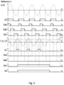
- the example illustrates the time course of all signals when the reference phase is L1 and the AC input signal I_k is also derived from L1 (I_k_L1).
- the input I_k_L1 is represented by the signal S1 as "1" for three periods (the amplitude exceeds the amplitude threshold A) and for another two periods as "0" (the amplitude is smaller than the amplitude threshold A).
- the signal S4a from the signal S1 - controlled by the falling clock edge of the clock signal S3a - accepted as "1" or "0” accordingly, S4b and S4c remain “0".
- S4 corresponds to the signal S4a and reflects the state of the input I_k_L1 with the corresponding delay (T/4).
- FIG 5 shows the time course of all signals for the case that the AC input signal I_k is derived from L3 (I_k_L3).
- the input I_k_L3 is represented by the signal S1 as "1" for three periods (the amplitude exceeds the amplitude threshold A) and for another two periods as “0" (the amplitude is smaller than the amplitude threshold A).
- the signal S4c from the signal S1—controlled by the falling clock edge of the clock signal S3c— is taken over as “1” or “0”, S4a and S4b remain “0”.
- the method enables the corresponding input signals I_k_L1, I_k_L2, I_k_L3 to be recorded within a period T, e.g. at 50Hz after 20ms at the latest.
- FIGS 1A and 1B marked elements (timers 12a, 12b, 12c, flip-flops 14a, 14b 14c, OR gate 15) implemented in a microcontroller 16.
- the input signals S1 (one or more) are switched on as normal inputs.
- the zero crossing signal S2 is switched on at an interrupt input.
- the OR gate 15 can be implemented as an OR function in software by the microcontroller 16 .
- FIG. 6 shows in principle how processing can be carried out in software.
- an interrupt routine of the microcontroller 16 triggered by an interrupt (referred to here as an interruption) of the second output signal S2
- a first timer for realizing the first timer 12a is started with the value T/4, which at the end (after its expiration) generates another interrupt.
- the first output signals S1 are read and the first status signals S4a are correspondingly stored in the memory.
- the first timer for realizing the second timer 12b is restarted with the value T/3.
- the first timer thus implements the first, second and third timer 12a, 12b, 12c.
- a timer can also be called a timer.
- the interrupt can also be called an interruption.
- first, second and third timer 12a, 12b, 12c can be implemented by a first, a second and a third timer or clocks which are started in a chained manner.
- the delay values are also T/4, T/3 and T/3.
- the first, second and third timer 12a, 12b, 12c can be realized by a first, a second and a third timer or timer, which are started in parallel after the interruption by the second output signal S2.
- the delay value of the first timer is then T/4, the second timer T • 7/12 and the third timer T • 11/12.
- At least one further AC input signal I_k' can be supplied to the circuit arrangement.
- the other AC input signal I_k' can also be tapped off at one of the phases La, Lb or LC.
- the circuit arrangement can therefore comprise at least one further comparator and three further flip-flops connected downstream.
- the signals of the zero crossing detector 10 and the timers 12a, 12b, 12c are suitable for monitoring whether the amplitude of the further AC input signal I_k' is above the amplitude threshold value A.
- a number of n AC input signals, which can be tapped at any one of the three different phases L1, L2 or L3, is fed to the circuit arrangement and recorded. n can be equal to 1 or 2 or greater than 2.
Landscapes
- Engineering & Computer Science (AREA)
- Power Engineering (AREA)
- Physics & Mathematics (AREA)
- General Physics & Mathematics (AREA)
- Automation & Control Theory (AREA)
- Manipulation Of Pulses (AREA)
- Measurement Of Current Or Voltage (AREA)
Applications Claiming Priority (2)
| Application Number | Priority Date | Filing Date | Title |
|---|---|---|---|
| DE102017116534.7A DE102017116534A1 (de) | 2017-07-21 | 2017-07-21 | Schaltungsanordnung und Verfahren zur Überwachung wechselspannungsförmiger Signale |
| PCT/EP2018/068381 WO2019015998A1 (de) | 2017-07-21 | 2018-07-06 | Schaltungsanordnung und verfahren zur überwachung wechselspannungsförmiger signale |
Publications (2)
| Publication Number | Publication Date |
|---|---|
| EP3655785A1 EP3655785A1 (de) | 2020-05-27 |
| EP3655785B1 true EP3655785B1 (de) | 2023-05-31 |
Family
ID=62837941
Family Applications (1)
| Application Number | Title | Priority Date | Filing Date |
|---|---|---|---|
| EP18737616.5A Active EP3655785B1 (de) | 2017-07-21 | 2018-07-06 | Schaltungsanordnung und verfahren zur überwachung wechselspannungsförmiger signale |
Country Status (6)
| Country | Link |
|---|---|
| US (1) | US11402411B2 (pl) |
| EP (1) | EP3655785B1 (pl) |
| CN (1) | CN111095001B (pl) |
| DE (1) | DE102017116534A1 (pl) |
| PL (1) | PL3655785T3 (pl) |
| WO (1) | WO2019015998A1 (pl) |
Families Citing this family (3)
| Publication number | Priority date | Publication date | Assignee | Title |
|---|---|---|---|---|
| DE102019107641A1 (de) * | 2019-03-25 | 2020-10-01 | Eaton Intelligent Power Limited | Schaltungsanordnung und Verfahren zur Überwachung eines wechselspannungsförmigen Signals |
| WO2021070788A1 (ja) * | 2019-10-08 | 2021-04-15 | Agc株式会社 | 撥水撥油層付き物品 |
| CN113485181B (zh) * | 2021-06-30 | 2022-07-08 | 浙江中控技术股份有限公司 | 一种基于故障检测的通信总线控制系统 |
Family Cites Families (17)
| Publication number | Priority date | Publication date | Assignee | Title |
|---|---|---|---|---|
| US3611162A (en) * | 1970-07-09 | 1971-10-05 | Yokogawa Electric Works Ltd | Apparatus for detecting abnormal conditions of ac sources |
| US3836854A (en) * | 1973-07-02 | 1974-09-17 | Lorain Prod Corp | Alarm circuit for monitoring the amplitude of a-c voltages |
| US4594517A (en) * | 1984-04-30 | 1986-06-10 | Rca Corporation | Power down sensor |
| JPH04230868A (ja) * | 1990-05-08 | 1992-08-19 | Toshiba Corp | 交流データ検出装置 |
| EP0935758B1 (de) | 1997-11-04 | 2001-05-23 | Moeller GmbH | Verfahren und schaltungsanordnung zur überwachung eines definierten amplitudenschwellenwertes wechselspannungsförmiger signale |
| DE19748633A1 (de) * | 1997-11-04 | 1999-05-06 | Kloeckner Moeller Gmbh | Verfahren und Schaltungsanordnung zur Überwachung eines definierten Amplitudenschwellenwertes wechselspannungsförmiger Eingangssignale |
| US6072317A (en) * | 1998-03-27 | 2000-06-06 | Eaton Corporation | Plug-in multifunction tester for AC electrical distribution system |
| KR100606144B1 (ko) * | 2002-03-06 | 2006-08-01 | 산켄덴키 가부시키가이샤 | 교류신호의 레벨검출회로 |
| JP2007093499A (ja) * | 2005-09-30 | 2007-04-12 | Japan Aviation Electronics Industry Ltd | フラックスゲート型磁気センサ |
| US7649360B2 (en) * | 2008-01-18 | 2010-01-19 | Gm Global Technology Operations, Inc. | Apparatus and systems for common mode voltage-based AC fault detection, verification and/or identification |
| US9143141B2 (en) * | 2009-10-05 | 2015-09-22 | Siemens Industry, Inc. | Apparatus and methods for power quality measurement |
| US8553439B2 (en) * | 2010-02-09 | 2013-10-08 | Power Integrations, Inc. | Method and apparatus for determining zero-crossing of an AC input voltage to a power supply |
| WO2012048349A1 (en) * | 2010-10-08 | 2012-04-12 | Energy Focus, Inc. | Switching power supply circuit with reduced total harmonic distortion |
| CN102447381B (zh) * | 2010-10-11 | 2014-07-16 | 辉芒微电子(深圳)有限公司 | 功率因数校正装置、在该装置中使用的控制器和thd衰减器 |
| US9121877B2 (en) * | 2011-09-19 | 2015-09-01 | Honeywell International Inc. | System and method for wireless remote display for high voltage line meter |
| CN204177858U (zh) * | 2014-11-12 | 2015-02-25 | 福建龙净环保股份有限公司 | 一种三相电检测电路 |
| US10107841B2 (en) * | 2015-07-24 | 2018-10-23 | Texas Instruments Incorporated | Methods and apparatus for peak-voltage measurement of AC signals |
-
2017
- 2017-07-21 DE DE102017116534.7A patent/DE102017116534A1/de not_active Withdrawn
-
2018
- 2018-07-06 WO PCT/EP2018/068381 patent/WO2019015998A1/de not_active Ceased
- 2018-07-06 CN CN201880059334.2A patent/CN111095001B/zh active Active
- 2018-07-06 US US16/631,845 patent/US11402411B2/en active Active
- 2018-07-06 PL PL18737616.5T patent/PL3655785T3/pl unknown
- 2018-07-06 EP EP18737616.5A patent/EP3655785B1/de active Active
Also Published As
| Publication number | Publication date |
|---|---|
| DE102017116534A1 (de) | 2019-01-24 |
| US20200191838A1 (en) | 2020-06-18 |
| EP3655785A1 (de) | 2020-05-27 |
| US11402411B2 (en) | 2022-08-02 |
| CN111095001B (zh) | 2022-10-14 |
| CN111095001A (zh) | 2020-05-01 |
| WO2019015998A1 (de) | 2019-01-24 |
| PL3655785T3 (pl) | 2023-09-11 |
Similar Documents
| Publication | Publication Date | Title |
|---|---|---|
| DE4131128C1 (pl) | ||
| EP3655785B1 (de) | Schaltungsanordnung und verfahren zur überwachung wechselspannungsförmiger signale | |
| EP3942307B1 (de) | Vorrichtung zur analyse von strömen in einem elektrischen verbraucher und verbraucher mit einer derartigen vorrichtung | |
| EP2920883A1 (de) | Verfahren und vorrichtung zum einschalten oder abschalten eines elektronischen bauelements | |
| WO2014060330A1 (de) | Verfahren und einrichtung zur messung eines stroms durch einen schalter | |
| EP3711160B1 (de) | Schaltungsanordnung und verfahren zur überwachung sinusförmiger wechselspannungssignale | |
| EP2622358B1 (de) | Verfahren und anordnung zur frequenzbestimmung | |
| EP0935758B1 (de) | Verfahren und schaltungsanordnung zur überwachung eines definierten amplitudenschwellenwertes wechselspannungsförmiger signale | |
| EP3948311B1 (de) | Schaltungsanordnung und verfahren zur überwachung eines wechselspannungsförmigen signals | |
| EP1900088B1 (de) | Schaltungsanordnung zur ermittlung von nulldurchgängen einer wechselspannung | |
| EP1340988A2 (de) | Verfahren und Vorrichtung zur Messung der Impedanz eines elektrischen Energieversorgungsnetzes | |
| EP3375087B1 (de) | Schnittstelle | |
| EP3186876B1 (de) | Leistungsfaktorkorrektur mit erfassung von nulldurchgängen | |
| EP1894284B1 (de) | Verfahren und anordnung zur überwachung von signalen | |
| DE3527619C1 (de) | Selbstprüfender Näherungsschalter | |
| DE102016206439A1 (de) | Schnittstelleneinheit, System und Verfahren zum Übertragen von Daten über eine Energieversorgungsleitung | |
| DE2554223A1 (de) | Einrichtung an einem wechselrichter | |
| DE1900260C3 (de) | Ortsveränderungsmeßvorrichtung | |
| DE102017108912B3 (de) | Verfahren zur Auswertung eines Messsignals eines induktiven Messsensors sowie ein Längenmesssystem | |
| EP4053569A1 (de) | Verfahren und system zum auswerten einer eingangsspannung einer stromversorgung | |
| DE2822562C2 (de) | Anordnung zur Erfassung von Störungen bei Stromrichtern | |
| DE1516242C3 (de) | Phasenvergleicheinrichtung | |
| DE2917804C2 (de) | Detektorschaltung | |
| DE102015216848A1 (de) | Verfahren zum Betreiben eines piezoelektrischen Elements, Vorrichtung zur Durchführung des Verfahrens, Steuergerät-Programm und Steuergerät-Programmprodukt | |
| DE19748633A1 (de) | Verfahren und Schaltungsanordnung zur Überwachung eines definierten Amplitudenschwellenwertes wechselspannungsförmiger Eingangssignale |
Legal Events
| Date | Code | Title | Description |
|---|---|---|---|
| STAA | Information on the status of an ep patent application or granted ep patent |
Free format text: STATUS: UNKNOWN |
|
| STAA | Information on the status of an ep patent application or granted ep patent |
Free format text: STATUS: THE INTERNATIONAL PUBLICATION HAS BEEN MADE |
|
| PUAI | Public reference made under article 153(3) epc to a published international application that has entered the european phase |
Free format text: ORIGINAL CODE: 0009012 |
|
| STAA | Information on the status of an ep patent application or granted ep patent |
Free format text: STATUS: REQUEST FOR EXAMINATION WAS MADE |
|
| 17P | Request for examination filed |
Effective date: 20200113 |
|
| AK | Designated contracting states |
Kind code of ref document: A1 Designated state(s): AL AT BE BG CH CY CZ DE DK EE ES FI FR GB GR HR HU IE IS IT LI LT LU LV MC MK MT NL NO PL PT RO RS SE SI SK SM TR |
|
| AX | Request for extension of the european patent |
Extension state: BA ME |
|
| DAV | Request for validation of the european patent (deleted) | ||
| DAX | Request for extension of the european patent (deleted) | ||
| GRAP | Despatch of communication of intention to grant a patent |
Free format text: ORIGINAL CODE: EPIDOSNIGR1 |
|
| STAA | Information on the status of an ep patent application or granted ep patent |
Free format text: STATUS: GRANT OF PATENT IS INTENDED |
|
| INTG | Intention to grant announced |
Effective date: 20221115 |
|
| GRAS | Grant fee paid |
Free format text: ORIGINAL CODE: EPIDOSNIGR3 |
|
| GRAA | (expected) grant |
Free format text: ORIGINAL CODE: 0009210 |
|
| STAA | Information on the status of an ep patent application or granted ep patent |
Free format text: STATUS: THE PATENT HAS BEEN GRANTED |
|
| AK | Designated contracting states |
Kind code of ref document: B1 Designated state(s): AL AT BE BG CH CY CZ DE DK EE ES FI FR GB GR HR HU IE IS IT LI LT LU LV MC MK MT NL NO PL PT RO RS SE SI SK SM TR |
|
| REG | Reference to a national code |
Ref country code: GB Ref legal event code: FG4D Free format text: NOT ENGLISH Ref country code: CH Ref legal event code: EP |
|
| REG | Reference to a national code |
Ref country code: DE Ref legal event code: R096 Ref document number: 502018012217 Country of ref document: DE |
|
| REG | Reference to a national code |
Ref country code: AT Ref legal event code: REF Ref document number: 1571222 Country of ref document: AT Kind code of ref document: T Effective date: 20230615 |
|
| REG | Reference to a national code |
Ref country code: IE Ref legal event code: FG4D Free format text: LANGUAGE OF EP DOCUMENT: GERMAN |
|
| P01 | Opt-out of the competence of the unified patent court (upc) registered |
Effective date: 20230521 |
|
| REG | Reference to a national code |
Ref country code: NL Ref legal event code: FP |
|
| REG | Reference to a national code |
Ref country code: LT Ref legal event code: MG9D |
|
| PG25 | Lapsed in a contracting state [announced via postgrant information from national office to epo] |
Ref country code: SE Free format text: LAPSE BECAUSE OF FAILURE TO SUBMIT A TRANSLATION OF THE DESCRIPTION OR TO PAY THE FEE WITHIN THE PRESCRIBED TIME-LIMIT Effective date: 20230531 Ref country code: NO Free format text: LAPSE BECAUSE OF FAILURE TO SUBMIT A TRANSLATION OF THE DESCRIPTION OR TO PAY THE FEE WITHIN THE PRESCRIBED TIME-LIMIT Effective date: 20230831 Ref country code: ES Free format text: LAPSE BECAUSE OF FAILURE TO SUBMIT A TRANSLATION OF THE DESCRIPTION OR TO PAY THE FEE WITHIN THE PRESCRIBED TIME-LIMIT Effective date: 20230531 |
|
| PG25 | Lapsed in a contracting state [announced via postgrant information from national office to epo] |
Ref country code: RS Free format text: LAPSE BECAUSE OF FAILURE TO SUBMIT A TRANSLATION OF THE DESCRIPTION OR TO PAY THE FEE WITHIN THE PRESCRIBED TIME-LIMIT Effective date: 20230531 Ref country code: LV Free format text: LAPSE BECAUSE OF FAILURE TO SUBMIT A TRANSLATION OF THE DESCRIPTION OR TO PAY THE FEE WITHIN THE PRESCRIBED TIME-LIMIT Effective date: 20230531 Ref country code: LT Free format text: LAPSE BECAUSE OF FAILURE TO SUBMIT A TRANSLATION OF THE DESCRIPTION OR TO PAY THE FEE WITHIN THE PRESCRIBED TIME-LIMIT Effective date: 20230531 Ref country code: IS Free format text: LAPSE BECAUSE OF FAILURE TO SUBMIT A TRANSLATION OF THE DESCRIPTION OR TO PAY THE FEE WITHIN THE PRESCRIBED TIME-LIMIT Effective date: 20230930 Ref country code: HR Free format text: LAPSE BECAUSE OF FAILURE TO SUBMIT A TRANSLATION OF THE DESCRIPTION OR TO PAY THE FEE WITHIN THE PRESCRIBED TIME-LIMIT Effective date: 20230531 Ref country code: GR Free format text: LAPSE BECAUSE OF FAILURE TO SUBMIT A TRANSLATION OF THE DESCRIPTION OR TO PAY THE FEE WITHIN THE PRESCRIBED TIME-LIMIT Effective date: 20230901 |
|
| PG25 | Lapsed in a contracting state [announced via postgrant information from national office to epo] |
Ref country code: FI Free format text: LAPSE BECAUSE OF FAILURE TO SUBMIT A TRANSLATION OF THE DESCRIPTION OR TO PAY THE FEE WITHIN THE PRESCRIBED TIME-LIMIT Effective date: 20230531 |
|
| PG25 | Lapsed in a contracting state [announced via postgrant information from national office to epo] |
Ref country code: SK Free format text: LAPSE BECAUSE OF FAILURE TO SUBMIT A TRANSLATION OF THE DESCRIPTION OR TO PAY THE FEE WITHIN THE PRESCRIBED TIME-LIMIT Effective date: 20230531 |
|
| PG25 | Lapsed in a contracting state [announced via postgrant information from national office to epo] |
Ref country code: SM Free format text: LAPSE BECAUSE OF FAILURE TO SUBMIT A TRANSLATION OF THE DESCRIPTION OR TO PAY THE FEE WITHIN THE PRESCRIBED TIME-LIMIT Effective date: 20230531 Ref country code: SK Free format text: LAPSE BECAUSE OF FAILURE TO SUBMIT A TRANSLATION OF THE DESCRIPTION OR TO PAY THE FEE WITHIN THE PRESCRIBED TIME-LIMIT Effective date: 20230531 Ref country code: RO Free format text: LAPSE BECAUSE OF FAILURE TO SUBMIT A TRANSLATION OF THE DESCRIPTION OR TO PAY THE FEE WITHIN THE PRESCRIBED TIME-LIMIT Effective date: 20230531 Ref country code: PT Free format text: LAPSE BECAUSE OF FAILURE TO SUBMIT A TRANSLATION OF THE DESCRIPTION OR TO PAY THE FEE WITHIN THE PRESCRIBED TIME-LIMIT Effective date: 20231002 Ref country code: EE Free format text: LAPSE BECAUSE OF FAILURE TO SUBMIT A TRANSLATION OF THE DESCRIPTION OR TO PAY THE FEE WITHIN THE PRESCRIBED TIME-LIMIT Effective date: 20230531 Ref country code: DK Free format text: LAPSE BECAUSE OF FAILURE TO SUBMIT A TRANSLATION OF THE DESCRIPTION OR TO PAY THE FEE WITHIN THE PRESCRIBED TIME-LIMIT Effective date: 20230531 Ref country code: CZ Free format text: LAPSE BECAUSE OF FAILURE TO SUBMIT A TRANSLATION OF THE DESCRIPTION OR TO PAY THE FEE WITHIN THE PRESCRIBED TIME-LIMIT Effective date: 20230531 |
|
| PG25 | Lapsed in a contracting state [announced via postgrant information from national office to epo] |
Ref country code: MC Free format text: LAPSE BECAUSE OF FAILURE TO SUBMIT A TRANSLATION OF THE DESCRIPTION OR TO PAY THE FEE WITHIN THE PRESCRIBED TIME-LIMIT Effective date: 20230531 |
|
| PG25 | Lapsed in a contracting state [announced via postgrant information from national office to epo] |
Ref country code: MC Free format text: LAPSE BECAUSE OF FAILURE TO SUBMIT A TRANSLATION OF THE DESCRIPTION OR TO PAY THE FEE WITHIN THE PRESCRIBED TIME-LIMIT Effective date: 20230531 |
|
| REG | Reference to a national code |
Ref country code: DE Ref legal event code: R097 Ref document number: 502018012217 Country of ref document: DE |
|
| REG | Reference to a national code |
Ref country code: BE Ref legal event code: MM Effective date: 20230731 |
|
| PG25 | Lapsed in a contracting state [announced via postgrant information from national office to epo] |
Ref country code: LU Free format text: LAPSE BECAUSE OF NON-PAYMENT OF DUE FEES Effective date: 20230706 |
|
| PG25 | Lapsed in a contracting state [announced via postgrant information from national office to epo] |
Ref country code: LU Free format text: LAPSE BECAUSE OF NON-PAYMENT OF DUE FEES Effective date: 20230706 |
|
| PLBE | No opposition filed within time limit |
Free format text: ORIGINAL CODE: 0009261 |
|
| STAA | Information on the status of an ep patent application or granted ep patent |
Free format text: STATUS: NO OPPOSITION FILED WITHIN TIME LIMIT |
|
| REG | Reference to a national code |
Ref country code: IE Ref legal event code: MM4A |
|
| PG25 | Lapsed in a contracting state [announced via postgrant information from national office to epo] |
Ref country code: SI Free format text: LAPSE BECAUSE OF FAILURE TO SUBMIT A TRANSLATION OF THE DESCRIPTION OR TO PAY THE FEE WITHIN THE PRESCRIBED TIME-LIMIT Effective date: 20230531 |
|
| 26N | No opposition filed |
Effective date: 20240301 |
|
| PG25 | Lapsed in a contracting state [announced via postgrant information from national office to epo] |
Ref country code: SI Free format text: LAPSE BECAUSE OF FAILURE TO SUBMIT A TRANSLATION OF THE DESCRIPTION OR TO PAY THE FEE WITHIN THE PRESCRIBED TIME-LIMIT Effective date: 20230531 Ref country code: BE Free format text: LAPSE BECAUSE OF NON-PAYMENT OF DUE FEES Effective date: 20230731 |
|
| PG25 | Lapsed in a contracting state [announced via postgrant information from national office to epo] |
Ref country code: IE Free format text: LAPSE BECAUSE OF NON-PAYMENT OF DUE FEES Effective date: 20230706 |
|
| PG25 | Lapsed in a contracting state [announced via postgrant information from national office to epo] |
Ref country code: IE Free format text: LAPSE BECAUSE OF NON-PAYMENT OF DUE FEES Effective date: 20230706 |
|
| REG | Reference to a national code |
Ref country code: AT Ref legal event code: MM01 Ref document number: 1571222 Country of ref document: AT Kind code of ref document: T Effective date: 20230706 |
|
| PG25 | Lapsed in a contracting state [announced via postgrant information from national office to epo] |
Ref country code: AT Free format text: LAPSE BECAUSE OF NON-PAYMENT OF DUE FEES Effective date: 20230706 |
|
| PG25 | Lapsed in a contracting state [announced via postgrant information from national office to epo] |
Ref country code: AT Free format text: LAPSE BECAUSE OF NON-PAYMENT OF DUE FEES Effective date: 20230706 |
|
| PG25 | Lapsed in a contracting state [announced via postgrant information from national office to epo] |
Ref country code: BG Free format text: LAPSE BECAUSE OF FAILURE TO SUBMIT A TRANSLATION OF THE DESCRIPTION OR TO PAY THE FEE WITHIN THE PRESCRIBED TIME-LIMIT Effective date: 20230531 |
|
| PG25 | Lapsed in a contracting state [announced via postgrant information from national office to epo] |
Ref country code: BG Free format text: LAPSE BECAUSE OF FAILURE TO SUBMIT A TRANSLATION OF THE DESCRIPTION OR TO PAY THE FEE WITHIN THE PRESCRIBED TIME-LIMIT Effective date: 20230531 |
|
| PGFP | Annual fee paid to national office [announced via postgrant information from national office to epo] |
Ref country code: PL Payment date: 20250625 Year of fee payment: 8 |
|
| PGFP | Annual fee paid to national office [announced via postgrant information from national office to epo] |
Ref country code: GB Payment date: 20250619 Year of fee payment: 8 |
|
| PGFP | Annual fee paid to national office [announced via postgrant information from national office to epo] |
Ref country code: NL Payment date: 20250620 Year of fee payment: 8 |
|
| PGFP | Annual fee paid to national office [announced via postgrant information from national office to epo] |
Ref country code: FR Payment date: 20250620 Year of fee payment: 8 |
|
| PG25 | Lapsed in a contracting state [announced via postgrant information from national office to epo] |
Ref country code: CY Free format text: LAPSE BECAUSE OF FAILURE TO SUBMIT A TRANSLATION OF THE DESCRIPTION OR TO PAY THE FEE WITHIN THE PRESCRIBED TIME-LIMIT; INVALID AB INITIO Effective date: 20180706 |
|
| PG25 | Lapsed in a contracting state [announced via postgrant information from national office to epo] |
Ref country code: HU Free format text: LAPSE BECAUSE OF FAILURE TO SUBMIT A TRANSLATION OF THE DESCRIPTION OR TO PAY THE FEE WITHIN THE PRESCRIBED TIME-LIMIT; INVALID AB INITIO Effective date: 20180706 |
|
| PGFP | Annual fee paid to national office [announced via postgrant information from national office to epo] |
Ref country code: DE Payment date: 20250620 Year of fee payment: 8 |
|
| PGFP | Annual fee paid to national office [announced via postgrant information from national office to epo] |
Ref country code: IT Payment date: 20250619 Year of fee payment: 8 |
|
| PGFP | Annual fee paid to national office [announced via postgrant information from national office to epo] |
Ref country code: CH Payment date: 20250801 Year of fee payment: 8 |
|
| PG25 | Lapsed in a contracting state [announced via postgrant information from national office to epo] |
Ref country code: TR Free format text: LAPSE BECAUSE OF FAILURE TO SUBMIT A TRANSLATION OF THE DESCRIPTION OR TO PAY THE FEE WITHIN THE PRESCRIBED TIME-LIMIT Effective date: 20230531 |