EP3657665A1 - Spannungskonditionierer und steuergerät für wechselstromleitung - Google Patents
Spannungskonditionierer und steuergerät für wechselstromleitung Download PDFInfo
- Publication number
- EP3657665A1 EP3657665A1 EP20151669.7A EP20151669A EP3657665A1 EP 3657665 A1 EP3657665 A1 EP 3657665A1 EP 20151669 A EP20151669 A EP 20151669A EP 3657665 A1 EP3657665 A1 EP 3657665A1
- Authority
- EP
- European Patent Office
- Prior art keywords
- power
- voltage
- electrode
- load
- line
- Prior art date
- Legal status (The legal status is an assumption and is not a legal conclusion. Google has not performed a legal analysis and makes no representation as to the accuracy of the status listed.)
- Withdrawn
Links
Images


Classifications
-
- H—ELECTRICITY
- H02—GENERATION; CONVERSION OR DISTRIBUTION OF ELECTRIC POWER
- H02P—CONTROL OR REGULATION OF ELECTRIC MOTORS, ELECTRIC GENERATORS OR DYNAMO-ELECTRIC CONVERTERS; CONTROLLING TRANSFORMERS, REACTORS OR CHOKE COILS
- H02P1/00—Arrangements for starting electric motors or dynamo-electric converters
- H02P1/16—Arrangements for starting electric motors or dynamo-electric converters for starting dynamo-electric motors or dynamo-electric converters
- H02P1/42—Arrangements for starting electric motors or dynamo-electric converters for starting dynamo-electric motors or dynamo-electric converters for starting an individual single-phase induction motor
-
- H—ELECTRICITY
- H02—GENERATION; CONVERSION OR DISTRIBUTION OF ELECTRIC POWER
- H02J—ELECTRIC POWER NETWORKS; CIRCUIT ARRANGEMENTS OR SYSTEMS FOR SUPPLYING OR DISTRIBUTING ELECTRIC POWER; SYSTEMS FOR STORING ELECTRIC ENERGY
- H02J3/00—Circuit arrangements for AC mains or AC distribution networks
- H02J3/38—Arrangements for feeding a single network from two or more generators or sources in parallel; Arrangements for feeding already energised networks from additional generators or sources in parallel
- H02J3/381—Dispersed generators
-
- H—ELECTRICITY
- H02—GENERATION; CONVERSION OR DISTRIBUTION OF ELECTRIC POWER
- H02M—APPARATUS FOR CONVERSION BETWEEN AC AND AC, BETWEEN AC AND DC, OR BETWEEN DC AND DC, AND FOR USE WITH MAINS OR SIMILAR POWER SUPPLY SYSTEMS; CONVERSION OF DC OR AC INPUT POWER INTO SURGE OUTPUT POWER; CONTROL OR REGULATION THEREOF
- H02M5/00—Conversion of AC power input into AC power output, e.g. for change of voltage, for change of frequency, for change of number of phases
- H02M5/02—Conversion of AC power input into AC power output, e.g. for change of voltage, for change of frequency, for change of number of phases without intermediate conversion into DC
- H02M5/04—Conversion of AC power input into AC power output, e.g. for change of voltage, for change of frequency, for change of number of phases without intermediate conversion into DC by static converters
- H02M5/22—Conversion of AC power input into AC power output, e.g. for change of voltage, for change of frequency, for change of number of phases without intermediate conversion into DC by static converters using discharge tubes with control electrode or semiconductor devices with control electrode
- H02M5/275—Conversion of AC power input into AC power output, e.g. for change of voltage, for change of frequency, for change of number of phases without intermediate conversion into DC by static converters using discharge tubes with control electrode or semiconductor devices with control electrode using devices of a triode or transistor type requiring continuous application of a control signal
- H02M5/293—Conversion of AC power input into AC power output, e.g. for change of voltage, for change of frequency, for change of number of phases without intermediate conversion into DC by static converters using discharge tubes with control electrode or semiconductor devices with control electrode using devices of a triode or transistor type requiring continuous application of a control signal using semiconductor devices only
-
- H—ELECTRICITY
- H02—GENERATION; CONVERSION OR DISTRIBUTION OF ELECTRIC POWER
- H02J—ELECTRIC POWER NETWORKS; CIRCUIT ARRANGEMENTS OR SYSTEMS FOR SUPPLYING OR DISTRIBUTING ELECTRIC POWER; SYSTEMS FOR STORING ELECTRIC ENERGY
- H02J2101/00—Supply or distribution of decentralised, dispersed or local electric power generation
- H02J2101/20—Dispersed power generation using renewable energy sources
- H02J2101/22—Solar energy
- H02J2101/24—Photovoltaics
-
- Y—GENERAL TAGGING OF NEW TECHNOLOGICAL DEVELOPMENTS; GENERAL TAGGING OF CROSS-SECTIONAL TECHNOLOGIES SPANNING OVER SEVERAL SECTIONS OF THE IPC; TECHNICAL SUBJECTS COVERED BY FORMER USPC CROSS-REFERENCE ART COLLECTIONS [XRACs] AND DIGESTS
- Y02—TECHNOLOGIES OR APPLICATIONS FOR MITIGATION OR ADAPTATION AGAINST CLIMATE CHANGE
- Y02E—REDUCTION OF GREENHOUSE GAS [GHG] EMISSIONS, RELATED TO ENERGY GENERATION, TRANSMISSION OR DISTRIBUTION
- Y02E10/00—Energy generation through renewable energy sources
- Y02E10/50—Photovoltaic [PV] energy
- Y02E10/56—Power conversion systems, e.g. maximum power point trackers
Definitions
- the present invention relates to devices that regulate, condition and control AC power that is provided to an AC load, such as an induction motor.
- the invention is more specifically directed to an AC power conditioning device that can adjust the wave shape and voltage level of AC power applied to an AC load, as well as power factor and frequency, to compensate for deterioration in quality of the AC line power.
- the power conditioning device of this invention can be used with motors from fractional horsepower to several horsepower or above, and where the torsional load on the motor may vary depending upon external factors, and in situations where the quality of the line power may drop, i.e., from a nominal 117 VAC (in North America) to below 100 VAC.
- the device may be employed for controlling the power factor for an AC or inductive load that may vary during use, such as a single-phase AC induction motor, which may be used to drive a compressor in a HVAC application or in a refrigerator.
- the available motor torque can depend on the condition or quality of the AC line power.
- the output torque is proportional to the square of the input voltage.
- the quality of the AC line power can vary enormously, with changes in line voltage and in line frequency.
- a drop in line voltage from 117 VAC to 100 VAC (a drop of about 14.5%) results in a reduction in torque of about 27 %.
- the motor designer is forced to over-design the motor in order to satisfy load requirements over an expected range of input conditions.
- the motor armature which is basically an inductive load, may have to face an unfavorable power factor, which means that the actual applied voltage, i.e., the real component of the complex AC voltage, may become unacceptably low. Consequently, it is desirable to adjust the RMS value of the line voltage so that the motor will operate optimally, even under adverse line conditions.
- VFD variable frequency drive
- PWM pulse-width modulation
- phase detection power factor controller circuit which addresses some of these issues, is discussed in Nola U.S. Pat. 4,459,528 .
- an active power factor converter is discussed, which reduces the effective applied power by use of a thyristor (triac) and turning the thyristor on and off at various phase angles so as to change the shape of the applied power wave and optimize the phase angle or power factor.
- Another power factor controller is discussed in Bach Published Application No. US 2003/0122433 .
- the device described there is an active power factor controller with power factor correction and also with a soft-start feature for applying a gradually increasing voltage to the AC load at turn on. These are accomplished by switching the applied power to regulate the amount of the AC input power that passes to the load. These can reduce effective applied voltage but do not boost the power (i.e., voltage) applied to the load.
- Power factor (phase angle) correction is a problem for both consumers of AC power and commercial providers.
- the common practice is to place one or more capacitors in parallel to the load (in the case of an inductive device such as a motor armature).
- the size of the capacitor has to be selected to match the motor impedance, which can change with line and load conditions. This means that a number of capacitors have to be placed in parallel and switched in or out of circuit as conditions change.
- This technique requires high capacity AC devices, which are bulky and pricey.
- brownout protection i.e., to protect the AC induction motor from burn out in low line voltage situations
- a freezer system may be used for storage of a frozen food product, e.g., frozen meat, ice cream, or another food product.
- a safe threshold e.g., reduced from 120 volts RMS to below 95 volts RMS
- the meat may begin to spoil, or the ice cream may melt. It would be more desirable to continue to operate the refrigeration system during brownouts, i.e., modifying the AC power wave so that it is sufficient to run the equipment, even if at a partial speed. However, that has not been possible with existing power control circuits.
- an AC load such as a motor armature
- a further object is to provide an AC power conditioning device having features or capabilities for soft start, hard start, voltage regulation of ⁇ 30% or better, and power factor correction.
- other objects include source and/or load impedance matching to achieve maximum power transfer; capability for metering of volts, amperes, power, power factor, and watt-hours to achieve economy of operation; facilitation of programmable energy management system; as well as motor control capabilities to correct or adjust for phase loss, phase rotation or phase correction (in a three-phase system); correction of voltage imbalance; under-voltage and over-voltage protection; programmable overload protection; and communication with power provider, e.g. for off-peak pricing differentials.
- further objects include motor speed control through variable voltage and motor speed control through variable frequency (line frequency and applied power frequency need not be the same).
- another object is to provide inverter capabilities for use with a DC power source, including tying to a solar or other power source (to substitute for a so-called grid tie inverter system) and to provide a "green energy system.”
- Still further objects are arc interruption and ground fault interruption capabilities.
- power factor can be corrected with the use of a capacitance to increase or reduce the applied motor voltage, without the drastic chopping of the power wave, and without the associated RF radiation that is characteristic of current systems.
- Command signals are applied to respective switching components, which may be IGBTs, MOSFETs, power transistors or the like. Other possible switching components may be SCRs, Triacs, or Silicon Bilateral Switches.
- the command signals may come from logic components (e.g., op-amps, differential amps, etc.) or a microprocessor, and these may be communicated directly or indirectly (e.g., with an opto-isolator) to the associated power switching components. In some components, a gate may not be required.
- an in-line voltage regulation circuit device is capable of responding to changes in quality of a single-phase AC input line power that is to be applied, at an adjusted AC voltage level, to a two-terminal single-phase induction motor or other AC load device.
- the voltage regulation circuit has a provision for connecting to a source of such single-phase AC line power, having a first AC power conductor and a second AC power conductor.
- a two-input line voltage regulator has first and second AC power terminals, the first AC power terminal being connected to the first AC power conductor and the second AC power terminal being connected to a first AC power terminal of the load, with the second AC terminal of the load being connected to the second AC power conductor.
- An associated control signal generator can have one or more sensor inputs coupled with the AC power source, and has provisions to detect the AC voltage level of the AC input line power and to detect zero crossings and polarity of the AC line power, and has outputs to provide first and second command signals to the line voltage regulator. These command signals are employed for the timed gating of power switching components.
- the two-line voltage regulator favorably includes first and second power capacitors, each having a first electrode and a second electrode, with the first electrode of the first power capacitor and the second electrode of the second power capacitor each being connected to the first AC power terminal of the voltage regulator.
- First and second electronic switching devices each have a first power electrode, a second power electrode, and a gate, with the first power electrode of the first switching device and the second power electrode of the second switching device each being connected to the second AC power terminal of the voltage regulator.
- the second electrode of the first power capacitor is connected to the second power electrode of the first switching device and the first electrode of the second power capacitor is connected to the first power electrode of the second switching device.
- the first and second outputs of the control signal generator are coupled to the gates of the first and second electronic switching devices, respectively. This may be a transformer coupling, an optical coupling, or other suitable means of gating the devices.
- Power diodes are favorably connected in parallel with first and second electronic switching devices.
- the power diodes can each have an anode connected with the first power electrode of the associated switching device and a cathode connected with the second power electrode of the associated switching device.
- the power capacitors are considered to be in series with the load, which most frequently is an inductive load, i.e., a motor winding. That is, one capacitor is in series circuit relation with the load (motor winding) during the positive half cycle and the other capacitor during the negative half cycle. This arrangement tends to correct the phase lag inherent with the motor and improves the circuit power factor. Because the switching devices (e.g., transistors) associated with the regulation circuit control the charging and timed discharging of these capacitors, the amount of power angle correction will vary automatically with changes in load to optimize power factor correction at all times during operation.
- the switching devices e.g., transistors
- the illustrated embodiments are employed in a single phase system, but a multiple of these arrangements can be employed with the respective phases of poly-phase (e.g., three-phase) AC power systems. In the case of a delta configuration, it may be sufficient to have these devices on only two of the three phases.
- poly-phase e.g., three-phase
- the control signal generator is operative to provide the first and second control signals in a normal mode, in which the first and second command signals are alternately ON for phase angles, as an example, of 0 to ⁇ (180) and from ⁇ to 2 ⁇ (360); or in a voltage boost mode where the first and second control signals are alternately ON commencing with a phase delay between 0 and ⁇ /2 (90) and a phase delay between ⁇ and 3 ⁇ /2 (270), respectively.
- the command signals would gate the first switch (e.g., Q1) ON for 0 to 90° (0 to ⁇ /2) and would be OFF from 90° to 180° ( ⁇ /2 to ⁇ ).
- the second switch (e.g., Q2) would be gated ON from 180° to 270 ( ⁇ to 3 ⁇ /2) and OFF from 270° to 360° (3 ⁇ /2 to 2 ⁇ ).
- the command signals for the switches Q1 and Q2 could provide multiple ON and OFF signals in each of the repetitive half cycles, rather than just one control pulse per half cycle.
- the ON and OFF times for the command signals can be tailored for line and load conditions to achieve optimal motor performance. That is, the timing of the leading and trailing edges of the command signals can be controlled, relative to the phase of the input power wave, to create the desired power waveform.
- control signal generator is operative to provide the command signals in a voltage reduction mode in which the first and second command signals are ON alternately, commencing with a phase delay between about ⁇ /2 and ⁇ and between about 3 ⁇ /2 and 2 ⁇ , respectively.
- This circuit element can have a soft start feature, with the reduced voltage being applied for a short period of time at the very commencement of motor operation.
- a boost voltage with a reduced phase angle will allow soft start with increased torque, to compensate for voltage lost due to the retarded phase angle.
- a voltage regulation circuit is capable of responding to changes in quality of a single-phase AC input line power, and is also operative to condition the power to adjust the AC voltage level applied to an AC load device that is or may be fundamentally resistive.
- the line voltage regulator has first and second AC power terminals. The first AC power terminal is connected to the first AC power conductor of the AC line source, the second AC power terminal is connected to the first AC power terminal of the load, and the second AC terminal of the load is connected to the second AC power conductor.
- the control signal generator has sensor inputs coupled to the AC power source, and is operative to detect AC voltage level of the AC input line power, and to detect zero crossings of the AC line power (either voltage or current zero crossings). The control signal generator provides the first and second control signals.
- the voltage regulator has first and second power capacitors, each with a first electrode and a second electrode, with the first electrode of the first power capacitor and the second electrode of the second power capacitor each being connected to the first AC power terminal of the voltage regulator.
- first and second electronic switching devices each having a first power electrode, a second power electrode, and a gate, with the first power electrode of the first switching device and the second power electrode of the second switching device each being connected to the second AC power terminal of the voltage regulator.
- third and fourth electronic switching devices each with a first power electrode, a second power electrode, and a gate, with the first power electrode of the third switching device and the second power electrode of the second switching device each being connected to the second AC power conductor.
- the second electrode of the first power capacitor is connected to the second power electrodes of the first switching device and the third switching device; and the first electrode of the second power capacitor is connected to the first power electrode of the second switching device and the fourth switching device.
- the control signal generator is coupled to the gates of the first and fourth electronic switching devices and to the gates to the second and third electronic switching devices, respectively.
- First and second diodes may be connected in parallel with the first and said second electronic switching devices, and third and fourth diodes may be connected in parallel with the third and fourth electronic switching devices, respectively.
- the voltage regulation circuit arrangement of this invention may be used in connecting the AC line current not only with the load but also with a supplementary power source, e.g., a generator or a system of solar panels, to boost and supplement the AC line current.
- a supplementary power source e.g., a generator or a system of solar panels
- This can be useful in reducing the number of watt hours of AC line power that are actually consumed by the user, thus reducing the customer power bill.
- excess power may be placed on the grid or power network, in phase and properly conditioned.
- the line conditioner has first and second AC power terminals, the first AC power terminal being connected to the first AC power conductor, the second AC power terminal being connected to the first AC power terminal of the load, and the second AC terminal of the load being connected to the second AC power conductor.
- the control signal generator has sensor inputs coupled to the AC power source, and is operative to detect AC voltage level and zero crossings of the AC line power, and provides first and second command signals to the line voltage regulator.
- the voltage regulator includes first and second power capacitors, each having a first electrode and a second electrode, with the first electrode of the first power capacitor and the second electrode of the second power capacitor each being connected to the first AC power terminal of the voltage regulator.
- First and second electronic switching devices each have a first power electrode, a second power electrode, and a gate (optional in some implementations), with the first power electrode of the first switching device and the second power electrode of the second switching device each being connected to the second AC power terminal of the voltage conditioner.
- Third and fourth electronic switching devices each have a first power electrode, a second power electrode, and a gate (optional in some implementations), with the first power electrode of the third switching device and the second power electrode of the second switching device each being connected to the second AC power conductor.
- the second electrode of the first power capacitor is connected to the second power electrodes of the first switching device and the third switching device; and the first electrode of the second power capacitor is connected to the first power electrode of the second switching device and the fourth switching device.
- the first and second DC power inputs each have a first power terminal and a second power terminal.
- the first power terminal of the first DC power input and the second power terminal of the second DC power input connect with the first AC power terminal.
- Fifth and sixth electronic switches each have a pair of power terminals and a gate (optional), with the power terminals of the fifth electronic switch connecting to the first power capacitor and to the first DC power source, and the power terminals of the sixth electronic switch connecting to the second power capacitor and the second DC power source. Either of both of the electronic switches could be positioned in various locations in line with the DC power source and the associated power capacitor. Alternatively, galvanic isolation can be employed in a given implementation, where needed.
- the voltage or power regulation circuit of this invention can be considered as having the first and second power capacitors having one of their plates or electrodes coupled to one AC power terminal and a second electrode, and the other plate or electrode tied to a positive or negative side of a switched bridge.
- the switched bridge has first, second, third and fourth electronic switching transistors, with the first and second transistors each having a first power electrode (i.e., anode or cathode, source or drain) connected to the other AC power terminal and a second power electrode, and the third and fourth switching devices (e.g., transistors) each having a first power electrode connected to the second plate or electrode of a respective one of said first and second power capacitors.
- the second power electrode of the first and third transistors are joined to the first AC load terminal, and the second power electrodes of the second and fourth transistors are joined to the second AC load terminal.
- the DC power source or sources i.e., photovoltaic array, wind turbine, etc.
- the regulation circuit further employs a fifth electronic switching device interposed between the positive DC output and the second electrode of the first power capacitor, and a sixth electronic switching device interposed between said negative DC output and the second electrode of the second power capacitor.
- the fifth and sixth devices may favorably be implemented as FETs and gated by respective command signals from the control signal generator. However, in some cases, diodes could serve the function of charging the respective power capacitors near the time of the voltage zero crossing of the AC power wave.
- the neutral DC terminal may be coupled to the first electrodes of the two power capacitors.
- This arrangement serves as a mechanism for superimposing positive half cycles of the AC line power onto the positive DC output level, and superimposing negative half cycles of the AC line power onto said negative DC output level.
- this arrangement can boost the total voltage and total power of the AC power wave by placing a DC level, at each half cycle, at the base of the power wave. During times when the line quality is low, i.e., low voltage conditions, this in effect brings the power up to the proper voltage before being applied to the load. When there is low demand from the load, excess power being generated on the DC source (i.e., solar array or wind generator), the boosted power wave can actually be fed back upstream on the AC input line. In either case, this allows the arrangement to replace the usual grid tie inverter, so that the same function is accomplished without having to employ a grid tie inverter, which is complex and expensive equipment.
- the command signals are provided from the control signal generator to the gates (or equivalent) of the first and fourth electronic switching devices and to the second and third electronic switching devices, respectively; and timing output signals may be coupled to the gates of the fifth and sixth switching devices.
- the command signals for the respective power switching components can be provided from any of a variety of sources, i.e., logic gates to microprocessor controls. Many designs are possible for the control signal generator. This may be powered from input line power or from a source other than line power. There may be a user interface to allow user adjustment of the output AC drive current, and there may be a visual display, e.g., of Volts, Amperes, Power Consumed, Watts, Power Factor, and Applied Frequency. The display may also show an indication of power saved running in a power corrected mode versus use of direct line power. Measurements of voltage, power, phase, etc. can be available and reported via any suitable communications protocol, including wirelessly, so that the information may be communicated to a building automation load management system.
- control circuitry of this invention can be of a simple, straightforward design, satisfying requirements of being inherently compact, reliable, and relatively inexpensive, and at the same time avoiding energy waste.
- electrosenor switch or “electronic switching device” is intended broadly to cover a wide range of devices capable of handling the voltages and current levels that may be encountered, and the term “gate” as used in this description and in the claims is intended to refer to any control electrode or control input (e.g., including a photosensitive input in the case of an optical device).
- Diode can include any unidirectional device, including a full-wave rectifier bridge, or may include MOSFET, IGBT, SCR, Triac, SIDAC, etc.
- the voltage/power regulation circuit is an effective power factor correction device if used with a reactive, i.e., inductive load device such as a motor winding.
- the regulation device places the pair of capacitors in a series relationship with the line and the load, and the effective capacitance, i.e., the amount of phase correction, corresponds to the timing of the command signals that are applied to the associated electronic switching devices.
- the device of this invention automatically corrects power factor in response to load changes or line voltage changes.
- the two capacitors are arranged in anti-parallel with unidirectional current flow (i.e., one capacitor positive, one negative), less costly and less bulky DC capacitors may be successfully employed.
- Fig. 1A is a basic schematic view of one embodiment of a motor voltage regulating circuit 10 employing the general concepts of this invention, and adapted to receive commercial single-phase AC line power from a source and then conditioning it and applying it to a load.
- the voltage regulating circuit 10 has AC power inputs 11 and 12.
- Power input 11 is considered the "hot” or black-wire input
- power input 12 is considered the "neutral” or white wire terminal, and is illustrated here as being at ground potential.
- These are connected to a source of AC line power, represented here by a wave symbol. This can be a source of nominal 117 VAC in North America or 220 VAC in North America or Europe.
- An AC load device 13 e.g., a single-phase induction motor has a pair of leads 14 and 15, with one lead 14 connected to the AC power terminal 12.
- the other lead 15 is connected to a terminal 16 of the regulating circuit 10.
- the "hot" power input 11 is connected to another power terminal 17.
- the power terminal 17 is connected to leads of first and second power capacitors C1 and C2.
- first and second electronic switching devices Q1 and Q2. These each have one power electrode connected to the terminal 16, and another power electrode connected to the respective outer leads of the capacitors C1 and C2.
- Each switching device has a diode D1, D2 connected with the anode at one power electrode and the cathode at the other power electrode of the associated switching device Q1, Q2.
- Each device Q1, Q2 has a gate, which may be a wired gate terminal or, as here, an optical terminal responsive to an optical signal (e.g., infrared) from an associated opto-isolator A, B.
- the latter devices are illuminated from command signals generated by a control signal generator circuit, to be discussed later, and which can be of any of a wide variety of designs.
- the control signals a and b can be provided as shown in Fig. 2A .
- the first command signal a and the second command signal b appear alternately, with the first command signal a being ON for approximately half of a power wave cycle (shown as appearing from phase 0 to phase ⁇ - i.e., 0° to 180°) and the second command signal b being ON for the second half of the power wave cycle, i.e, from phase ⁇ to phase 2 ⁇ (i.e., 180° to 360°).
- the timing may be controlled by sensing the time of zero crossings and polarity of either the voltage wave or the current wave.
- the switch device Q1 In the normal (no-boost) mode, for the first half cycle, the switch device Q1 is turned ON, and the AC line current flows through the capacitor C1 and switch device Q1 into the motor armature or other load device 13. Then at the second half cycle, the switch device Q1 goes OFF and the switch device Q2 is turned ON. The AC line current then flows from the load device, through the switch device Q2 and the capacitor C2 to the AC terminal 11.
- the power wave that is applied to the load is substantially the same as the line power wave, and this is shown in Fig. 3 . There is a modest boost provided to the voltage at the load during the run, but a large boost at start-up as explained later.
- the power boost mode is illustrated with reference to Figs. 1B and 1C .
- Associated Fig. 2B shows the wave form of the command signals a and b that are applied for gating the switching devices Q1 and Q2, respectively, at times when the AC line voltage is low, and voltage boost is needed to operate the load device 13 at its design voltage.
- This mode can also provide a voltage boost at start up, when the load appears mostly resistive due to low back EMF.
- the command signal a is ON and then held OFF for a period to a time or phase ⁇ (here shown as between 90° and 180° or ⁇ /2 and ⁇ ), and the switching device Q1 is thus turned ON for the period indicated, during the positive half cycle the command signal b is OFF.
- a time or phase ⁇ here shown as between 90° and 180° or ⁇ /2 and ⁇
- the switching device Q1 is thus turned ON for the period indicated, during the positive half cycle the command signal b is OFF.
- Fig. 1B during the portion of the positive half cycle from 0 to ⁇ , when device Q1 is held ON, current flows to the load 13 both through the capacitor C1 and device Q1.
- the flow of current through the capacitors and diodes during the OFF periods 0 to ⁇ and from ⁇ to ⁇ + ⁇ serves to pre-charge the capacitor C2 on the positive half-cycle and pre-charge the capacitor C1 during the negative half-cycle.
- the duration of this period, and the location of the off time ⁇ during the positive or negative half cycle, determines the precharge voltage ⁇ that remains on each of these capacitors when the switching device Q1, Q2 conducts on the subsequent half-cycle. This then boosts the applied AC voltage by that amount, i.e., from AC voltage V to AC voltage V+ ⁇ .
- This feature allows the capacitors C1 and C2 to charge up to higher level of ⁇ during times of high mechanical load (corresponding to a large amount of rotor slip).
- the low-impedance load 13 appears mostly resistive, i.e., there is very low reverse EMF. This allows the capacitor C2 to charge up quickly during the positive half cycle and allows the other capacitor C1 to charge up quickly during the subsequent, negative half cycle. Then, when the command signal a is high and the upper switching device Q1 is ON, the current takes the upper path through C1 and Q1, leaving the capacitor C2 charged. For the next half-cycle. On the subsequent half-cycle the motor current takes the lower path through capacitor C2 and switching device Q2. This boosts the applied voltage for the negative half cycle, as shown in Fig.4A .
- the capacitor C1 will have been precharged, and the applied AC voltage will go to the boosted applied voltage V + ⁇ .
- the timing of the signals a and b can be varied to achieve a target AC applied voltage, depending on conditions, e.g., quality of the line voltage.
- the voltage/power boost in this configuration is dependent upon the inductive or reactive load contribution.
- the power capacitors C1 and C2 charge through the load 13. If the rotor is slow, slip is high, impedance is low, and back-emf is low, the capacitors charge more quickly, and this produces a greater voltage boost. If the rotor is fast, slip is low, and impedance is high, and back EMF is high. Then the capacitors C1 and C2 charge only to a lower value of ⁇ , i.e. charge more slowly and provide less boost.
- a power reduction mode can be achieved with this same voltage and power regulating circuit 10 as explained with reference to Fig. 1D with reference to the command signal wave chart of Fig. 2C and the applied voltage wave form as shown in Fig. 4B .
- the command signals a and b are made to appear after a phase angle between 90° and 180° subsequent to the associated zero crossing (i.e., between ⁇ /2 and ⁇ and between 3 ⁇ /2 and 2 ⁇ , respectively).
- the command signals a and b turn the switching devices Q1 and Q2 on for an end portion of the latter part of the respective half-cycle.
- the respective capacitors C1 and C2 partly charge up to a voltage well below peak voltage.
- the reduction mode may be employed, for example, at motor start up to effect a soft start, to limit mechanical shocks and to limit power surge.
- the leading edge of the power wave creates a much smaller dV/dt at the inductive load, as the applied voltage rises from a pre-charge voltage, rather than rising from a zero level.
- the control circuitry which is adapted to call for a reduction mode and to generate the command signals a and b for the reduction mode, and which may vary their phase and width over a start-up period, can be in the form of a microprocessor circuit, and its design would be within the ability of persons working in this field.
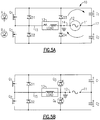
- FIG. 5A A first modification of the voltage and power regulating circuit is shown in Fig. 5A , in which elements that are similar to those in the first embodiment are identified with the same reference characters.
- the power capacitors C1, C2 and electronic switching elements Q1, Q2 are provided, as previously, as are diodes D1 and D2 which are connected in parallel with the power electrodes of the switching elements Q1 an Q2, respectively.
- This embodiment adds two additional diodes D3 and D4 arranged with the anode of diode D3 and the cathode of diode D4 connected together to the neutral terminal 12, the cathode of diode D3 coupled to the upper terminal of capacitor C1 and the anode of diode D4 coupled to the lower terminal of the capacitor C2.
- This arrangement effects a super-boost mode.
- the capacitor C2 charges through the diode D4 as well as charging through the diode D2 and the load; on the negative half-cycle, the capacitor C1 charges through the diode D3 as well as charging through the diode D1 and the load.
- the paths through diode D3 and through diode D4 dominate, as they are the low-impedance pathways. These permit the capacitors C1 and C2 to be charged to peak at the opposite half-cycles.
- FIG. 5B A related modified embodiment is shown in Fig. 5B wherein the elements that are the same as those in the first embodiment are identified with the same reference characters, and a general description of those can be omitted here.
- this arrangement employs thryistors, i.e., SCRs Q3 and Q4 which are respectively connected between the upper plate of capacitor C1 and the neutral terminal 12, and between the terminal 12 and the lower plate of the capacitor C2.
- the capacitors C1, C2 can be charged less than the peak voltage on the reverse half cycles.
- FIG. 5C A further embodiment is illustrated in Fig. 5C , where elements that are the same or similar to those in the earlier embodiment(s) are identified with the same reference numbers.
- FETs or similar types of transistors Q3' and Q4' are employed in place of the thyristors (SCRs) Q3, Q4.
- SCRs thyristors
- multiple charge pulses can be realized by applying a pulsed command signal c or d to the gates of the transistors Q3' and Q4'.
- the respective transistors have a series diode D5, D6, whereas the optional protective diodes D3 and D4 are connected across the power electrodes of the respective transistor.
- the applied load voltage can be regulated, i.e., increased or diminished, by controlling the amount of pre-charge to the capacitors C1 and C2.
- the command signals a , b , c , and d applied to the gates of the transistors Q1, Q2, Q3', and Q4' can appear as shown in the chart of Fig. 6 , where the line voltage wave V Line is also shown for reference purposes.
- the command signals a and b appear as single-pulse (or multiple-pulse) signals on alternate half cycles, as described in reference to previous embodiments.
- the command signals c and d appear as single or as chopped or multiple pulses during alternate half cycles.
- the relative duty cycle can be adjusted to achieve the desired precharge of the capacitors C1 and C2.
- Fig. 7 shows an embodiment of the power regulation circuit of this invention, constructed generally as in Fig. 5 , but here arranged to control application of an auxiliary power source across an AC load 13, and which is also capable of switching excess amounts the auxiliary power onto the source of line current.
- there are two sources of DC power namely, photoelectric solar arrays 23 and 24 with the positive terminal of array 23 applied to a high terminal 21, a negative terminal of the other array 24 applied to a low terminal 22, and the positive terminal of the array 24 connected with the negative terminal of the array 23 at an intermediate voltage, and this is coupled to the hot or black terminal 17 which feeds the center junction of the two capacitors C1 and C2.
- Additional electronic switch elements Q7 and Q8 are interposed between the terminals 21, 22 and the outer plates of the respective capacitors C1 and C2.
- the switch elements Q7 and Q8 are gated ON at or near the zero crossings of the main input AC power wave during opposite half-cycles, and the voltage from the solar arrays 23, 24 is used to pre-charge the capacitors C1 and C2.
- the energy from the solar array, together with the AC line power, is then gated to the load 13 through the switch devices Q1, Q2, Q3', Q4'.
- one or both of the switch elements Q7 and Q8 could be interposed between the respective solar arrays 23, 24 and the terminal 17.
- this circuit could be easily modified by persons skilled in this field to impose the power generated locally (by the solar arrays) onto single-phase or three-phase power.
- This arrangement can be employed with other power source devices as well that extract energy from the natural environment (wind, water, solar, etc.) including wind turbines, water turbines, and geothermal-power generators) of which the solar array would be an example.
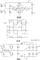
- Fig. 8A is an oscilloscope trace of the applied load voltage where the drive wave is developed in accordance with this invention and is applied to the field winding of an AC induction motor, in a boost mode as discussed in connection with Figs. 1B and 1C .
- This trace is typical of each cycle after the start-up, where the capacitors C1 and C2 have been precharged on the opposite half-cycle.
- Fig. 8A shows both the AC line power wave LINE and the load or applied waveform LOAD.
- a trace of the command signal a is shown also, which has an ON period of phase angle (0 to ⁇ /2 or 0 to 90) during each positive half cycle, followed by an OFF period ⁇ for the remainder of the half cycle.
- the command signal a remains OFF during the opposite, negative half cycle.
- the other command signal b (not shown here) has a similar form, but delayed by 180° (or ⁇ ).
- the resultant applied AC power wave LOAD as shown here has a generally sinusoidal waveform.
- the line voltage has an RMS value of 155 volts
- the applied voltage LOAD has an RMS value of 180 volts. This represents a voltage boost of 25 volts AC.
- a possible implementation of this could be a lightly loaded AC motor.
- Fig. 8B shows a similar chart of a line voltage LINE and load voltage LOAD with the command signals a (shown) and b (not shown) adjusted for increased output voltage.
- the line voltage waveform has an RMS value of 154 volts AC
- the output or applied waveform LOAD has a boosted RMS value of 191 volts AC, i.e., a boost of 37 volts AC, e.g., for a heavily loaded AC motor.
- Fig.8A and Fig. 8B At least some of the power reflected by the reactive load is captured by the capacitors C1 and C2, creating a support level by the precharging of the capacitors C1 and C2, and this is controlled by the command signals a and b .
- This captured energy is then applied on the subsequent half cycle.
- the command signals are generated in response to feedback from the motor (or other reactive load) to optimize motor performance under the existing line and load conditions.
- the waveform, i.e., the duty cycle and phase of the command signals a and b can be varied to achieve a desired boost in voltage, within a fairly broad useful range.
- the applied wave LOAD leads the input wave LINE in phase by a few degrees.
- the circuit of this invention can dynamically control the motor voltage and power in response to variable load conditions and to variable line conditions.
- the reactive elements For the control of motors over a larger power range, e.g., up to five kilowatts, the reactive elements should be sized according to the largest expected load, and then for smaller loads the number, phase, and duty cycles of the command pulses would be selected to produce the sinusoidal load power wave.
- a non-sinusoidal power wave may be more appropriate, e.g., for a non-linear load in which half-cycle torque requirements are variable (such as a reciprocating compressor).
- a more elaborate control scheme may be required in order to tailor the applied power wave to the load requirements and at the same time to enhance both local and grid efficiency.
- the voltage level of the applied voltage LOAD will self-adjust if the imposed mechanical load changes. That is, if the mechanical load increases upon the rotor of the AC induction motor, the electrical load begins to appear more resistive and less reactive, that is, the load phase angle increases and the back EMF drops. This causes more current to flow through the load and capacitors during the OFF phase ⁇ , and as a result the capacitors C1 and C2 will pre-charge more during the OFF phase ⁇ , increasing the applied voltage LOAD accordingly. When the motor again achieves normal run speed, the applied voltage LOAD will be reduced by a similar amount.
- a zero crossing detector 28 senses the timing of zero voltage (or zero current) and the polarity, and a peak voltage detector senses the peak or maximum voltage of the line AC.
- a microprocessor circuit 30 which is suitably programmed to provide the command signals a and b , and for some embodiments the command signals c and d as well.
- a user interface control is represented here as a variable resistance 31, but could instead be a digital input, which could be provided e.g. from a computer device, hand held digital device or user interface.
- the motor drive circuit of this invention can be adapted to drive devices with significant inductive loads, such as air conditioning compressors.
- Fig. 10 represents a simplified expression of the concept of the Fig. 7 embodiment, for example, in which a voltage control and conditioner circuit arrangement 40 is interposed between a source of AC line power 11, 12 and an AC load 13 (e.g., an induction motor), and in which a supplementary DC battery power source 23 (24) such as solar array(s), can be connected to DC input or output terminals of the arrangement.
- the arrangement 40 can include capacitive and switched elements as shown and described, e.g., in Fig. 7 .
- a moderate value AC capacitor 42 can be placed in series in one of the power conductors 11, i.e., interposed between the source of AC line voltage and the AC load 13 (i.e., an induction motor).
- the capacitor is positioned in series with the entire load, i.e., both the run winding R and the start winding S and start capacitor C, so as to affect the power wave applied to each.
- the line voltage should drop from a nominal 220 volts to a brown-out level of 170 volts RMS, and if a moderate-value AC capacitor, e.g, 40 ⁇ f, is used for the capacitor 42, then after the first few cycles the effective power applied to the motor 13 will be between about 205 and 240 volts. This will allow the motor to start and run normally. In this arrangement, some of the power that would normally be reflected back from the motor windings, i.e., (usually expressed as the imaginary component of the complex applied power) is actually stored on the AC capacitor 42, and then is added to the real component of power on the subsequent wave.
- a moderate-value AC capacitor e.g, 40 ⁇ f
- a normally closed shunt or switch 44 bypasses the power around the capacitor 42 as long as the mains AC power is at or above a threshold level, i.e., a normal minimum line voltage level such as 195 volts.
- a low voltage detector 46 is connected to line power conductors 11, 12 to open the switch 44 when the line voltage drops below the threshold level. This arrangement is useful for appliances, such as refrigerators and window air conditioners, which may otherwise become unable to start if the line power quality drops due to heavy use, or due to inability of the electrical power provider to deliver power at proper voltage.
- FIG. 12 An alternative embodiment of the arrangement of Fig. 12 can be configured generally as shown in Fig. 12 .
- an electronic switch e.g., a triac 48
- a control circuit 50 with inputs connected with the input line voltage and the applied load voltage, generates a gating signal that is applied to the electronic switch 48, based on the phase and level of the AC voltage.
- the switch is gated full on, so that the full power wave is boosted, as discussed in connection with the previous embodiment.
- control circuit 50 will turn off the electronic switch 48 for some portion of the cycle, producing an applied voltage power wave as illustrated in Fig. 12A , so that the RMS applied voltage stays within a normal range centered on about 220 volts.
- Fig. 13 illustrates an application of this same arrangement in a polyphase, i.e., three-phase motor application.
- the line power is in the form of three phased components A, B, and C, and is applied to a motor winding 113, here in a delta configuration.
- Two of the three power conductors have a capacitor 42A or 42B and electronic switch 48A or 48B in line with their connection to the motor winding.
- a delta configuration there is no need for a similar capacitor on the third or C-phase power conductor, although a switch and capacitor optionally could be installed on that conductor.
- a capacitor and electronic switch would be present on three legs.
- a control circuit (not shown here) would be similar in function to that element in the Fig. 12 embodiment.
- DC capacitors could be substituted for the AC capacitor 40. In that case, there would be a set of one DC capacitor and one diode conducting in one direction, and another set of a DC capacitor and diode conducting in the opposite direction, that is, in anti-parallel with the first set.
- Fig. 14 is a general schematic showing leads 11 and 12 connecting an AC source of AC line voltage to a complex reactive load 13, such as an induction motor, which has resistive, inductive, and capacitive components, and which will reflect at least some of the incoming AC power that is applied to it.
- the basic improvement concept here is to employ an intervening synthetic AC wave source 52 in line between the line source and the load 13, which will generate supplemental AC voltage that adds to the line waveform to optimize the phase and voltage level.
- a control signal generator e.g., the microprocessor 30 of Fig.
- the intervening synthetic AC source is implemented as a reactive element 521', as shown in Fig. 15 , which is switched in and out in accordance with command signals from the control signal generator 30.
- the disclosure of those preferred embodiments does not foreclose other possibilities in the implementation of the intervening synthetic AC source.
Landscapes
- Engineering & Computer Science (AREA)
- Power Engineering (AREA)
- Inverter Devices (AREA)
- Control Of Ac Motors In General (AREA)
- Control Of Electrical Variables (AREA)
Applications Claiming Priority (2)
| Application Number | Priority Date | Filing Date | Title |
|---|---|---|---|
| US13/037,807 US8093858B1 (en) | 2011-03-01 | 2011-03-01 | AC line voltage conditioner and controller |
| EP12154686.5A EP2495857B1 (de) | 2011-03-01 | 2012-02-09 | Spannungskonditionierer und -steuerung für Wechselstromleitung |
Related Parent Applications (1)
| Application Number | Title | Priority Date | Filing Date |
|---|---|---|---|
| EP12154686.5A Division EP2495857B1 (de) | 2011-03-01 | 2012-02-09 | Spannungskonditionierer und -steuerung für Wechselstromleitung |
Publications (1)
| Publication Number | Publication Date |
|---|---|
| EP3657665A1 true EP3657665A1 (de) | 2020-05-27 |
Family
ID=45419111
Family Applications (4)
| Application Number | Title | Priority Date | Filing Date |
|---|---|---|---|
| EP12154686.5A Active EP2495857B1 (de) | 2011-03-01 | 2012-02-09 | Spannungskonditionierer und -steuerung für Wechselstromleitung |
| EP20151669.7A Withdrawn EP3657665A1 (de) | 2011-03-01 | 2012-02-09 | Spannungskonditionierer und steuergerät für wechselstromleitung |
| EP19185191.4A Withdrawn EP3573225A1 (de) | 2011-03-01 | 2012-02-09 | Spannungskonditionierer und steuergerät für wechselstromleitung |
| EP20170911.0A Withdrawn EP3703233A1 (de) | 2011-03-01 | 2012-02-09 | Spannungskonditionierer und steuergerät für wechselstromleitung |
Family Applications Before (1)
| Application Number | Title | Priority Date | Filing Date |
|---|---|---|---|
| EP12154686.5A Active EP2495857B1 (de) | 2011-03-01 | 2012-02-09 | Spannungskonditionierer und -steuerung für Wechselstromleitung |
Family Applications After (2)
| Application Number | Title | Priority Date | Filing Date |
|---|---|---|---|
| EP19185191.4A Withdrawn EP3573225A1 (de) | 2011-03-01 | 2012-02-09 | Spannungskonditionierer und steuergerät für wechselstromleitung |
| EP20170911.0A Withdrawn EP3703233A1 (de) | 2011-03-01 | 2012-02-09 | Spannungskonditionierer und steuergerät für wechselstromleitung |
Country Status (5)
| Country | Link |
|---|---|
| US (1) | US8093858B1 (de) |
| EP (4) | EP2495857B1 (de) |
| JP (1) | JP6080366B2 (de) |
| BR (2) | BR102012004428B8 (de) |
| ES (1) | ES2773021T3 (de) |
Families Citing this family (23)
| Publication number | Priority date | Publication date | Assignee | Title |
|---|---|---|---|---|
| GB201006388D0 (en) | 2010-04-16 | 2010-06-02 | Dyson Technology Ltd | Control of brushless motor |
| GB201006396D0 (en) | 2010-04-16 | 2010-06-02 | Dyson Technology Ltd | Control of a brushless motor |
| GB201006391D0 (en) | 2010-04-16 | 2010-06-02 | Dyson Technology Ltd | Control of a brushless permanent-magnet motor |
| GB201006395D0 (en) | 2010-04-16 | 2010-06-02 | Dyson Technology Ltd | Control of a brushless motor |
| GB201006397D0 (en) | 2010-04-16 | 2010-06-02 | Dyson Technology Ltd | Control of a brushless motor |
| GB201006387D0 (en) * | 2010-04-16 | 2010-06-02 | Dyson Technology Ltd | Control of a brushless motor |
| GB201006392D0 (en) | 2010-04-16 | 2010-06-02 | Dyson Technology Ltd | Controller for a brushless motor |
| GB201006390D0 (en) | 2010-04-16 | 2010-06-02 | Dyson Technology Ltd | Control of a brushless motor |
| GB201006386D0 (en) | 2010-04-16 | 2010-06-02 | Dyson Technology Ltd | Control of a brushless motor |
| GB201006384D0 (en) * | 2010-04-16 | 2010-06-02 | Dyson Technology Ltd | Control of a brushless motor |
| GB201006398D0 (en) | 2010-04-16 | 2010-06-02 | Dyson Technology Ltd | Control of a brushless motor |
| GB2484289B (en) | 2010-10-04 | 2013-11-20 | Dyson Technology Ltd | Control of an electrical machine |
| US8362735B2 (en) * | 2011-03-07 | 2013-01-29 | Protective Energy Economizer Technology | Single phase motor energy economizer for regulating the use of electricity |
| US20130002230A1 (en) * | 2011-06-28 | 2013-01-03 | Progress Rail Services Corp. | Ac load soft start for variable-frequency power source |
| JP5883834B2 (ja) | 2013-08-08 | 2016-03-15 | 東芝テック株式会社 | 電力変換装置 |
| CN104300800A (zh) * | 2014-06-05 | 2015-01-21 | 董振隆 | 一种移相电源 |
| WO2016111768A1 (en) * | 2015-01-09 | 2016-07-14 | V Square/R Llc | Dynamic power control for induction motors |
| US10097003B2 (en) * | 2015-07-06 | 2018-10-09 | Kartik Nanda | System and method for managing the delivery of electric power |
| US10267532B2 (en) * | 2016-10-31 | 2019-04-23 | International Controls And Measurements Corporation | Thermostat with power stealing |
| US10461632B1 (en) * | 2018-04-10 | 2019-10-29 | Semiconductor Components Industries, Llc | Current sensing for bridgeless PFC converters |
| CN113016113B (zh) | 2018-11-15 | 2024-09-20 | 茵梦达有限责任公司 | 无输入功率的变频驱动器的延长制动 |
| JP7143272B2 (ja) * | 2019-12-24 | 2022-09-28 | ツインバード工業株式会社 | フリーピストン型スターリング冷凍機 |
| KR102916393B1 (ko) | 2020-07-20 | 2026-01-23 | 삼성전자주식회사 | 전자 장치 및 그 제어 방법 |
Citations (5)
| Publication number | Priority date | Publication date | Assignee | Title |
|---|---|---|---|---|
| US4459528A (en) | 1982-12-16 | 1984-07-10 | The United States Of America As Represented By The Administrator Of The National Aeronautics And Space Administration | Phase detector for three-phase power factor controller |
| WO1998025849A1 (en) * | 1996-12-11 | 1998-06-18 | Hitachi, Ltd. | Elevator control device and control device for power converter |
| US6121749A (en) * | 1998-05-11 | 2000-09-19 | Work Smart Energy Enterprises, Inc. | Variable-speed drive for single-phase motors |
| US20030122433A1 (en) | 2000-07-25 | 2003-07-03 | Bach Daniel G. | Power factor control of an induction motor |
| US20080218917A1 (en) * | 2007-03-08 | 2008-09-11 | Archer William A | Methods and systems for operating direct current motors |
Family Cites Families (19)
| Publication number | Priority date | Publication date | Assignee | Title |
|---|---|---|---|---|
| US4651265A (en) * | 1985-07-29 | 1987-03-17 | Westinghouse Electric Corp. | Active power conditioner system |
| US4706180A (en) * | 1985-11-29 | 1987-11-10 | York International Corporation | Pulse width modulated inverter system for driving single phase a-c induction motor |
| US4933798A (en) * | 1987-10-22 | 1990-06-12 | Widmayer R&D Ventures | Self protecting and automatic resetting capacitor synchronous switch apparatus for control of AC power to inductive loads |
| JP3054954B2 (ja) * | 1990-07-24 | 2000-06-19 | 国華 王 | コンデンサー交流昇圧回路 |
| US5583423A (en) * | 1993-11-22 | 1996-12-10 | Bangerter; Fred F. | Energy saving power control method |
| US5831410A (en) | 1994-11-04 | 1998-11-03 | Allen Bradley Company, Inc. | Apparatus used with AC motors for eliminating line voltage reflections |
| US5883490A (en) * | 1996-06-14 | 1999-03-16 | Moreira; Julio C. | Electric motor controller and method |
| JPH1084696A (ja) * | 1996-07-16 | 1998-03-31 | Hitachi Ltd | 空気調和機 |
| US6420801B1 (en) | 2000-04-11 | 2002-07-16 | Electro Industries, Inc. | Alternative power supply connection |
| US20030095421A1 (en) | 2000-05-23 | 2003-05-22 | Kadatskyy Anatoly F. | Power factor correction circuit |
| US20030034753A1 (en) | 2001-08-14 | 2003-02-20 | Heimbaugh Ashley R. | Constant torque AC induction motor controller |
| US6753670B2 (en) | 2002-03-06 | 2004-06-22 | Andrew S. Kadah | Universal energy regulating controller circuit |
| JP2003284341A (ja) * | 2002-03-25 | 2003-10-03 | Mitsubishi Electric Corp | 交流電圧調整装置 |
| US7091707B2 (en) | 2003-09-29 | 2006-08-15 | Xantrex Technology, Inc. | Method and apparatus for controlling power drawn from an energy converter |
| JP4097034B2 (ja) * | 2004-02-24 | 2008-06-04 | 株式会社センサータ・テクノロジーズジャパン | 省電力化モータ起動装置 |
| US7190125B2 (en) * | 2004-07-15 | 2007-03-13 | Lutron Electronics Co., Inc. | Programmable wallbox dimmer |
| WO2006013557A2 (en) | 2004-08-02 | 2006-02-09 | Green Power Technologies Ltd. | Method and control circuitry for improved-performance switch-mode converters |
| US20060126240A1 (en) | 2004-12-10 | 2006-06-15 | Xantrex International | AC power backfeed protection based on voltage |
| US20090293523A1 (en) * | 2008-06-02 | 2009-12-03 | Dover Systems, Inc. | System and method for using a photovoltaic power source with a secondary coolant refrigeration system |
-
2011
- 2011-03-01 US US13/037,807 patent/US8093858B1/en active Active
-
2012
- 2012-02-09 EP EP12154686.5A patent/EP2495857B1/de active Active
- 2012-02-09 EP EP20151669.7A patent/EP3657665A1/de not_active Withdrawn
- 2012-02-09 ES ES12154686T patent/ES2773021T3/es active Active
- 2012-02-09 EP EP19185191.4A patent/EP3573225A1/de not_active Withdrawn
- 2012-02-09 EP EP20170911.0A patent/EP3703233A1/de not_active Withdrawn
- 2012-02-28 BR BR102012004428A patent/BR102012004428B8/pt not_active IP Right Cessation
- 2012-02-28 BR BR122020011567-0A patent/BR122020011567B1/pt active IP Right Grant
- 2012-02-28 JP JP2012040895A patent/JP6080366B2/ja not_active Expired - Fee Related
Patent Citations (5)
| Publication number | Priority date | Publication date | Assignee | Title |
|---|---|---|---|---|
| US4459528A (en) | 1982-12-16 | 1984-07-10 | The United States Of America As Represented By The Administrator Of The National Aeronautics And Space Administration | Phase detector for three-phase power factor controller |
| WO1998025849A1 (en) * | 1996-12-11 | 1998-06-18 | Hitachi, Ltd. | Elevator control device and control device for power converter |
| US6121749A (en) * | 1998-05-11 | 2000-09-19 | Work Smart Energy Enterprises, Inc. | Variable-speed drive for single-phase motors |
| US20030122433A1 (en) | 2000-07-25 | 2003-07-03 | Bach Daniel G. | Power factor control of an induction motor |
| US20080218917A1 (en) * | 2007-03-08 | 2008-09-11 | Archer William A | Methods and systems for operating direct current motors |
Also Published As
| Publication number | Publication date |
|---|---|
| JP6080366B2 (ja) | 2017-02-15 |
| BR102012004428A2 (pt) | 2013-07-23 |
| ES2773021T3 (es) | 2020-07-09 |
| BR102012004428B1 (pt) | 2021-04-20 |
| BR122020011567B1 (pt) | 2021-01-26 |
| EP2495857A2 (de) | 2012-09-05 |
| EP3703233A1 (de) | 2020-09-02 |
| EP2495857A3 (de) | 2017-07-05 |
| EP3573225A1 (de) | 2019-11-27 |
| BR102012004428B8 (pt) | 2021-11-30 |
| US8093858B1 (en) | 2012-01-10 |
| JP2012182982A (ja) | 2012-09-20 |
| EP2495857B1 (de) | 2020-01-15 |
Similar Documents
| Publication | Publication Date | Title |
|---|---|---|
| US8093858B1 (en) | AC line voltage conditioner and controller | |
| US20250158512A1 (en) | DC to AC Converter for Solar Energy System | |
| EP2430506B1 (de) | Eine motorsteuerung und ein zugehöriges verfahren | |
| Steigerwald et al. | Application of power transistors to residential and intermediate rating photovoltaic array power conditioners | |
| Mishra et al. | An efficient control scheme of self-reliant solar-powered water pumping system using a three-level DC–DC converter | |
| US10211640B2 (en) | Adaptive load sharing system | |
| US11923787B2 (en) | Isolated inverters | |
| EP2807716A1 (de) | Schaltung zur leistungsübertragung zwischen gleichstrom und einer leitung mit wechselstrom | |
| CN106605358A (zh) | 能源节省高频串联降压交流电压稳压器系统 | |
| Fukuda et al. | An auxiliary-supply-assisted harmonic reduction scheme for 12-pulse diode rectifiers | |
| US20080074076A1 (en) | Power control for induction motors using variable frequency AC power | |
| Sanhueza et al. | Analysis and evaluation of residential air conditioners for power system studies | |
| HK40035920A (en) | Ac line voltage conditioner and controller | |
| HK40028993A (en) | Ac line voltage conditioner and controller | |
| CN108574293A (zh) | 一种补偿不平衡电网负载的控制方法 | |
| Oshima et al. | Mega Solar PCS Incorporating All-SiC Module “PVI1000 AJ-3/1000” | |
| Arvindan et al. | Power Quality Analysis Of Six-And Twelve-Pulse Rectifiers As Series Cascaded Topologies Of The Three-Pulse Rectifier | |
| CN109600059A (zh) | 一种直流母线电压的软启动电路 | |
| CN102780445B (zh) | 绕线式异步电动机复式交流斩波调速 | |
| Dos Reis et al. | Harmonic mitigation in wind turbine energy conversion systems | |
| CN214544153U (zh) | 一种高压交流电动机可调降压软启动装置 | |
| Ball et al. | Static power converters of 500 kW or less serving as the relay interface package for nonconventional generators | |
| Louie | Off-Grid System DC Converters and Rectifiers | |
| Louie | Off-Grid System Converters and Controllers |
Legal Events
| Date | Code | Title | Description |
|---|---|---|---|
| PUAI | Public reference made under article 153(3) epc to a published international application that has entered the european phase |
Free format text: ORIGINAL CODE: 0009012 |
|
| AC | Divisional application: reference to earlier application |
Ref document number: 2495857 Country of ref document: EP Kind code of ref document: P |
|
| AK | Designated contracting states |
Kind code of ref document: A1 Designated state(s): AL AT BE BG CH CY CZ DE DK EE ES FI FR GB GR HR HU IE IS IT LI LT LU LV MC MK MT NL NO PL PT RO RS SE SI SK SM TR |
|
| STAA | Information on the status of an ep patent application or granted ep patent |
Free format text: STATUS: REQUEST FOR EXAMINATION WAS MADE |
|
| 17P | Request for examination filed |
Effective date: 20201126 |
|
| RBV | Designated contracting states (corrected) |
Designated state(s): AL AT BE BG CH CY CZ DE DK EE ES FI FR GB GR HR HU IE IS IT LI LT LU LV MC MK MT NL NO PL PT RO RS SE SI SK SM TR |
|
| REG | Reference to a national code |
Ref country code: HK Ref legal event code: DE Ref document number: 40028993 Country of ref document: HK |
|
| 18W | Application withdrawn |
Effective date: 20210318 |