EP3661337A1 - Carte de circuit imprimé en céramique et son procédé de production - Google Patents
Carte de circuit imprimé en céramique et son procédé de production Download PDFInfo
- Publication number
- EP3661337A1 EP3661337A1 EP18839092.6A EP18839092A EP3661337A1 EP 3661337 A1 EP3661337 A1 EP 3661337A1 EP 18839092 A EP18839092 A EP 18839092A EP 3661337 A1 EP3661337 A1 EP 3661337A1
- Authority
- EP
- European Patent Office
- Prior art keywords
- braze material
- powder
- ceramic
- bonding
- substrate
- Prior art date
- Legal status (The legal status is an assumption and is not a legal conclusion. Google has not performed a legal analysis and makes no representation as to the accuracy of the status listed.)
- Granted
Links
Images
Classifications
-
- H—ELECTRICITY
- H05—ELECTRIC TECHNIQUES NOT OTHERWISE PROVIDED FOR
- H05K—PRINTED CIRCUITS; CASINGS OR CONSTRUCTIONAL DETAILS OF ELECTRIC APPARATUS; MANUFACTURE OF ASSEMBLAGES OF ELECTRICAL COMPONENTS
- H05K3/00—Apparatus or processes for manufacturing printed circuits
- H05K3/38—Improvement of the adhesion between the insulating substrate and the metal
- H05K3/388—Improvement of the adhesion between the insulating substrate and the metal by the use of a metallic or inorganic thin film adhesion layer
-
- H—ELECTRICITY
- H05—ELECTRIC TECHNIQUES NOT OTHERWISE PROVIDED FOR
- H05K—PRINTED CIRCUITS; CASINGS OR CONSTRUCTIONAL DETAILS OF ELECTRIC APPARATUS; MANUFACTURE OF ASSEMBLAGES OF ELECTRICAL COMPONENTS
- H05K1/00—Printed circuits
- H05K1/02—Details
- H05K1/03—Use of materials for the substrate
- H05K1/0306—Inorganic insulating substrates, e.g. ceramic, glass
-
- B—PERFORMING OPERATIONS; TRANSPORTING
- B23—MACHINE TOOLS; METAL-WORKING NOT OTHERWISE PROVIDED FOR
- B23K—SOLDERING OR UNSOLDERING; WELDING; CLADDING OR PLATING BY SOLDERING OR WELDING; CUTTING BY APPLYING HEAT LOCALLY, e.g. FLAME CUTTING; WORKING BY LASER BEAM
- B23K1/00—Soldering, e.g. brazing, or unsoldering
-
- B—PERFORMING OPERATIONS; TRANSPORTING
- B23—MACHINE TOOLS; METAL-WORKING NOT OTHERWISE PROVIDED FOR
- B23K—SOLDERING OR UNSOLDERING; WELDING; CLADDING OR PLATING BY SOLDERING OR WELDING; CUTTING BY APPLYING HEAT LOCALLY, e.g. FLAME CUTTING; WORKING BY LASER BEAM
- B23K1/00—Soldering, e.g. brazing, or unsoldering
- B23K1/19—Soldering, e.g. brazing, or unsoldering taking account of the properties of the materials to be soldered
-
- B—PERFORMING OPERATIONS; TRANSPORTING
- B23—MACHINE TOOLS; METAL-WORKING NOT OTHERWISE PROVIDED FOR
- B23K—SOLDERING OR UNSOLDERING; WELDING; CLADDING OR PLATING BY SOLDERING OR WELDING; CUTTING BY APPLYING HEAT LOCALLY, e.g. FLAME CUTTING; WORKING BY LASER BEAM
- B23K35/00—Rods, electrodes, materials, or media, for use in soldering, welding, or cutting
- B23K35/02—Rods, electrodes, materials, or media, for use in soldering, welding, or cutting characterised by mechanical features, e.g. shape
- B23K35/0222—Rods, electrodes, materials, or media, for use in soldering, welding, or cutting characterised by mechanical features, e.g. shape for use in soldering or brazing
- B23K35/0244—Powders, particles or spheres; Preforms made therefrom
-
- B—PERFORMING OPERATIONS; TRANSPORTING
- B23—MACHINE TOOLS; METAL-WORKING NOT OTHERWISE PROVIDED FOR
- B23K—SOLDERING OR UNSOLDERING; WELDING; CLADDING OR PLATING BY SOLDERING OR WELDING; CUTTING BY APPLYING HEAT LOCALLY, e.g. FLAME CUTTING; WORKING BY LASER BEAM
- B23K35/00—Rods, electrodes, materials, or media, for use in soldering, welding, or cutting
- B23K35/22—Rods, electrodes, materials, or media, for use in soldering, welding, or cutting characterised by the composition or nature of the material
- B23K35/24—Selection of soldering or welding materials proper
- B23K35/30—Selection of soldering or welding materials proper with the principal constituent melting at less than 1550°C
- B23K35/3006—Ag as the principal constituent
-
- C—CHEMISTRY; METALLURGY
- C04—CEMENTS; CONCRETE; ARTIFICIAL STONE; CERAMICS; REFRACTORIES
- C04B—LIME, MAGNESIA; SLAG; CEMENTS; COMPOSITIONS THEREOF, e.g. MORTARS, CONCRETE OR LIKE BUILDING MATERIALS; ARTIFICIAL STONE; CERAMICS; REFRACTORIES; TREATMENT OF NATURAL STONE
- C04B37/00—Joining burned ceramic articles with other burned ceramic articles or other articles by heating
- C04B37/003—Joining burned ceramic articles with other burned ceramic articles or other articles by heating by means of an interlayer consisting of a combination of materials selected from glass, or ceramic material with metals, metal oxides or metal salts
- C04B37/006—Joining burned ceramic articles with other burned ceramic articles or other articles by heating by means of an interlayer consisting of a combination of materials selected from glass, or ceramic material with metals, metal oxides or metal salts consisting of metals or metal salts
-
- C—CHEMISTRY; METALLURGY
- C04—CEMENTS; CONCRETE; ARTIFICIAL STONE; CERAMICS; REFRACTORIES
- C04B—LIME, MAGNESIA; SLAG; CEMENTS; COMPOSITIONS THEREOF, e.g. MORTARS, CONCRETE OR LIKE BUILDING MATERIALS; ARTIFICIAL STONE; CERAMICS; REFRACTORIES; TREATMENT OF NATURAL STONE
- C04B37/00—Joining burned ceramic articles with other burned ceramic articles or other articles by heating
- C04B37/02—Joining burned ceramic articles with other burned ceramic articles or other articles by heating with metallic articles
- C04B37/023—Joining burned ceramic articles with other burned ceramic articles or other articles by heating with metallic articles characterised by the interlayer used
- C04B37/026—Joining burned ceramic articles with other burned ceramic articles or other articles by heating with metallic articles characterised by the interlayer used consisting of metals or metal salts
-
- C—CHEMISTRY; METALLURGY
- C22—METALLURGY; FERROUS OR NON-FERROUS ALLOYS; TREATMENT OF ALLOYS OR NON-FERROUS METALS
- C22C—ALLOYS
- C22C5/00—Alloys based on noble metals
- C22C5/06—Alloys based on silver
-
- C—CHEMISTRY; METALLURGY
- C22—METALLURGY; FERROUS OR NON-FERROUS ALLOYS; TREATMENT OF ALLOYS OR NON-FERROUS METALS
- C22C—ALLOYS
- C22C5/00—Alloys based on noble metals
- C22C5/06—Alloys based on silver
- C22C5/08—Alloys based on silver with copper as the next major constituent
-
- H—ELECTRICITY
- H05—ELECTRIC TECHNIQUES NOT OTHERWISE PROVIDED FOR
- H05K—PRINTED CIRCUITS; CASINGS OR CONSTRUCTIONAL DETAILS OF ELECTRIC APPARATUS; MANUFACTURE OF ASSEMBLAGES OF ELECTRICAL COMPONENTS
- H05K1/00—Printed circuits
- H05K1/02—Details
- H05K1/09—Use of materials for the conductive, e.g. metallic pattern
-
- H—ELECTRICITY
- H05—ELECTRIC TECHNIQUES NOT OTHERWISE PROVIDED FOR
- H05K—PRINTED CIRCUITS; CASINGS OR CONSTRUCTIONAL DETAILS OF ELECTRIC APPARATUS; MANUFACTURE OF ASSEMBLAGES OF ELECTRICAL COMPONENTS
- H05K3/00—Apparatus or processes for manufacturing printed circuits
- H05K3/10—Apparatus or processes for manufacturing printed circuits in which conductive material is applied to the insulating support in such a manner as to form the desired conductive pattern
- H05K3/102—Apparatus or processes for manufacturing printed circuits in which conductive material is applied to the insulating support in such a manner as to form the desired conductive pattern by bonding of conductive powder, i.e. metallic powder
-
- H—ELECTRICITY
- H05—ELECTRIC TECHNIQUES NOT OTHERWISE PROVIDED FOR
- H05K—PRINTED CIRCUITS; CASINGS OR CONSTRUCTIONAL DETAILS OF ELECTRIC APPARATUS; MANUFACTURE OF ASSEMBLAGES OF ELECTRICAL COMPONENTS
- H05K3/00—Apparatus or processes for manufacturing printed circuits
- H05K3/38—Improvement of the adhesion between the insulating substrate and the metal
- H05K3/381—Improvement of the adhesion between the insulating substrate and the metal by special treatment of the substrate
-
- H—ELECTRICITY
- H10—SEMICONDUCTOR DEVICES; ELECTRIC SOLID-STATE DEVICES NOT OTHERWISE PROVIDED FOR
- H10W—GENERIC PACKAGES, INTERCONNECTIONS, CONNECTORS OR OTHER CONSTRUCTIONAL DETAILS OF DEVICES COVERED BY CLASS H10
- H10W40/00—Arrangements for thermal protection or thermal control
- H10W40/20—Arrangements for cooling
- H10W40/25—Arrangements for cooling characterised by their materials
- H10W40/255—Arrangements for cooling characterised by their materials having a laminate or multilayered structure, e.g. direct bond copper [DBC] ceramic substrates
-
- H—ELECTRICITY
- H10—SEMICONDUCTOR DEVICES; ELECTRIC SOLID-STATE DEVICES NOT OTHERWISE PROVIDED FOR
- H10W—GENERIC PACKAGES, INTERCONNECTIONS, CONNECTORS OR OTHER CONSTRUCTIONAL DETAILS OF DEVICES COVERED BY CLASS H10
- H10W70/00—Package substrates; Interposers; Redistribution layers [RDL]
- H10W70/60—Insulating or insulated package substrates; Interposers; Redistribution layers
- H10W70/67—Insulating or insulated package substrates; Interposers; Redistribution layers characterised by their insulating layers or insulating parts
- H10W70/68—Shapes or dispositions thereof
-
- H—ELECTRICITY
- H10—SEMICONDUCTOR DEVICES; ELECTRIC SOLID-STATE DEVICES NOT OTHERWISE PROVIDED FOR
- H10W—GENERIC PACKAGES, INTERCONNECTIONS, CONNECTORS OR OTHER CONSTRUCTIONAL DETAILS OF DEVICES COVERED BY CLASS H10
- H10W70/00—Package substrates; Interposers; Redistribution layers [RDL]
- H10W70/60—Insulating or insulated package substrates; Interposers; Redistribution layers
- H10W70/67—Insulating or insulated package substrates; Interposers; Redistribution layers characterised by their insulating layers or insulating parts
- H10W70/69—Insulating materials thereof
- H10W70/692—Ceramics or glasses
-
- C—CHEMISTRY; METALLURGY
- C04—CEMENTS; CONCRETE; ARTIFICIAL STONE; CERAMICS; REFRACTORIES
- C04B—LIME, MAGNESIA; SLAG; CEMENTS; COMPOSITIONS THEREOF, e.g. MORTARS, CONCRETE OR LIKE BUILDING MATERIALS; ARTIFICIAL STONE; CERAMICS; REFRACTORIES; TREATMENT OF NATURAL STONE
- C04B2237/00—Aspects relating to ceramic laminates or to joining of ceramic articles with other articles by heating
- C04B2237/02—Aspects relating to interlayers, e.g. used to join ceramic articles with other articles by heating
- C04B2237/12—Metallic interlayers
- C04B2237/125—Metallic interlayers based on noble metals, e.g. silver
-
- C—CHEMISTRY; METALLURGY
- C04—CEMENTS; CONCRETE; ARTIFICIAL STONE; CERAMICS; REFRACTORIES
- C04B—LIME, MAGNESIA; SLAG; CEMENTS; COMPOSITIONS THEREOF, e.g. MORTARS, CONCRETE OR LIKE BUILDING MATERIALS; ARTIFICIAL STONE; CERAMICS; REFRACTORIES; TREATMENT OF NATURAL STONE
- C04B2237/00—Aspects relating to ceramic laminates or to joining of ceramic articles with other articles by heating
- C04B2237/02—Aspects relating to interlayers, e.g. used to join ceramic articles with other articles by heating
- C04B2237/12—Metallic interlayers
- C04B2237/126—Metallic interlayers wherein the active component for bonding is not the largest fraction of the interlayer
- C04B2237/127—The active component for bonding being a refractory metal
-
- C—CHEMISTRY; METALLURGY
- C04—CEMENTS; CONCRETE; ARTIFICIAL STONE; CERAMICS; REFRACTORIES
- C04B—LIME, MAGNESIA; SLAG; CEMENTS; COMPOSITIONS THEREOF, e.g. MORTARS, CONCRETE OR LIKE BUILDING MATERIALS; ARTIFICIAL STONE; CERAMICS; REFRACTORIES; TREATMENT OF NATURAL STONE
- C04B2237/00—Aspects relating to ceramic laminates or to joining of ceramic articles with other articles by heating
- C04B2237/30—Composition of layers of ceramic laminates or of ceramic or metallic articles to be joined by heating, e.g. Si substrates
- C04B2237/32—Ceramic
- C04B2237/34—Oxidic
- C04B2237/343—Alumina or aluminates
-
- C—CHEMISTRY; METALLURGY
- C04—CEMENTS; CONCRETE; ARTIFICIAL STONE; CERAMICS; REFRACTORIES
- C04B—LIME, MAGNESIA; SLAG; CEMENTS; COMPOSITIONS THEREOF, e.g. MORTARS, CONCRETE OR LIKE BUILDING MATERIALS; ARTIFICIAL STONE; CERAMICS; REFRACTORIES; TREATMENT OF NATURAL STONE
- C04B2237/00—Aspects relating to ceramic laminates or to joining of ceramic articles with other articles by heating
- C04B2237/30—Composition of layers of ceramic laminates or of ceramic or metallic articles to be joined by heating, e.g. Si substrates
- C04B2237/32—Ceramic
- C04B2237/34—Oxidic
- C04B2237/345—Refractory metal oxides
- C04B2237/348—Zirconia, hafnia, zirconates or hafnates
-
- C—CHEMISTRY; METALLURGY
- C04—CEMENTS; CONCRETE; ARTIFICIAL STONE; CERAMICS; REFRACTORIES
- C04B—LIME, MAGNESIA; SLAG; CEMENTS; COMPOSITIONS THEREOF, e.g. MORTARS, CONCRETE OR LIKE BUILDING MATERIALS; ARTIFICIAL STONE; CERAMICS; REFRACTORIES; TREATMENT OF NATURAL STONE
- C04B2237/00—Aspects relating to ceramic laminates or to joining of ceramic articles with other articles by heating
- C04B2237/30—Composition of layers of ceramic laminates or of ceramic or metallic articles to be joined by heating, e.g. Si substrates
- C04B2237/32—Ceramic
- C04B2237/36—Non-oxidic
-
- C—CHEMISTRY; METALLURGY
- C04—CEMENTS; CONCRETE; ARTIFICIAL STONE; CERAMICS; REFRACTORIES
- C04B—LIME, MAGNESIA; SLAG; CEMENTS; COMPOSITIONS THEREOF, e.g. MORTARS, CONCRETE OR LIKE BUILDING MATERIALS; ARTIFICIAL STONE; CERAMICS; REFRACTORIES; TREATMENT OF NATURAL STONE
- C04B2237/00—Aspects relating to ceramic laminates or to joining of ceramic articles with other articles by heating
- C04B2237/30—Composition of layers of ceramic laminates or of ceramic or metallic articles to be joined by heating, e.g. Si substrates
- C04B2237/32—Ceramic
- C04B2237/36—Non-oxidic
- C04B2237/365—Silicon carbide
-
- C—CHEMISTRY; METALLURGY
- C04—CEMENTS; CONCRETE; ARTIFICIAL STONE; CERAMICS; REFRACTORIES
- C04B—LIME, MAGNESIA; SLAG; CEMENTS; COMPOSITIONS THEREOF, e.g. MORTARS, CONCRETE OR LIKE BUILDING MATERIALS; ARTIFICIAL STONE; CERAMICS; REFRACTORIES; TREATMENT OF NATURAL STONE
- C04B2237/00—Aspects relating to ceramic laminates or to joining of ceramic articles with other articles by heating
- C04B2237/30—Composition of layers of ceramic laminates or of ceramic or metallic articles to be joined by heating, e.g. Si substrates
- C04B2237/32—Ceramic
- C04B2237/36—Non-oxidic
- C04B2237/366—Aluminium nitride
-
- C—CHEMISTRY; METALLURGY
- C04—CEMENTS; CONCRETE; ARTIFICIAL STONE; CERAMICS; REFRACTORIES
- C04B—LIME, MAGNESIA; SLAG; CEMENTS; COMPOSITIONS THEREOF, e.g. MORTARS, CONCRETE OR LIKE BUILDING MATERIALS; ARTIFICIAL STONE; CERAMICS; REFRACTORIES; TREATMENT OF NATURAL STONE
- C04B2237/00—Aspects relating to ceramic laminates or to joining of ceramic articles with other articles by heating
- C04B2237/30—Composition of layers of ceramic laminates or of ceramic or metallic articles to be joined by heating, e.g. Si substrates
- C04B2237/32—Ceramic
- C04B2237/36—Non-oxidic
- C04B2237/368—Silicon nitride
-
- C—CHEMISTRY; METALLURGY
- C04—CEMENTS; CONCRETE; ARTIFICIAL STONE; CERAMICS; REFRACTORIES
- C04B—LIME, MAGNESIA; SLAG; CEMENTS; COMPOSITIONS THEREOF, e.g. MORTARS, CONCRETE OR LIKE BUILDING MATERIALS; ARTIFICIAL STONE; CERAMICS; REFRACTORIES; TREATMENT OF NATURAL STONE
- C04B2237/00—Aspects relating to ceramic laminates or to joining of ceramic articles with other articles by heating
- C04B2237/30—Composition of layers of ceramic laminates or of ceramic or metallic articles to be joined by heating, e.g. Si substrates
- C04B2237/40—Metallic
- C04B2237/407—Copper
-
- C—CHEMISTRY; METALLURGY
- C04—CEMENTS; CONCRETE; ARTIFICIAL STONE; CERAMICS; REFRACTORIES
- C04B—LIME, MAGNESIA; SLAG; CEMENTS; COMPOSITIONS THEREOF, e.g. MORTARS, CONCRETE OR LIKE BUILDING MATERIALS; ARTIFICIAL STONE; CERAMICS; REFRACTORIES; TREATMENT OF NATURAL STONE
- C04B2237/00—Aspects relating to ceramic laminates or to joining of ceramic articles with other articles by heating
- C04B2237/50—Processing aspects relating to ceramic laminates or to the joining of ceramic articles with other articles by heating
- C04B2237/59—Aspects relating to the structure of the interlayer
-
- C—CHEMISTRY; METALLURGY
- C04—CEMENTS; CONCRETE; ARTIFICIAL STONE; CERAMICS; REFRACTORIES
- C04B—LIME, MAGNESIA; SLAG; CEMENTS; COMPOSITIONS THEREOF, e.g. MORTARS, CONCRETE OR LIKE BUILDING MATERIALS; ARTIFICIAL STONE; CERAMICS; REFRACTORIES; TREATMENT OF NATURAL STONE
- C04B2237/00—Aspects relating to ceramic laminates or to joining of ceramic articles with other articles by heating
- C04B2237/50—Processing aspects relating to ceramic laminates or to the joining of ceramic articles with other articles by heating
- C04B2237/88—Joining of two substrates, where a substantial part of the joining material is present outside of the joint, leading to an outside joining of the joint
-
- H—ELECTRICITY
- H05—ELECTRIC TECHNIQUES NOT OTHERWISE PROVIDED FOR
- H05K—PRINTED CIRCUITS; CASINGS OR CONSTRUCTIONAL DETAILS OF ELECTRIC APPARATUS; MANUFACTURE OF ASSEMBLAGES OF ELECTRICAL COMPONENTS
- H05K1/00—Printed circuits
- H05K1/02—Details
- H05K1/0271—Arrangements for reducing stress or warp in rigid printed circuit boards, e.g. caused by loads, vibrations or differences in thermal expansion
-
- H—ELECTRICITY
- H05—ELECTRIC TECHNIQUES NOT OTHERWISE PROVIDED FOR
- H05K—PRINTED CIRCUITS; CASINGS OR CONSTRUCTIONAL DETAILS OF ELECTRIC APPARATUS; MANUFACTURE OF ASSEMBLAGES OF ELECTRICAL COMPONENTS
- H05K2201/00—Indexing scheme relating to printed circuits covered by H05K1/00
- H05K2201/06—Thermal details
- H05K2201/068—Thermal details wherein the coefficient of thermal expansion is important
-
- H—ELECTRICITY
- H05—ELECTRIC TECHNIQUES NOT OTHERWISE PROVIDED FOR
- H05K—PRINTED CIRCUITS; CASINGS OR CONSTRUCTIONAL DETAILS OF ELECTRIC APPARATUS; MANUFACTURE OF ASSEMBLAGES OF ELECTRICAL COMPONENTS
- H05K2201/00—Indexing scheme relating to printed circuits covered by H05K1/00
- H05K2201/09—Shape and layout
- H05K2201/09009—Substrate related
- H05K2201/09136—Means for correcting warpage
-
- H—ELECTRICITY
- H05—ELECTRIC TECHNIQUES NOT OTHERWISE PROVIDED FOR
- H05K—PRINTED CIRCUITS; CASINGS OR CONSTRUCTIONAL DETAILS OF ELECTRIC APPARATUS; MANUFACTURE OF ASSEMBLAGES OF ELECTRICAL COMPONENTS
- H05K2203/00—Indexing scheme relating to apparatus or processes for manufacturing printed circuits covered by H05K3/00
- H05K2203/02—Details related to mechanical or acoustic processing, e.g. drilling, punching, cutting, using ultrasound
- H05K2203/0278—Flat pressure, e.g. for connecting terminals with anisotropic conductive adhesive
-
- H—ELECTRICITY
- H05—ELECTRIC TECHNIQUES NOT OTHERWISE PROVIDED FOR
- H05K—PRINTED CIRCUITS; CASINGS OR CONSTRUCTIONAL DETAILS OF ELECTRIC APPARATUS; MANUFACTURE OF ASSEMBLAGES OF ELECTRICAL COMPONENTS
- H05K2203/00—Indexing scheme relating to apparatus or processes for manufacturing printed circuits covered by H05K3/00
- H05K2203/04—Soldering or other types of metallurgic bonding
- H05K2203/0425—Solder powder or solder coated metal powder
-
- H—ELECTRICITY
- H05—ELECTRIC TECHNIQUES NOT OTHERWISE PROVIDED FOR
- H05K—PRINTED CIRCUITS; CASINGS OR CONSTRUCTIONAL DETAILS OF ELECTRIC APPARATUS; MANUFACTURE OF ASSEMBLAGES OF ELECTRICAL COMPONENTS
- H05K2203/00—Indexing scheme relating to apparatus or processes for manufacturing printed circuits covered by H05K3/00
- H05K2203/04—Soldering or other types of metallurgic bonding
- H05K2203/0465—Shape of solder, e.g. differing from spherical shape, different shapes due to different solder pads
-
- H—ELECTRICITY
- H05—ELECTRIC TECHNIQUES NOT OTHERWISE PROVIDED FOR
- H05K—PRINTED CIRCUITS; CASINGS OR CONSTRUCTIONAL DETAILS OF ELECTRIC APPARATUS; MANUFACTURE OF ASSEMBLAGES OF ELECTRICAL COMPONENTS
- H05K2203/00—Indexing scheme relating to apparatus or processes for manufacturing printed circuits covered by H05K3/00
- H05K2203/07—Treatments involving liquids, e.g. plating, rinsing
- H05K2203/0756—Uses of liquids, e.g. rinsing, coating, dissolving
- H05K2203/0769—Dissolving insulating materials, e.g. coatings, not used for developing resist after exposure
-
- H—ELECTRICITY
- H05—ELECTRIC TECHNIQUES NOT OTHERWISE PROVIDED FOR
- H05K—PRINTED CIRCUITS; CASINGS OR CONSTRUCTIONAL DETAILS OF ELECTRIC APPARATUS; MANUFACTURE OF ASSEMBLAGES OF ELECTRICAL COMPONENTS
- H05K2203/00—Indexing scheme relating to apparatus or processes for manufacturing printed circuits covered by H05K3/00
- H05K2203/07—Treatments involving liquids, e.g. plating, rinsing
- H05K2203/0779—Treatments involving liquids, e.g. plating, rinsing characterised by the specific liquids involved
- H05K2203/0786—Using an aqueous solution, e.g. for cleaning or during drilling of holes
- H05K2203/0793—Aqueous alkaline solution, e.g. for cleaning or etching
-
- H—ELECTRICITY
- H05—ELECTRIC TECHNIQUES NOT OTHERWISE PROVIDED FOR
- H05K—PRINTED CIRCUITS; CASINGS OR CONSTRUCTIONAL DETAILS OF ELECTRIC APPARATUS; MANUFACTURE OF ASSEMBLAGES OF ELECTRICAL COMPONENTS
- H05K2203/00—Indexing scheme relating to apparatus or processes for manufacturing printed circuits covered by H05K3/00
- H05K2203/08—Treatments involving gases
- H05K2203/085—Using vacuum or low pressure
-
- H—ELECTRICITY
- H05—ELECTRIC TECHNIQUES NOT OTHERWISE PROVIDED FOR
- H05K—PRINTED CIRCUITS; CASINGS OR CONSTRUCTIONAL DETAILS OF ELECTRIC APPARATUS; MANUFACTURE OF ASSEMBLAGES OF ELECTRICAL COMPONENTS
- H05K3/00—Apparatus or processes for manufacturing printed circuits
- H05K3/02—Apparatus or processes for manufacturing printed circuits in which the conductive material is applied to the surface of the insulating support and is thereafter removed from such areas of the surface which are not intended for current conducting or shielding
- H05K3/022—Processes for manufacturing precursors of printed circuits, i.e. copper-clad substrates
-
- H—ELECTRICITY
- H05—ELECTRIC TECHNIQUES NOT OTHERWISE PROVIDED FOR
- H05K—PRINTED CIRCUITS; CASINGS OR CONSTRUCTIONAL DETAILS OF ELECTRIC APPARATUS; MANUFACTURE OF ASSEMBLAGES OF ELECTRICAL COMPONENTS
- H05K3/00—Apparatus or processes for manufacturing printed circuits
- H05K3/02—Apparatus or processes for manufacturing printed circuits in which the conductive material is applied to the surface of the insulating support and is thereafter removed from such areas of the surface which are not intended for current conducting or shielding
- H05K3/06—Apparatus or processes for manufacturing printed circuits in which the conductive material is applied to the surface of the insulating support and is thereafter removed from such areas of the surface which are not intended for current conducting or shielding the conductive material being removed chemically or electrolytically, e.g. by photo-etch process
- H05K3/061—Etching masks
- H05K3/064—Photoresists
-
- H—ELECTRICITY
- H05—ELECTRIC TECHNIQUES NOT OTHERWISE PROVIDED FOR
- H05K—PRINTED CIRCUITS; CASINGS OR CONSTRUCTIONAL DETAILS OF ELECTRIC APPARATUS; MANUFACTURE OF ASSEMBLAGES OF ELECTRICAL COMPONENTS
- H05K3/00—Apparatus or processes for manufacturing printed circuits
- H05K3/02—Apparatus or processes for manufacturing printed circuits in which the conductive material is applied to the surface of the insulating support and is thereafter removed from such areas of the surface which are not intended for current conducting or shielding
- H05K3/06—Apparatus or processes for manufacturing printed circuits in which the conductive material is applied to the surface of the insulating support and is thereafter removed from such areas of the surface which are not intended for current conducting or shielding the conductive material being removed chemically or electrolytically, e.g. by photo-etch process
- H05K3/067—Etchants
-
- H—ELECTRICITY
- H05—ELECTRIC TECHNIQUES NOT OTHERWISE PROVIDED FOR
- H05K—PRINTED CIRCUITS; CASINGS OR CONSTRUCTIONAL DETAILS OF ELECTRIC APPARATUS; MANUFACTURE OF ASSEMBLAGES OF ELECTRICAL COMPONENTS
- H05K3/00—Apparatus or processes for manufacturing printed circuits
- H05K3/22—Secondary treatment of printed circuits
- H05K3/24—Reinforcing of the conductive pattern
- H05K3/244—Finish plating of conductors, especially of copper conductors, e.g. for pads or lands
-
- H—ELECTRICITY
- H05—ELECTRIC TECHNIQUES NOT OTHERWISE PROVIDED FOR
- H05K—PRINTED CIRCUITS; CASINGS OR CONSTRUCTIONAL DETAILS OF ELECTRIC APPARATUS; MANUFACTURE OF ASSEMBLAGES OF ELECTRICAL COMPONENTS
- H05K3/00—Apparatus or processes for manufacturing printed circuits
- H05K3/22—Secondary treatment of printed circuits
- H05K3/26—Cleaning or polishing of the conductive pattern
-
- H—ELECTRICITY
- H05—ELECTRIC TECHNIQUES NOT OTHERWISE PROVIDED FOR
- H05K—PRINTED CIRCUITS; CASINGS OR CONSTRUCTIONAL DETAILS OF ELECTRIC APPARATUS; MANUFACTURE OF ASSEMBLAGES OF ELECTRICAL COMPONENTS
- H05K3/00—Apparatus or processes for manufacturing printed circuits
- H05K3/22—Secondary treatment of printed circuits
- H05K3/28—Applying non-metallic protective coatings
- H05K3/282—Applying non-metallic protective coatings for inhibiting the corrosion of the circuit, e.g. for preserving the solderability
Definitions
- the present invention relates to a ceramic circuit substrate and a production method therefor.
- ceramic circuit substrates are used. These ceramic circuit substrates have a metal circuit board bonded, with a braze material, to the surface of a ceramic substrate composed of a ceramic such as alumina, beryllia, silicon nitride, or aluminum nitride, and have semiconductor elements further mounted at prescribed positions on the metal circuit board.
- a ceramic substrate composed of a ceramic such as alumina, beryllia, silicon nitride, or aluminum nitride, and have semiconductor elements further mounted at prescribed positions on the metal circuit board.
- Patent Document 1 proposes a structure which improves the thermal cycling properties of a ceramic circuit substrate by controlling the length of a braze material that protrudes from the bottom surface of a metal plate so as to be longer than 30 ⁇ m and no more than 250 ⁇ m, and preferably 50 ⁇ m to 200 ⁇ m.
- Patent Document 2 proposes a method for controlling the structure of a portion protruding from a braze material layer of a ceramic circuit substrate so that Ag-rich phases occupy a larger area therein than do Cu-rich phases, thereby suppressing dissolution of the braze material protruding portion due to etching and preventing stress relaxation effects of the braze material layer protruding portion from decreasing.
- Patent Document 3 proposes a method for controlling the thickness and length of a braze material layer so as to be caused to protrude at a fixed ratio, thereby improving the thermal cycling properties of a ceramic circuit substrate.
- thermal cycling tests formerly involved one cycle being a cycle for increasing/decreasing the temperature from cooling at -40°C for 15 minutes, keeping at room temperature for 15 minutes, heating at 125°C for 15 minutes, and keeping at room temperature for 15 minutes. From these tests, endurance properties are demanded under harsh thermal cycling conditions wherein one cycle has now changed to a cycle for increasing/decreasing the temperature from cooling at -55°C for 15 minutes, keeping at room temperature for 15 minutes, heating at 175°C for 15 minutes, and keeping at room temperature for 15 minutes.
- the present invention addresses the problem of providing a ceramic circuit substrate having high bonding properties and excellent thermal cycling resistance properties, and a production method therefor.
- the present inventors performed diligent investigations in order to achieve the objective mentioned above. As a result thereof, it was discovered that by making Ag-rich phases continuous on the circuit pattern side from the outer edge of the braze material protruding portion of the ceramic circuit substrate and reducing interfaces between Ag-rich phases and Cu-rich phases, the thermal cycling resistance properties of the ceramic circuit substrate improves.
- the present invention was completed on the basis of these discoveries.
- the present invention relates to the following.
- a ceramic circuit substrate having high bonding properties and excellent thermal cycling resistance properties it is possible to provide: a ceramic circuit substrate in which the bond void ratio is 1.0% or less and the crack ratio after 2,500 cycles in thermal cycling tests from -55 °C to 175°C is less than 2.0%; and a production method therefor.
- the ceramic circuit substrate according to the present embodiment is a ceramic circuit substrate that has, in a bonding interface of a cross section of the ceramic circuit substrate where a protruding portion is formed by a braze material layer that comprises Ag, Cu, Ti, and Sn or In and protrudes from the outer edge of a circuit pattern, Ag-rich phases that are continuous for 300 ⁇ m or more, towards the inside of the circuit pattern, from the outer edge of the protruding portion formed by the braze material layer, and a bonding void ratio of 1.0% or less.
- a braze material layer that comprises Ag, Cu, Ti, and Sn or In and protrudes from the outer edge of a circuit pattern
- Ag-rich phases that are continuous for 300 ⁇ m or more, towards the inside of the circuit pattern, from the outer edge of the protruding portion formed by the braze material layer, and a bonding void ratio of 1.0% or less.
- the ceramic circuit substrate has a circuit pattern provided on a ceramic substrate with a braze material layer interposed therebetween.
- the ceramic substrate according to the embodiment is not particularly limited, and it is possible to use a nitride ceramic such as silicon nitride or aluminum nitride, an oxide ceramic such as aluminum oxide or zirconium oxide, a carbide ceramic such as silicon carbide, or a boride ceramic such as lanthanum boride.
- a non-oxide ceramic such as aluminum nitride or silicon nitride is favorable for bonding a metal plate to a ceramic substrate by an active metal method, and furthermore, a silicon nitride substrate is preferable from the perspective of excellent mechanical strength and fracture toughness.
- the thickness of the ceramic substrate is not particularly limited, but is generally about 0.1 to 3.0 mm.
- the thickness is preferably 0.2 to 1.2 mm or less, and more preferably 0.25 to 1.0 mm or less.
- the braze material layer is configured from a material comprising Ag, Cu, Ti, and Sn or In.
- the braze material may be formed by using Ag powder, Cu powder, and Sn powder or In powder.
- the Sn or In contained in the braze material powder is a component for making the contact angle of the braze material with respect to the ceramic substrate smaller, and improving the wettability of the braze material. If the content thereof is too low, the wettability with respect to the ceramic substrate can decrease and lead to bonding defects, and if the content thereof is too high, Ag-rich phases in the braze material layer may be rendered non-continuous due to Cu-rich phases, this may become an origin of breaking in the braze material, and there is a possibility of the thermal cycling properties of the ceramic circuit substrate being reduced.
- the blend ratios of the Ag powder, the Cu powder, and the Sn powder or the In powder are: 85.0 to 95.0 parts by mass, preferably 88.0 to 92.0 parts by mass, and more preferably 88.5 to 91.0 parts by mass of Ag powder; 5.0 to 13.0 parts by mass, preferably 6.0 to 12.0 parts by mass, and more preferably 7.0 to 11.0 parts by mass of Cu powder; and 0.4 to 2.0 parts by mass, and preferably 0.5 to 1.5 parts by mass of Sn powder or In powder.
- An Ag powder having a specific surface area of 0.1 to 0.6 m 2 /g, and preferably 0.3 to 0.5 m 2 /g, may be used as the Ag powder.
- the specific surface area By setting the specific surface area to be 0.6 m 2 /g or less, it is possible to prevent the occurrence of aggregates and oxidation concentration from becoming high, which occur due to using an Ag powder having a large specific surface area. It is thus possible to prevent the generation of bonding defects. Further, by setting the specific surface area to be 0.1 m 2 /g or more, it is possible to suppress the formation of bonding voids in the ceramic circuit substrate due to Ag powder not completely dissolving, which occurs due to using an Ag powder having a small specific surface area.
- the specific surface area can be measured by using a gas adsorption method.
- powders produced by an atomization process or a wet reduction process are common.
- the average particle diameter D50, in a number-based particle size distribution measured using laser diffraction, of the Ag powder is preferably 1.0 to 10.0 ⁇ m, and more preferably 2.0 to 4.0 ⁇ m.
- a Cu powder having a specific surface area of 0.1 to 1.0 m 2 /g, preferably 0.2 to 0.5 m 2 /g, and/or an average particle diameter D50, in a volume-based particle size distribution measured using laser diffraction, of 0.8 to 8.0 ⁇ m, and preferably 2.0 to 4.0 ⁇ m may be used.
- the specific surface area By setting the specific surface area to be 1.0 m 2 /g or less, or the average particle diameter D50 to be 0.8 ⁇ m or more, it is possible to prevent the oxygen amount in the Cu powder from becoming high, which occurs due to using a fine Cu powder, and it is, thereby, possible to prevent the generation of bonding defects. Further, by setting the specific surface area to be 0.1 m 2 /g or more, or the average particle diameter D50 to be 8.0 ⁇ m or less, it is possible to prevent the Ag-rich phases of the braze material layer from being rendered non-continuous by Cu-rich phases, which occurs due to using a large Cu powder.
- a powder having a specific surface area of 0.1 to 1.0 m 2 /g and/or an average particle diameter D50 of 0.8 to 10.0 ⁇ m may be used.
- the specific surface area to be 1.0 m 2 /g or less, or the average particle diameter D50 to be 0.8 ⁇ m or more, it is possible to prevent the oxygen amount in the Sn powder from becoming high, which occurs due to using a fine powder, and it is thus possible to prevent the generation of bonding defects.
- the specific surface are to be 0.1 m 2 /g or more, or the average particle diameter D50 to be 8.0 ⁇ m or more, it is possible to prevent the Sn powder or In powder from dissolving in the Ag powder during heating in the bonding step, which occurs due to using a large Si powder or In powder, and thereby generating coarse bonding voids in portions where the Sn powder or In powder is present. As a result thereof, it is possible to configure a ceramic circuit substrate having higher bonding properties.
- the abovementioned specific surface area is a value measured using a gas adsorption method.
- titanium is used as the active metal added to the braze material blend mentioned above for its high reactivity with aluminum nitride substrates and silicon nitride substrates, and for its ability to make the bonding strength extremely high.
- the added amount of Ti with respect to 100 parts by mass, in total, of the Ag powder, the Cu powder, and the Si powder or In powder is preferably 1.5 to 5.0 parts by mass, and more preferably 2.0 to 4.0 parts by mass.
- the content of Ti is 5.0 parts by mass or less, it is possible to prevent the thermal cycling properties of the ceramic circuit substrate from being reduced due to the Ag-rich phases being rendered non-continuous and becoming an origin of breaking in the braze material layer, which occurs due to a large amount of unreacted Ti remaining. As a result thereof, thermal cycling properties can be further enhanced.
- a preferred method for mixing the braze material raw materials is blending the metal powders, an organic solvent, and a binder, and rendering to a paste by mixing using a grinding mixer, a planetary centrifugal mixer, a planetary mixer, a three-roll mill, or the like.
- a grinding mixer a planetary centrifugal mixer, a planetary mixer, a three-roll mill, or the like.
- methyl cellosolve, ethyl cellosolve, isophorone, toluene, ethyl acetate, terpineol, diethylene glycol monobutyl ether, texanol, and the like are used as the organic solvent, and a polymerized compound such as polyisobutyl methacrylate, ethyl cellulose, methyl cellulose, or an acrylic resin, etc. is used as the binder.
- a roll coating method, a screen printing method, or a transfer method, etc. may be used as a method for coating both surfaces of the ceramic substrate with the braze material paste, but in order to coat the braze material uniformly, a screen printing method is preferred.
- a screen printing method in order to coat the braze material paste uniformly, it is preferable to control the viscosity of the braze material paste to be 5 to 20 Pa ⁇ s.
- the circuit pattern is not particularly limited and may be formed from a copper plate, for example. Pure copper is preferable as the material used in the copper plate.
- the thickness of the copper plate is not particularly limited, but is generally 0.1 to 1.5 mm. In particular, in view of the heat dissipation properties, the thickness is preferably 0.3 mm or more, and more preferably 0.5 mm or more.
- the circuit pattern may be formed, after bonding the metal plate (for example, a copper plate) on the ceramic substrate using the braze material, by forming an etching mask and carrying out an etching process.
- the metal plate for example, a copper plate
- the bonding between the ceramic substrate and the metal plate preferably involves bonding in a vacuum or an inert atmosphere such as nitrogen or argon at a temperature of 770 to 900 °C and for a time of 10 to 60 minutes, and more preferably bonding at a temperature of 790 to 900°C and for a time of 10 to 60 minutes. Further, bonding at a temperature of 770 to 900°C and for a time of 10 to 40 minutes is also preferred. Bonding may also be performed at a temperature of 775 to 820°C and for a time of 10 to 30 minutes.
- a vacuum or an inert atmosphere such as nitrogen or argon
- the bonding temperature By setting the bonding temperature to be 770°C or higher and the retention time to be 10 minutes or longer, it is possible to prevent the melt-in of Cu from the metal plate from being insufficient and it is possible to increase the bonding properties of the ceramic substrate with the metal plate. Further, by setting the bonding temperature to be 900 °C or lower and the retention time to be 60 minutes or shorter, it is possible to enhance the continuity of the Ag-rich phases and it is also possible to prevent thermal stress caused by the thermal expansion coefficient difference at the time of bonding from increasing, and thus the reliability of the ceramic circuit substrate can be further improved.
- an etching mask for forming a circuit pattern on the circuit substrate it is possible to employ a general process such as a photographic development method (photo resist method), a screen printing method, or an inkjet printing method.
- An etching process is carried out on the copper plate in order to form a circuit pattern.
- the etching solution there are also no particular restrictions on the etching solution, and for the etching solution used to etch the copper circuit, it is possible to use a commonly used ferric chloride solution or cupric chloride solution, sulfuric acid, hydrogen peroxide water, or the like, among which a ferric chloride solution and a cupric chloride solution are preferred.
- a ferric chloride solution and a cupric chloride solution are preferred.
- side surfaces of the copper circuit may also be inclined.
- a ceramic circuit substrate from which unnecessary copper circuit portions have been removed by etching has the coated braze material, and alloy layers, nitride layers, and the like thereof still remaining, and it is common to remove these by using a solution containing an aqueous ammonium halide solution, an inorganic acid such as sulfuric acid or nitric acid, or hydrogen peroxide water.
- a solution containing an aqueous ammonium halide solution, an inorganic acid such as sulfuric acid or nitric acid, or hydrogen peroxide water By adjusting conditions such as etching time, temperature, and spray pressure, it is possible to adjust the length and thickness of the braze material protruding portion.
- the method for stripping the etching mask after circuit formation is not particularly limited and a method of immersion in an alkaline aqueous solution is common.
- Ni plating Ni alloy plating, Au plating, or an anti-corrosion treatment.
- the plating step is carried out using a method of normal electroless plating using a chemical solution containing hypophosphite as an Ni-P electroless plating solution or a method for electroplating by causing an electrode to come into contact with the pattern.
- an anti-corrosion treatment to be carried out using a benzotriazole-based compound.
- the ceramic circuit substrate has a protruding portion formed thereon by the braze material layer protruding from the outer edge of the circuit pattern.
- the protruding portion is described with reference to Fig. 1 and 2.
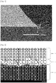
- Fig. 1 shows an enlarged photograph of a bonding cross section in one example of a ceramic circuit substrate according to the present embodiment.
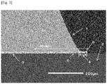
- This ceramic circuit substrate has a circuit pattern (copper circuit portion) 1 formed on a ceramic substrate (silicon nitride substrate) 2, with a braze material layer 7 interposed therebetween. A portion of the braze material layer 7 protrudes from the outer edge of the circuit pattern 1 and forms a protruding portion 4.
- the thickness of the braze material protrusion is 8 ⁇ m to 30 ⁇ m and the length thereof is 40 ⁇ m to 150 ⁇ m.
- the thickness of the braze material protrusion is 13 ⁇ m to 23 ⁇ m and the length of the protrusion is 50 ⁇ m to 100 ⁇ m.
- the length of the braze material protrusion is 150 ⁇ m or less, it is also possible to configure the outer dimensions of a substrate so as to be an acceptable size for design even given the recent market trends demanding products be made remarkably light, thin, short, and small.
- the braze material layer has Ag-rich phases which are formed continuously for 300 ⁇ m or more, and preferably 400 ⁇ m or more, towards the inside, from the outer edge of the protruding portion, along the bonding interface between the ceramic substrate and the circuit pattern 1.
- Ag-rich phases means phases formed from an Ag solid solution and predominantly comprises Ag.
- Predominantly means being 80% or more as a quantitative analysis using an electron probe micro-analyzer (EPMA).
- the Ag-rich phases contain Sn or In and Ti, and Cu may be included as a solid solution.
- phases observed as a white color when observed using a scanning electron microscope are referred to as "Ag-rich phases” and phases observed as a black color are referred to as "Cu-rich phases”.
- Al-rich phases formed continuously for 300 ⁇ m or more means that phases observed as a white color when observed using a scanning electron microscope are formed over 300 ⁇ m continuously (without any breaks) from the braze material protruding portion outer edge.
- the braze material layer 7 is configured from white-colored Ag-rich phases 3 and black-colored Cu-rich phases 6. Black-colored Cu-rich phases 6 may be included in the Ag-rich phases 3, but as long as the white-colored portion is not separated by any breaks, the meaning of "formed continuously” holds.
- the white-colored Ag-rich phases 3 are formed over at least 300 ⁇ m without any breaks therein.
- tiny black colors are observed in the white-colored Ag-rich phases, but the white-colored Ag-rich phases are formed continuously without being separated by any breaks.
- the white-colored Ag-rich phases are separated by a break at a location less than 100 ⁇ m from a braze material protruding portion outer edge 5, and a location configured from Cu-rich phases 6 alone appears (an Ag-rich phase broken portion).
- the Ag-rich phases 3 are formed continuously for 300 ⁇ m or more from the braze material protruding portion outer edge 5 and therefore, even under the harsher conditions of the thermal cycling tests, there is no breaking of the bonding interface between the Ag-rich phases and the Cu-rich phases near the braze material protruding portion (in a range of 300 ⁇ m or less from the protruding portion outer edge 5). As a result thereof, it is possible to configure a ceramic circuit substrate having excellent thermal cycling resistance properties.
- a circuit-forming metal plate was placed over one surface of the silicon nitride substrate and a heat dissipation plate-forming metal plate (both being C1020 oxygen-free copper plates having a thickness of 0.8 mm and a purity of 99.60%) was placed over the other surface, and these were bonded under conditions of 830°C for 30 minutes in a vacuum of 1.0 x 10 -3 Pa or lower.
- An etching resist was printed on the bonded copper plates and the copper plates were etched with a cupric chloride solution to form a circuit pattern.
- braze material layers and nitride layers were removed with an ammonium fluoride/hydrogen peroxide solution, and a protruding portion having a braze material protrusion length of 29 ⁇ m and a thickness of 5 ⁇ m was formed.
- a pre-treatment of degreasing and chemical polishing was performed and then an anti-corrosion treatment was carried out using a benzotriazole-based compound.
- the bonding void ratio of the ceramic circuit substrate was computed by measuring the area of bonding voids observed by an ultrasonic flaw detector (ES5000, manufactured by Hitachi Power Solutions Co., Ltd.) and dividing this value by the area of the copper circuit pattern.
- the bond structure of a cross section inside the circuit pattern from the braze material protruding portion outer edge in the ceramic circuit substrate was observed in reflected-electron images using a scanning electron microscope (SU6600, manufactured by Hitachi High-Technologies Corporation), with phases observed as a white color in the braze material layer being defined as Ag-rich phases, and phases observed as a black color being defined as Cu-rich phases.
- a scanning electron microscope (SU6600, manufactured by Hitachi High-Technologies Corporation)
- phases observed as a white color in the braze material layer being defined as Ag-rich phases
- phases observed as a black color being defined as Cu-rich phases.
- the continuity of the Ag-rich phases was confirmed by observing the inside of the circuit pattern from the braze material protruding portion outer edge in four fields of view at a 200-times magnification, the fields or view being 400 ⁇ m long and 600 ⁇ m wide.
- the braze material protruding portion in a cross section of a circuit pattern corner section in the ceramic circuit substrate was observed in reflected-electron images using a scanning electron microscope (SU6600, manufactured by Hitachi High-Technologies Corporation) in five fields of view at a 200-times magnification, the fields of view being 400 ⁇ m long and 600 ⁇ m wide.
- a scanning electron microscope SU6600, manufactured by Hitachi High-Technologies Corporation
- an average of the maximum thickness and the minimum thickness for each field of view was determined, and the average value of the five fields of view was deemed to be the thickness of the braze material layer.
- a distance between the copper circuit pattern outer edge and the braze material protruding portion outer edge was determined for each field of view, and the average value of the five fields of view was deemed to be the length of the braze material layer.
- a fabricated ceramic circuit substrate was repeatedly tested over 2,500 cycles in thermal cycling resistance tests wherein each cycle involved setting the temperature so as to change between -55 °C for 15 minutes, 25 °C for 15 minutes, 175°C for 15 minutes, and 25 °C for 15 minutes. Thereafter, the metal plate and the braze material layer were stripped with iron chloride and an ammonium fluoride/hydrogen peroxide etching solution, and the area of cracks generated at the surface of the ceramic substrate was computed by using a scanner to input an image at a resolution of 600 dpi ⁇ 600 dpi, using the image analysis software GIMP2 (threshold value 140) to digitize the image, and then computing the crack area. This was divided by the copper circuit pattern area to determine the crack ratio.
- Ceramic circuit substrates were obtained in the same manner as Example 1 with the exception that Sn powder was not used in the braze material used for bonding, the braze material blend and bonding conditions shown in Table 2 were set, and the length and thickness of the protruding portion were set as in Table 4. The various kinds of measurements and evaluations were also carried out in the same manner as in Example 1. The results are shown in Table 4.
- Ceramic circuit substrates were obtained in the same manner as in Example 5 with the exception that the braze material blend and bonding conditions shown in Table 2 were used, and the length and thickness of the protruding portion were set as in Table 4. The various kinds of measurements and evaluations were also carried out in the same manner as in Example 5. The results are shown in Table 4.
- Ceramic circuit substrates were obtained in the same manner as in Example 5 with the exception that the braze material blend and bonding conditions shown in Table 2 were used, and the length and thickness of the protruding portion were set as in Table 4. The various kinds of measurements and evaluations were also carried out in the same manner as in Example 5. The results are shown in Table 4.
- Ceramic circuit substrates were obtained in the same manner as in Example 5 with the exception that the braze material blend and bonding conditions shown in Table 2 were used, and the length and thickness of the protruding portion were set as in Table 4. The various kinds of measurements and evaluations were also carried out in the same manner as in Example 5. The results are shown in Table 4.
- Ceramic circuit substrates were obtained in the same manner as in Example 1 with the exception that the braze material blend and bonding conditions shown in Table 2 were used, and the length and thickness of the protruding portion were set as in Table 4. The various kinds of measurements and evaluations were also carried out in the same manner as in Example 1. The results are shown in Table 4.
- Example 1 Braze material blend Bonding conditions Ag (parts by mass) Cu (parts by mass) Sn (parts by mass) In (parts by mass) TiH 2 (parts by mass) Bonding temperature (°C) Retention time (minutes)
- Example 1 89.5 9.5 1.0 - 3.5 830 30
- Example 2 88.5 9.5 2.0 - 3.5 830 30
- Example 3 89.5 9.5 1.0 - 3.5 860 30
- Example 4 89.5 9.5 1.0 - 3.5 830 30
- Example 5 89.0 9.5 - 1.5 3.5 825 30
- Example 6 89.5 9.5 1.0 - 3.5 830 30
- Example 7 89.5 9.5 1.0 - 3.5 830 30
- Example 8 89.5 9.5 1.0 - 3.5 830 30
- Example 9 93.0 5.5 1.5 - 3.5 810 40
- Example 10 85.0 13.0 2.0 - 3.5 800 30
- Example 11 85.0 13.0 - 2.0 3.5 800 30
- Example 12 89.5 9.5
- the Ag-rich phases were continuous for 300 ⁇ m or more, towards the inside of the circuit pattern, from the outer edge of the protruding portion formed by the braze material layer, and the crack ratio after thermal cycling tests was 2.0% or less.
- the crack ratio becomes 1.5% or less, and by satisfying both of the foregoing conditions, the crack ratio becomes 1.0% or less.
Landscapes
- Engineering & Computer Science (AREA)
- Chemical & Material Sciences (AREA)
- Mechanical Engineering (AREA)
- Materials Engineering (AREA)
- Microelectronics & Electronic Packaging (AREA)
- Ceramic Engineering (AREA)
- Organic Chemistry (AREA)
- Inorganic Chemistry (AREA)
- Manufacturing & Machinery (AREA)
- Metallurgy (AREA)
- Structural Engineering (AREA)
- Manufacturing Of Printed Wiring (AREA)
- Ceramic Products (AREA)
- Parts Printed On Printed Circuit Boards (AREA)
Applications Claiming Priority (2)
| Application Number | Priority Date | Filing Date | Title |
|---|---|---|---|
| JP2017143417 | 2017-07-25 | ||
| PCT/JP2018/027882 WO2019022133A1 (fr) | 2017-07-25 | 2018-07-25 | Carte de circuit imprimé en céramique et son procédé de production |
Publications (3)
| Publication Number | Publication Date |
|---|---|
| EP3661337A1 true EP3661337A1 (fr) | 2020-06-03 |
| EP3661337A4 EP3661337A4 (fr) | 2020-07-22 |
| EP3661337B1 EP3661337B1 (fr) | 2021-09-01 |
Family
ID=65041218
Family Applications (1)
| Application Number | Title | Priority Date | Filing Date |
|---|---|---|---|
| EP18839092.6A Active EP3661337B1 (fr) | 2017-07-25 | 2018-07-25 | Carte de circuit imprimé en céramique et son procédé de production |
Country Status (6)
| Country | Link |
|---|---|
| US (1) | US11483926B2 (fr) |
| EP (1) | EP3661337B1 (fr) |
| JP (1) | JP7010950B2 (fr) |
| KR (1) | KR102521140B1 (fr) |
| CN (1) | CN110945974B (fr) |
| WO (1) | WO2019022133A1 (fr) |
Cited By (5)
| Publication number | Priority date | Publication date | Assignee | Title |
|---|---|---|---|---|
| CN111958145A (zh) * | 2020-08-24 | 2020-11-20 | 合肥工业大学 | 一种用于max相复合陶瓷的钎焊材料及钎焊工艺 |
| EP4311818A1 (fr) * | 2022-07-29 | 2024-01-31 | Heraeus Electronics GmbH & Co. KG | Substrat métallique céramique pourvu de zone de contact |
| EP4311819A1 (fr) * | 2022-07-29 | 2024-01-31 | Heraeus Electronics GmbH & Co. KG | Substrat métallique céramique pourvu de zone de contact |
| EP4593076A1 (fr) * | 2024-01-24 | 2025-07-30 | Heraeus Electronics GmbH & Co. KG | Substrat métal-céramique avec zone de contact |
| EP4593075A1 (fr) * | 2024-01-24 | 2025-07-30 | Heraeus Electronics GmbH & Co. KG | Substrat métal-céramique avec zone de contact |
Families Citing this family (13)
| Publication number | Priority date | Publication date | Assignee | Title |
|---|---|---|---|---|
| KR20220066051A (ko) * | 2019-09-20 | 2022-05-23 | 덴카 주식회사 | 회로 기판 및 이것을 구비하는 모듈 |
| WO2021149789A1 (fr) * | 2020-01-23 | 2021-07-29 | デンカ株式会社 | Composite céramique-cuivre et procédé de production d'un composite céramique-cuivre |
| CN115136297A (zh) * | 2020-02-13 | 2022-09-30 | 阿莫绿色技术有限公司 | 功率模块及其制造方法 |
| CN119501220A (zh) * | 2020-02-17 | 2025-02-25 | 株式会社东芝 | 接合体的制造方法 |
| CN114929650A (zh) | 2020-03-30 | 2022-08-19 | 电化株式会社 | 电路基板、接合体以及它们的制造方法 |
| JP7717699B6 (ja) * | 2020-07-27 | 2025-08-27 | 株式会社東芝 | 接合体、回路基板、半導体装置、及び接合体の製造方法 |
| EP4197990A4 (fr) * | 2020-08-12 | 2024-08-07 | Tokuyama Corporation | Stratifié pour carte de circuit imprimé |
| EP4234517B1 (fr) * | 2020-10-20 | 2025-10-01 | Kabushiki Kaisha Toshiba | Corps assemblé, carte de circuit imprimé en céramique l'utilisant, et dispositif semi-conducteur |
| CN112469201B (zh) * | 2020-11-24 | 2021-12-07 | 绍兴德汇半导体材料有限公司 | 一种覆铜衬板制作方法 |
| EP4270499A4 (fr) * | 2020-12-25 | 2025-01-29 | CoorsTek GK | Élément de silice et dispositif à del |
| CN116964022A (zh) * | 2021-03-24 | 2023-10-27 | 电化株式会社 | 复合基板 |
| CN119547568A (zh) * | 2022-05-19 | 2025-02-28 | 阿尔法能源技术公司 | 将锂耦合到衬底 |
| JP7576209B2 (ja) * | 2022-11-25 | 2024-10-30 | デンカ株式会社 | 窒化ケイ素焼結体及びその製造方法、接合体、並びに、パワーモジュール |
Family Cites Families (14)
| Publication number | Priority date | Publication date | Assignee | Title |
|---|---|---|---|---|
| EP0480470B1 (fr) * | 1990-10-12 | 1995-03-29 | Sumitomo Electric Industries, Ltd. | Elément isolant et parties électriques utilisant celui-ci |
| JP3449458B2 (ja) * | 1997-05-26 | 2003-09-22 | 電気化学工業株式会社 | 回路基板 |
| JP4168114B2 (ja) | 2001-09-28 | 2008-10-22 | Dowaホールディングス株式会社 | 金属−セラミックス接合体 |
| CN100471668C (zh) * | 2002-11-20 | 2009-03-25 | 同和控股(集团)有限公司 | 金属/陶瓷粘合制品 |
| JP4394477B2 (ja) | 2003-03-27 | 2010-01-06 | Dowaホールディングス株式会社 | 金属−セラミックス接合基板の製造方法 |
| JP5299160B2 (ja) * | 2003-03-27 | 2013-09-25 | Dowaメタルテック株式会社 | 金属−セラミックス接合基板の製造方法 |
| JP4345054B2 (ja) * | 2003-10-09 | 2009-10-14 | 日立金属株式会社 | セラミックス基板用ろう材及びこれを用いたセラミックス回路基板、パワー半導体モジュール |
| CN100428432C (zh) * | 2004-03-24 | 2008-10-22 | 德山株式会社 | 元件接合用基板及其制造方法 |
| JP4345066B2 (ja) | 2005-05-24 | 2009-10-14 | 日立金属株式会社 | セラミックス回路基板及びこれを用いたパワー半導体モジュール |
| EP3273755B1 (fr) | 2009-09-15 | 2018-11-07 | Kabushiki Kaisha Toshiba | Procédé de fabrication d'une carte de circuit céramique |
| JP5725178B2 (ja) * | 2011-06-30 | 2015-05-27 | 日立金属株式会社 | ろう材、ろう材ペースト、セラミックス回路基板、セラミックスマスター回路基板及びパワー半導体モジュール |
| EP3125286B1 (fr) | 2014-03-26 | 2019-05-08 | Kyocera Corporation | Carte de circuit imprimé et dispositif électrique la comportant |
| US9872380B2 (en) * | 2014-07-29 | 2018-01-16 | Denka Company Limited | Ceramic circuit board and method for producing same |
| EP3358614B1 (fr) | 2015-09-28 | 2022-12-14 | Kabushiki Kaisha Toshiba | Substrat de circuit et dispositif à semi-conducteur |
-
2018
- 2018-07-25 WO PCT/JP2018/027882 patent/WO2019022133A1/fr not_active Ceased
- 2018-07-25 KR KR1020207001838A patent/KR102521140B1/ko active Active
- 2018-07-25 JP JP2019532831A patent/JP7010950B2/ja active Active
- 2018-07-25 CN CN201880048695.7A patent/CN110945974B/zh active Active
- 2018-07-25 US US16/630,232 patent/US11483926B2/en active Active
- 2018-07-25 EP EP18839092.6A patent/EP3661337B1/fr active Active
Cited By (7)
| Publication number | Priority date | Publication date | Assignee | Title |
|---|---|---|---|---|
| CN111958145A (zh) * | 2020-08-24 | 2020-11-20 | 合肥工业大学 | 一种用于max相复合陶瓷的钎焊材料及钎焊工艺 |
| EP4311818A1 (fr) * | 2022-07-29 | 2024-01-31 | Heraeus Electronics GmbH & Co. KG | Substrat métallique céramique pourvu de zone de contact |
| EP4311819A1 (fr) * | 2022-07-29 | 2024-01-31 | Heraeus Electronics GmbH & Co. KG | Substrat métallique céramique pourvu de zone de contact |
| WO2024022743A1 (fr) * | 2022-07-29 | 2024-02-01 | Heraeus Electronics Gmbh & Co. Kg | Substrat métal-céramique avec zone de contact |
| WO2024022742A1 (fr) * | 2022-07-29 | 2024-02-01 | Heraeus Electronics Gmbh & Co. Kg | Substrat métal-céramique avec zone de contact |
| EP4593076A1 (fr) * | 2024-01-24 | 2025-07-30 | Heraeus Electronics GmbH & Co. KG | Substrat métal-céramique avec zone de contact |
| EP4593075A1 (fr) * | 2024-01-24 | 2025-07-30 | Heraeus Electronics GmbH & Co. KG | Substrat métal-céramique avec zone de contact |
Also Published As
| Publication number | Publication date |
|---|---|
| US11483926B2 (en) | 2022-10-25 |
| KR102521140B1 (ko) | 2023-04-12 |
| EP3661337B1 (fr) | 2021-09-01 |
| WO2019022133A1 (fr) | 2019-01-31 |
| EP3661337A4 (fr) | 2020-07-22 |
| CN110945974B (zh) | 2023-05-16 |
| CN110945974A (zh) | 2020-03-31 |
| JPWO2019022133A1 (ja) | 2020-06-11 |
| US20200163210A1 (en) | 2020-05-21 |
| KR20200029480A (ko) | 2020-03-18 |
| JP7010950B2 (ja) | 2022-01-26 |
Similar Documents
| Publication | Publication Date | Title |
|---|---|---|
| EP3661337B1 (fr) | Carte de circuit imprimé en céramique et son procédé de production | |
| EP3632879B1 (fr) | Carte de circuit imprimé en céramique et son procede de fabrication | |
| US9780011B2 (en) | Brazing material, brazing material paste, ceramic circuit substrate, ceramic master circuit substrate, and power semiconductor module | |
| EP3632880B1 (fr) | Carte de circuit imprimé en céramique et procédé pour sa production | |
| JP6244405B2 (ja) | 配線パターンを形成するための組成物 | |
| JP5492191B2 (ja) | メタライズド基板を製造する方法、メタライズド基板 | |
| CN113632217A (zh) | 氮化硅基板、氮化硅-金属复合体、氮化硅电路基板及半导体封装件 | |
| JP3629783B2 (ja) | 回路基板 | |
| CN114080868A (zh) | 通孔填充基板的制造方法以及导电糊的套装 | |
| US20040023011A1 (en) | Copper paste, wiring board using the same, and production method of wiring board | |
| JP5201974B2 (ja) | メタライズド基板の製造方法 |
Legal Events
| Date | Code | Title | Description |
|---|---|---|---|
| STAA | Information on the status of an ep patent application or granted ep patent |
Free format text: STATUS: THE INTERNATIONAL PUBLICATION HAS BEEN MADE |
|
| PUAI | Public reference made under article 153(3) epc to a published international application that has entered the european phase |
Free format text: ORIGINAL CODE: 0009012 |
|
| STAA | Information on the status of an ep patent application or granted ep patent |
Free format text: STATUS: REQUEST FOR EXAMINATION WAS MADE |
|
| 17P | Request for examination filed |
Effective date: 20200205 |
|
| AK | Designated contracting states |
Kind code of ref document: A1 Designated state(s): AL AT BE BG CH CY CZ DE DK EE ES FI FR GB GR HR HU IE IS IT LI LT LU LV MC MK MT NL NO PL PT RO RS SE SI SK SM TR |
|
| AX | Request for extension of the european patent |
Extension state: BA ME |
|
| A4 | Supplementary search report drawn up and despatched |
Effective date: 20200622 |
|
| RIC1 | Information provided on ipc code assigned before grant |
Ipc: B23K 1/19 20060101ALI20200616BHEP Ipc: H05K 1/09 20060101ALN20200616BHEP Ipc: H05K 3/06 20060101ALN20200616BHEP Ipc: H01L 23/13 20060101ALI20200616BHEP Ipc: H05K 3/28 20060101ALN20200616BHEP Ipc: H05K 3/24 20060101ALN20200616BHEP Ipc: B23K 1/00 20060101ALI20200616BHEP Ipc: C22C 5/06 20060101ALI20200616BHEP Ipc: H05K 3/02 20060101ALN20200616BHEP Ipc: B23K 35/30 20060101ALI20200616BHEP Ipc: H05K 1/03 20060101ALN20200616BHEP Ipc: H01L 23/373 20060101ALI20200616BHEP Ipc: H05K 3/38 20060101AFI20200616BHEP Ipc: H01L 23/15 20060101ALI20200616BHEP Ipc: C04B 37/02 20060101ALI20200616BHEP Ipc: H05K 3/26 20060101ALN20200616BHEP |
|
| DAV | Request for validation of the european patent (deleted) | ||
| DAX | Request for extension of the european patent (deleted) | ||
| REG | Reference to a national code |
Ref country code: DE Ref legal event code: R079 Ref document number: 602018023059 Country of ref document: DE Free format text: PREVIOUS MAIN CLASS: H05K0001090000 Ipc: H05K0003380000 |
|
| GRAP | Despatch of communication of intention to grant a patent |
Free format text: ORIGINAL CODE: EPIDOSNIGR1 |
|
| STAA | Information on the status of an ep patent application or granted ep patent |
Free format text: STATUS: GRANT OF PATENT IS INTENDED |
|
| RIC1 | Information provided on ipc code assigned before grant |
Ipc: B23K 35/02 20060101ALN20210306BHEP Ipc: H05K 3/28 20060101ALN20210306BHEP Ipc: H05K 3/26 20060101ALN20210306BHEP Ipc: H05K 3/24 20060101ALN20210306BHEP Ipc: H05K 3/06 20060101ALN20210306BHEP Ipc: H05K 3/02 20060101ALN20210306BHEP Ipc: H05K 1/09 20060101ALN20210306BHEP Ipc: H05K 1/03 20060101ALN20210306BHEP Ipc: C22C 5/08 20060101ALI20210306BHEP Ipc: H01L 23/373 20060101ALI20210306BHEP Ipc: H01L 23/15 20060101ALI20210306BHEP Ipc: C04B 37/02 20060101ALI20210306BHEP Ipc: H01L 23/13 20060101ALI20210306BHEP Ipc: C22C 5/06 20060101ALI20210306BHEP Ipc: B23K 35/30 20060101ALI20210306BHEP Ipc: B23K 1/19 20060101ALI20210306BHEP Ipc: B23K 1/00 20060101ALI20210306BHEP Ipc: H05K 3/38 20060101AFI20210306BHEP |
|
| INTG | Intention to grant announced |
Effective date: 20210322 |
|
| GRAS | Grant fee paid |
Free format text: ORIGINAL CODE: EPIDOSNIGR3 |
|
| GRAA | (expected) grant |
Free format text: ORIGINAL CODE: 0009210 |
|
| STAA | Information on the status of an ep patent application or granted ep patent |
Free format text: STATUS: THE PATENT HAS BEEN GRANTED |
|
| AK | Designated contracting states |
Kind code of ref document: B1 Designated state(s): AL AT BE BG CH CY CZ DE DK EE ES FI FR GB GR HR HU IE IS IT LI LT LU LV MC MK MT NL NO PL PT RO RS SE SI SK SM TR |
|
| REG | Reference to a national code |
Ref country code: GB Ref legal event code: FG4D |
|
| REG | Reference to a national code |
Ref country code: CH Ref legal event code: EP Ref country code: AT Ref legal event code: REF Ref document number: 1427660 Country of ref document: AT Kind code of ref document: T Effective date: 20210915 |
|
| REG | Reference to a national code |
Ref country code: DE Ref legal event code: R096 Ref document number: 602018023059 Country of ref document: DE |
|
| REG | Reference to a national code |
Ref country code: IE Ref legal event code: FG4D |
|
| REG | Reference to a national code |
Ref country code: LT Ref legal event code: MG9D |
|
| REG | Reference to a national code |
Ref country code: NL Ref legal event code: MP Effective date: 20210901 |
|
| PG25 | Lapsed in a contracting state [announced via postgrant information from national office to epo] |
Ref country code: BG Free format text: LAPSE BECAUSE OF FAILURE TO SUBMIT A TRANSLATION OF THE DESCRIPTION OR TO PAY THE FEE WITHIN THE PRESCRIBED TIME-LIMIT Effective date: 20211201 Ref country code: LT Free format text: LAPSE BECAUSE OF FAILURE TO SUBMIT A TRANSLATION OF THE DESCRIPTION OR TO PAY THE FEE WITHIN THE PRESCRIBED TIME-LIMIT Effective date: 20210901 Ref country code: NO Free format text: LAPSE BECAUSE OF FAILURE TO SUBMIT A TRANSLATION OF THE DESCRIPTION OR TO PAY THE FEE WITHIN THE PRESCRIBED TIME-LIMIT Effective date: 20211201 Ref country code: HR Free format text: LAPSE BECAUSE OF FAILURE TO SUBMIT A TRANSLATION OF THE DESCRIPTION OR TO PAY THE FEE WITHIN THE PRESCRIBED TIME-LIMIT Effective date: 20210901 Ref country code: RS Free format text: LAPSE BECAUSE OF FAILURE TO SUBMIT A TRANSLATION OF THE DESCRIPTION OR TO PAY THE FEE WITHIN THE PRESCRIBED TIME-LIMIT Effective date: 20210901 Ref country code: SE Free format text: LAPSE BECAUSE OF FAILURE TO SUBMIT A TRANSLATION OF THE DESCRIPTION OR TO PAY THE FEE WITHIN THE PRESCRIBED TIME-LIMIT Effective date: 20210901 Ref country code: FI Free format text: LAPSE BECAUSE OF FAILURE TO SUBMIT A TRANSLATION OF THE DESCRIPTION OR TO PAY THE FEE WITHIN THE PRESCRIBED TIME-LIMIT Effective date: 20210901 Ref country code: ES Free format text: LAPSE BECAUSE OF FAILURE TO SUBMIT A TRANSLATION OF THE DESCRIPTION OR TO PAY THE FEE WITHIN THE PRESCRIBED TIME-LIMIT Effective date: 20210901 |
|
| REG | Reference to a national code |
Ref country code: AT Ref legal event code: MK05 Ref document number: 1427660 Country of ref document: AT Kind code of ref document: T Effective date: 20210901 |
|
| PG25 | Lapsed in a contracting state [announced via postgrant information from national office to epo] |
Ref country code: PL Free format text: LAPSE BECAUSE OF FAILURE TO SUBMIT A TRANSLATION OF THE DESCRIPTION OR TO PAY THE FEE WITHIN THE PRESCRIBED TIME-LIMIT Effective date: 20210901 Ref country code: LV Free format text: LAPSE BECAUSE OF FAILURE TO SUBMIT A TRANSLATION OF THE DESCRIPTION OR TO PAY THE FEE WITHIN THE PRESCRIBED TIME-LIMIT Effective date: 20210901 Ref country code: GR Free format text: LAPSE BECAUSE OF FAILURE TO SUBMIT A TRANSLATION OF THE DESCRIPTION OR TO PAY THE FEE WITHIN THE PRESCRIBED TIME-LIMIT Effective date: 20211202 |
|
| PG25 | Lapsed in a contracting state [announced via postgrant information from national office to epo] |
Ref country code: AT Free format text: LAPSE BECAUSE OF FAILURE TO SUBMIT A TRANSLATION OF THE DESCRIPTION OR TO PAY THE FEE WITHIN THE PRESCRIBED TIME-LIMIT Effective date: 20210901 |
|
| PG25 | Lapsed in a contracting state [announced via postgrant information from national office to epo] |
Ref country code: IS Free format text: LAPSE BECAUSE OF FAILURE TO SUBMIT A TRANSLATION OF THE DESCRIPTION OR TO PAY THE FEE WITHIN THE PRESCRIBED TIME-LIMIT Effective date: 20220101 Ref country code: SM Free format text: LAPSE BECAUSE OF FAILURE TO SUBMIT A TRANSLATION OF THE DESCRIPTION OR TO PAY THE FEE WITHIN THE PRESCRIBED TIME-LIMIT Effective date: 20210901 Ref country code: SK Free format text: LAPSE BECAUSE OF FAILURE TO SUBMIT A TRANSLATION OF THE DESCRIPTION OR TO PAY THE FEE WITHIN THE PRESCRIBED TIME-LIMIT Effective date: 20210901 Ref country code: RO Free format text: LAPSE BECAUSE OF FAILURE TO SUBMIT A TRANSLATION OF THE DESCRIPTION OR TO PAY THE FEE WITHIN THE PRESCRIBED TIME-LIMIT Effective date: 20210901 Ref country code: PT Free format text: LAPSE BECAUSE OF FAILURE TO SUBMIT A TRANSLATION OF THE DESCRIPTION OR TO PAY THE FEE WITHIN THE PRESCRIBED TIME-LIMIT Effective date: 20220103 Ref country code: NL Free format text: LAPSE BECAUSE OF FAILURE TO SUBMIT A TRANSLATION OF THE DESCRIPTION OR TO PAY THE FEE WITHIN THE PRESCRIBED TIME-LIMIT Effective date: 20210901 Ref country code: EE Free format text: LAPSE BECAUSE OF FAILURE TO SUBMIT A TRANSLATION OF THE DESCRIPTION OR TO PAY THE FEE WITHIN THE PRESCRIBED TIME-LIMIT Effective date: 20210901 Ref country code: CZ Free format text: LAPSE BECAUSE OF FAILURE TO SUBMIT A TRANSLATION OF THE DESCRIPTION OR TO PAY THE FEE WITHIN THE PRESCRIBED TIME-LIMIT Effective date: 20210901 Ref country code: AL Free format text: LAPSE BECAUSE OF FAILURE TO SUBMIT A TRANSLATION OF THE DESCRIPTION OR TO PAY THE FEE WITHIN THE PRESCRIBED TIME-LIMIT Effective date: 20210901 |
|
| REG | Reference to a national code |
Ref country code: DE Ref legal event code: R097 Ref document number: 602018023059 Country of ref document: DE |
|
| PLBE | No opposition filed within time limit |
Free format text: ORIGINAL CODE: 0009261 |
|
| STAA | Information on the status of an ep patent application or granted ep patent |
Free format text: STATUS: NO OPPOSITION FILED WITHIN TIME LIMIT |
|
| PG25 | Lapsed in a contracting state [announced via postgrant information from national office to epo] |
Ref country code: DK Free format text: LAPSE BECAUSE OF FAILURE TO SUBMIT A TRANSLATION OF THE DESCRIPTION OR TO PAY THE FEE WITHIN THE PRESCRIBED TIME-LIMIT Effective date: 20210901 |
|
| 26N | No opposition filed |
Effective date: 20220602 |
|
| PG25 | Lapsed in a contracting state [announced via postgrant information from national office to epo] |
Ref country code: SI Free format text: LAPSE BECAUSE OF FAILURE TO SUBMIT A TRANSLATION OF THE DESCRIPTION OR TO PAY THE FEE WITHIN THE PRESCRIBED TIME-LIMIT Effective date: 20210901 |
|
| PG25 | Lapsed in a contracting state [announced via postgrant information from national office to epo] |
Ref country code: MC Free format text: LAPSE BECAUSE OF FAILURE TO SUBMIT A TRANSLATION OF THE DESCRIPTION OR TO PAY THE FEE WITHIN THE PRESCRIBED TIME-LIMIT Effective date: 20210901 |
|
| REG | Reference to a national code |
Ref country code: BE Ref legal event code: MM Effective date: 20220731 |
|
| PG25 | Lapsed in a contracting state [announced via postgrant information from national office to epo] |
Ref country code: LU Free format text: LAPSE BECAUSE OF NON-PAYMENT OF DUE FEES Effective date: 20220725 |
|
| PG25 | Lapsed in a contracting state [announced via postgrant information from national office to epo] |
Ref country code: BE Free format text: LAPSE BECAUSE OF NON-PAYMENT OF DUE FEES Effective date: 20220731 |
|
| P01 | Opt-out of the competence of the unified patent court (upc) registered |
Effective date: 20230512 |
|
| PG25 | Lapsed in a contracting state [announced via postgrant information from national office to epo] |
Ref country code: IE Free format text: LAPSE BECAUSE OF NON-PAYMENT OF DUE FEES Effective date: 20220725 |
|
| PG25 | Lapsed in a contracting state [announced via postgrant information from national office to epo] |
Ref country code: MK Free format text: LAPSE BECAUSE OF FAILURE TO SUBMIT A TRANSLATION OF THE DESCRIPTION OR TO PAY THE FEE WITHIN THE PRESCRIBED TIME-LIMIT Effective date: 20210901 Ref country code: CY Free format text: LAPSE BECAUSE OF FAILURE TO SUBMIT A TRANSLATION OF THE DESCRIPTION OR TO PAY THE FEE WITHIN THE PRESCRIBED TIME-LIMIT Effective date: 20210901 |
|
| PG25 | Lapsed in a contracting state [announced via postgrant information from national office to epo] |
Ref country code: HU Free format text: LAPSE BECAUSE OF FAILURE TO SUBMIT A TRANSLATION OF THE DESCRIPTION OR TO PAY THE FEE WITHIN THE PRESCRIBED TIME-LIMIT; INVALID AB INITIO Effective date: 20180725 |
|
| PG25 | Lapsed in a contracting state [announced via postgrant information from national office to epo] |
Ref country code: TR Free format text: LAPSE BECAUSE OF FAILURE TO SUBMIT A TRANSLATION OF THE DESCRIPTION OR TO PAY THE FEE WITHIN THE PRESCRIBED TIME-LIMIT Effective date: 20210901 |
|
| PGFP | Annual fee paid to national office [announced via postgrant information from national office to epo] |
Ref country code: GB Payment date: 20240606 Year of fee payment: 7 |
|
| PGFP | Annual fee paid to national office [announced via postgrant information from national office to epo] |
Ref country code: FR Payment date: 20240611 Year of fee payment: 7 |
|
| PG25 | Lapsed in a contracting state [announced via postgrant information from national office to epo] |
Ref country code: MT Free format text: LAPSE BECAUSE OF FAILURE TO SUBMIT A TRANSLATION OF THE DESCRIPTION OR TO PAY THE FEE WITHIN THE PRESCRIBED TIME-LIMIT Effective date: 20210901 |
|
| PGFP | Annual fee paid to national office [announced via postgrant information from national office to epo] |
Ref country code: IT Payment date: 20240612 Year of fee payment: 7 |
|
| PGFP | Annual fee paid to national office [announced via postgrant information from national office to epo] |
Ref country code: DE Payment date: 20240529 Year of fee payment: 7 |
|
| PGFP | Annual fee paid to national office [announced via postgrant information from national office to epo] |
Ref country code: CH Payment date: 20240801 Year of fee payment: 7 |
|
| REG | Reference to a national code |
Ref country code: DE Ref legal event code: R119 Ref document number: 602018023059 Country of ref document: DE |
|
| REG | Reference to a national code |
Ref country code: CH Ref legal event code: H13 Free format text: ST27 STATUS EVENT CODE: U-0-0-H10-H13 (AS PROVIDED BY THE NATIONAL OFFICE) Effective date: 20260224 |
|
| GBPC | Gb: european patent ceased through non-payment of renewal fee |
Effective date: 20250725 |
|
| PG25 | Lapsed in a contracting state [announced via postgrant information from national office to epo] |
Ref country code: GB Free format text: LAPSE BECAUSE OF NON-PAYMENT OF DUE FEES Effective date: 20250725 |
|
| PG25 | Lapsed in a contracting state [announced via postgrant information from national office to epo] |
Ref country code: DE Free format text: LAPSE BECAUSE OF NON-PAYMENT OF DUE FEES Effective date: 20260203 |
|
| PG25 | Lapsed in a contracting state [announced via postgrant information from national office to epo] |
Ref country code: FR Free format text: LAPSE BECAUSE OF NON-PAYMENT OF DUE FEES Effective date: 20250731 |
|
| PG25 | Lapsed in a contracting state [announced via postgrant information from national office to epo] |
Ref country code: CH Free format text: LAPSE BECAUSE OF NON-PAYMENT OF DUE FEES Effective date: 20250731 |