EP3663746A1 - Détecteur de substances étrangères de surface pour film transparent ou translucide - Google Patents
Détecteur de substances étrangères de surface pour film transparent ou translucide Download PDFInfo
- Publication number
- EP3663746A1 EP3663746A1 EP18840625.0A EP18840625A EP3663746A1 EP 3663746 A1 EP3663746 A1 EP 3663746A1 EP 18840625 A EP18840625 A EP 18840625A EP 3663746 A1 EP3663746 A1 EP 3663746A1
- Authority
- EP
- European Patent Office
- Prior art keywords
- film
- light
- foreign substance
- holder
- light emission
- Prior art date
- Legal status (The legal status is an assumption and is not a legal conclusion. Google has not performed a legal analysis and makes no representation as to the accuracy of the status listed.)
- Granted
Links
Images



Classifications
-
- G—PHYSICS
- G01—MEASURING; TESTING
- G01N—INVESTIGATING OR ANALYSING MATERIALS BY DETERMINING THEIR CHEMICAL OR PHYSICAL PROPERTIES
- G01N21/00—Investigating or analysing materials by the use of optical means, i.e. using sub-millimetre waves, infrared, visible or ultraviolet light
- G01N21/84—Systems specially adapted for particular applications
- G01N21/88—Investigating the presence of flaws or contamination
- G01N21/8806—Specially adapted optical and illumination features
-
- G—PHYSICS
- G01—MEASURING; TESTING
- G01N—INVESTIGATING OR ANALYSING MATERIALS BY DETERMINING THEIR CHEMICAL OR PHYSICAL PROPERTIES
- G01N21/00—Investigating or analysing materials by the use of optical means, i.e. using sub-millimetre waves, infrared, visible or ultraviolet light
- G01N21/84—Systems specially adapted for particular applications
- G01N21/88—Investigating the presence of flaws or contamination
- G01N21/94—Investigating contamination, e.g. dust
-
- B—PERFORMING OPERATIONS; TRANSPORTING
- B03—SEPARATION OF SOLID MATERIALS USING LIQUIDS OR USING PNEUMATIC TABLES OR JIGS; MAGNETIC OR ELECTROSTATIC SEPARATION OF SOLID MATERIALS FROM SOLID MATERIALS OR FLUIDS; SEPARATION BY HIGH-VOLTAGE ELECTRIC FIELDS
- B03C—MAGNETIC OR ELECTROSTATIC SEPARATION OF SOLID MATERIALS FROM SOLID MATERIALS OR FLUIDS; SEPARATION BY HIGH-VOLTAGE ELECTRIC FIELDS
- B03C3/00—Separating dispersed particles from gases or vapour, e.g. air, by electrostatic effect
- B03C3/017—Combinations of electrostatic separation with other processes, not otherwise provided for
-
- G—PHYSICS
- G01—MEASURING; TESTING
- G01N—INVESTIGATING OR ANALYSING MATERIALS BY DETERMINING THEIR CHEMICAL OR PHYSICAL PROPERTIES
- G01N15/00—Investigating characteristics of particles; Investigating permeability, pore-volume or surface-area of porous materials
- G01N15/06—Investigating concentration of particle suspensions
- G01N15/0606—Investigating concentration of particle suspensions by collecting particles on a support
- G01N15/0612—Optical scan of the deposits
-
- G—PHYSICS
- G01—MEASURING; TESTING
- G01N—INVESTIGATING OR ANALYSING MATERIALS BY DETERMINING THEIR CHEMICAL OR PHYSICAL PROPERTIES
- G01N21/00—Investigating or analysing materials by the use of optical means, i.e. using sub-millimetre waves, infrared, visible or ultraviolet light
- G01N21/84—Systems specially adapted for particular applications
- G01N21/88—Investigating the presence of flaws or contamination
- G01N21/8851—Scan or image signal processing specially adapted therefor, e.g. for scan signal adjustment, for detecting different kinds of defects, for compensating for structures, markings, edges
-
- G—PHYSICS
- G01—MEASURING; TESTING
- G01N—INVESTIGATING OR ANALYSING MATERIALS BY DETERMINING THEIR CHEMICAL OR PHYSICAL PROPERTIES
- G01N21/00—Investigating or analysing materials by the use of optical means, i.e. using sub-millimetre waves, infrared, visible or ultraviolet light
- G01N21/84—Systems specially adapted for particular applications
- G01N21/88—Investigating the presence of flaws or contamination
- G01N21/95—Investigating the presence of flaws or contamination characterised by the material or shape of the object to be examined
- G01N21/956—Inspecting patterns on the surface of objects
-
- G—PHYSICS
- G01—MEASURING; TESTING
- G01N—INVESTIGATING OR ANALYSING MATERIALS BY DETERMINING THEIR CHEMICAL OR PHYSICAL PROPERTIES
- G01N21/00—Investigating or analysing materials by the use of optical means, i.e. using sub-millimetre waves, infrared, visible or ultraviolet light
- G01N21/84—Systems specially adapted for particular applications
- G01N21/88—Investigating the presence of flaws or contamination
- G01N21/95—Investigating the presence of flaws or contamination characterised by the material or shape of the object to be examined
- G01N21/958—Inspecting transparent materials or objects, e.g. windscreens
-
- G—PHYSICS
- G02—OPTICS
- G02F—OPTICAL DEVICES OR ARRANGEMENTS FOR THE CONTROL OF LIGHT BY MODIFICATION OF THE OPTICAL PROPERTIES OF THE MEDIA OF THE ELEMENTS INVOLVED THEREIN; NON-LINEAR OPTICS; FREQUENCY-CHANGING OF LIGHT; OPTICAL LOGIC ELEMENTS; OPTICAL ANALOGUE/DIGITAL CONVERTERS
- G02F1/00—Devices or arrangements for the control of the intensity, colour, phase, polarisation or direction of light arriving from an independent light source, e.g. switching, gating or modulating; Non-linear optics
- G02F1/01—Devices or arrangements for the control of the intensity, colour, phase, polarisation or direction of light arriving from an independent light source, e.g. switching, gating or modulating; Non-linear optics for the control of the intensity, phase, polarisation or colour
- G02F1/13—Devices or arrangements for the control of the intensity, colour, phase, polarisation or direction of light arriving from an independent light source, e.g. switching, gating or modulating; Non-linear optics for the control of the intensity, phase, polarisation or colour based on liquid crystals, e.g. single liquid crystal display cells
- G02F1/1306—Details
- G02F1/1309—Repairing; Testing
-
- G—PHYSICS
- G01—MEASURING; TESTING
- G01N—INVESTIGATING OR ANALYSING MATERIALS BY DETERMINING THEIR CHEMICAL OR PHYSICAL PROPERTIES
- G01N1/00—Sampling; Preparing specimens for investigation
- G01N1/28—Preparing specimens for investigation including physical details of (bio-)chemical methods covered elsewhere, e.g. G01N33/50, C12Q
- G01N1/2813—Producing thin layers of samples on a substrate, e.g. smearing, spinning-on
- G01N2001/2833—Collecting samples on a sticky, tacky, adhesive surface
-
- G—PHYSICS
- G01—MEASURING; TESTING
- G01N—INVESTIGATING OR ANALYSING MATERIALS BY DETERMINING THEIR CHEMICAL OR PHYSICAL PROPERTIES
- G01N21/00—Investigating or analysing materials by the use of optical means, i.e. using sub-millimetre waves, infrared, visible or ultraviolet light
- G01N21/84—Systems specially adapted for particular applications
- G01N21/88—Investigating the presence of flaws or contamination
- G01N21/8806—Specially adapted optical and illumination features
- G01N2021/8812—Diffuse illumination, e.g. "sky"
- G01N2021/8816—Diffuse illumination, e.g. "sky" by using multiple sources, e.g. LEDs
Definitions
- the present invention relates to a foreign substance detector and more particularly, to a surface foreign substance detector for a transparent or translucent film capable of greatly improving detection reliability by detecting contaminated particles using a sample for detecting a degree of contamination in a clean room, a workplace, and the like.
- Such a clean room is a space in which contamination control is performed by controlling a concentration of airborne particles within a specified cleanliness level limit and refers to a space which is controlled and managed even in environmental conditions such as temperature, humidity, room pressure, illuminance, noise, vibration, etc.
- the clean room is being introduced and operated in various industries such as semiconductors, LCD displays, flights, pharmaceuticals, hospitals, and foods.
- the particles when particles are present at the site of manufacturing the products, the particles may be moved to the products during the manufacturing process to cause fatal product defects.
- These particles are accumulated in ceilings, walls, floors, production and measurement facilities, and various tools in the site of manufacturing the products and also attached to the surface of worker's clothing.
- surface particles which have been accumulated on the surface of a worker, an object, or adjacent portions thereof by causing movement of airflow according to movement of robots, workers, products and the imbalance of spatial temperature to contaminate the products, resulting in product defects.
- a test film for detecting surface particles in a clean room has been developed to more easily and accurately detect foreign substances, and the present applicant has developed a foreign substance detector that allows an inspector to accurately and reliably detect the foreign substances using such a test film and proposed the foreign substance detector.
- a device such as a foreign substance inspecting device for a flat panel display device has been developed and applied instead of films such as the test film.
- the device is difficult to have sufficient reliability in accuracy for detecting the foreign substances, and the inspection results are changed by working environment requirements around the inspection site.
- Korean Patent Registration No. 10-1042143 (registered on June 10, 2011 ) is disclosed.
- the present invention is devised to solve the aforementioned problems, and an object of the present invention is to provide a surface foreign substance detector of a transparent or translucent film capable of improving detection reliability of foreign substances on a film surface by emitting light toward a sample film in a full circumference of the sample film and adopting a structure of emitting light from an upper side above the film.
- Another object of the present invention is to provide a surface foreign substance detector of a transparent or translucent film capable of preventing contaminated particles from being moved to a sample film by external environmental factors during inspection and minimizing occurrence of errors in measurement results due to variation in a light emission amount by an external light source.
- Yet another object of the present invention is to provide a surface foreign substance detector of a transparent or translucent film capable of minimizing errors in measurement results due to deformation of a sample film by heat.
- the present invention provides a surface foreign substance detector of a transparent or translucent film which detects foreign substances attached onto the surface of the film, the surface foreign substance detector comprising: an optical unit; an optical housing accommodating the optical unit therein and formed in a through shape; a light emission unit provided at a lower side of the optical housing to emit the light toward the film; and a film holder provided to be spaced apart from the lower side of the light emission unit to provide a loading surface so that the film is able to be loaded thereon and formed of a light-absorbing material capable of absorbing the light or reflecting the light at a predetermined ratio or less, wherein a guide groove is provided on an upper surface of the film holder to guide the loading position of the film and a through hole is provided in the guide groove to transmit the light emitted from the light emission unit.
- the holder supporter is manufactured by using a material capable of generating a predetermined electrostatic force or more between the holder supporter and the foreign substances floating in a surrounding space to prevent foreign substances floating or scattered in a surrounding work space from being moved to the film side, thereby improving detection reliability.
- a plurality of light sources is disposed in a circumferential direction of the film and emits light at an emission angle of 5° to 30° from the upper side to the lower side to minimize detection errors of the foreign substances even when the film is bent, thereby improving detection reliability.
- the light blocking plate blocks an external light source other than the light source of the light emission unit from being emitted to the film to prevent the occurrence of changes in the measurement results depending on a change in the light emission amount.
- optical housing and the light blocking plate are applied using a thermally conductive material to further prevent the film from being bent or damaged by heat.
- the foreign substance fall prevention film is provided in the optical housing to prevent measurement errors from occurring when the foreign substances fall onto the upper portion of the film during the operation of the inspector.
- the film holder is applied with the light-absorbing material and provided to have a predetermined internal depth or more to prevent the light passing through the film from being reflected and then introduced within a focal length of the optical length again, thereby improving measurement reliability.
- a surface foreign substance detector (hereinafter, referred to as "a foreign substance detector”) of a transparent or translucent film according to a preferred exemplary embodiment of the present invention is provided, for example, to detect foreign substances (particles) attached onto a sample film (hereinafter, referred to as "a film”) for detecting particles in a clean room, a workplace, and the like in order to measure a contamination degree by surface particles in the clean room, and configured to more reliably detect the number, size, distribution, and the like of the foreign substances attached onto the film surface.
- the present invention it is possible to further prevent foreign substances scattered in a surrounding space during an operation of detecting the foreign substances attached onto the film from being attached onto the film while being detected, minimize the deterioration in the detection reliability of the foreign substances attached onto the surface of the film by an ambient external light source, and further improve reliability so as to efficiently detect the foreign substances even when the film does not maintain a predetermined level or more of flatness.
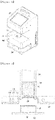
- the foreign substance detector is to detect foreign substances 11 attached onto the surface of a film 10 which is a foreign substance detection sample, and includes an optical unit 100, an optical housing 200 accommodating the optical unit 10 therein and formed in a through shape, a light emission unit 300 provided at a lower side of the optical housing 200 to emit light toward the film 10, wherein the light is to be emitted toward the film 10 from a direction of surrounding a circumference of the film 10, and a film holder 400 provided to be spaced apart from the lower side of the light emission unit 300 to provide a loading surface 410 so that the film 10 is to be loaded thereon and formed of a light-absorbing material capable of absorbing light or reflect the light at a predetermined ratio or less.
- the present invention further includes a holder supporter 500 supporting the film holder 400 from the lower portion of the film holder 400, and a light blocking plate 600 provided below the light emission unit 300 to block light emitted from an ambient external light source from being transmitted to the film 10 side.
- the film 10 is made of a transparent or translucent plastic material, and an adhesive layer for adsorbing the foreign substances is provided and a release paper is attached onto one surface of the film 10.
- the film 10 includes a configuration disclosed in Korean Patent Registration No. 10-1582461 (Title of the invention: Test film for detecting surface particles in clean room) previously registered by the applicant of the present invention.
- the optical unit 100 may be applied as a microscope, a magnifying glass, an image sensor, or the like, and in the exemplary embodiment of the present invention, as an example, the optical unit 100 may be applied as a microscope (including an electron microscope) that easily adjusts a focal length.
- the optical housing 200 is formed in a hollow through shape so as to accommodate the optical unit 100 therein.
- the optical housing 200 is provided with a control switch 210 so as to allow the inspector to easily control a focal length of the optical unit 100, that is, the microscope if necessary.
- a cutout may be formed so that a part of the control switch 210 is exposed to the outside of the optical housing 200 to be handled by the inspector by hand.
- the optical unit 100 can detect the number, size, distribution, and the like of the foreign substances by light which is emitted from a light source to be described below, reflected or scattered by the foreign substance on the film 10, and then introduced to the optical unit 100 again.
- the optical unit 100 observes a reflection light generation portion by the foreign substances, and since the reflection light does not occur in the portion without the foreign substances, the optical unit 100 detects the foreign substances through the result shown in the form of a dark or black region.
- the control switch 210 is provided in the optical housing 200, and the foreign substances are generated during the switch operation by the inspector to fall onto the upper portion of the film 10 along the inner space of the optical housing 200.
- foreign substances that are not actually foreign substances in the clean room, that is, are not detection targets are attached onto the film 10 to deteriorate the detection reliability of the foreign substances due to distortion of the detection result.
- the present invention provides a foreign substance fall prevention film 220 as illustrated in FIGS. 2 and 3 .
- the foreign substance fall prevention film 220 is provided below the optical housing 200, prevents foreign substance that may be generated in the optical housing 200 from falling onto the film 10, and may be made of a transparent material so as not to prevent the detection of the foreign substances of the optical unit 100.
- the foreign substance fall prevention film 220 may be made of any one material of glass, quartz, and acryl, and may be interchangeably installed in the optical housing 200 so as to facilitate surface cleaning after a long-term use. To this end, as illustrated in FIG.
- a prevention film cutout 230 may be provided in the optical housing 200, guide ribs 240 spaced apart from each other in a vertical direction may be provided to stably install the foreign substance fall prevention film 220 and guide the installation of the foreign substance fall prevention film 220 around the prevention film cutout 230, and the inspector may slidely move the foreign substance fall prevention film 220 in a lateral direction of the optical housing 200 so that the foreign substance fall prevention film 220 is able to be installed in or detached from the optical housing 200.
- a separate display 250 may be provided on the upper side of the optical housing 200 so that the inspector further enlarges an image detected from the optical unit 100, for example, a microscope so as to easily check the image.
- the light emission unit 300 emits light onto the film 10 and the optical unit 100 detects light reflected from the foreign substances to effectively detect the presence or absence of the foreign substances attached onto the surface of the film 10.
- the light emission unit 300 is spaced apart from the film 10 at a predetermined distance or more and configured to emit light toward the film 10 in a plurality of directions of the circumference of the film 10.
- An imaginary line of FIG. 2 means a housing forming an appearance.
- the light emission unit 300 may emit the light toward the film 10 in a plurality of directions, such as two directions, three directions, four directions, five directions, and six directions or more of the circumference of the film 10.
- the light emission unit 300 will be described based on a case of emitting light in four directions of the circumference of the film 10 for convenience of description, but is not necessarily limited to those described above.
- the light emission unit 300 includes a light emission body 310 in which an empty space is formed in a central region corresponding to an arrangement position of the film 10, first to fourth light sources 321, 322, 323, and 324 provided in the first to fourth sections 311, 312, 313, and 314 of the light emission body 310 corresponding to a circumferential direction including front and rear and left and right directions of the film 10 to emit the light to the film 10, and first to fourth light diffusion plates 331, 332, 333, and 334 diffusing the light emitted from the first to fourth light sources 321, 322, 323, and 324.
- the present invention is not limited thereto, and the sections may be formed in a ring shape surrounding the circumference of the film 10, and the light sources and the light diffusion plates may be disposed in the ring shape correspondingly.
- An opening 350 is formed in the central region of the light emission body 310 so that a lower end of the optical housing 200 is partially inserted, an empty space is provided to communicate with the opening 350, and the film 10 is positioned below the empty space.
- the first to fourth light sources 321, 322, 323, and 324 are applicable as an LED, a laser, and the like. When the light sources are applied as the LED, it is preferable that the light emitted at a predetermined light emission range angle or more is applied to have sufficient straightness.
- the first to fourth light diffusing plates 331, 332, 333, and 334 are provided between the film 10 and the first to fourth light sources 321, 322, 323, and 324, respectively, to increase the uniformity of the light quantity distribution on the surface of the film 10, thereby preventing the occurrence of a phenomenon that the foreign substance size is detected differently according to a difference in the light quantity distribution during the detection by a microscope, an image sensor, and the like.
- the light is emitted toward the foreign substances 11 attached onto the film 10 in four directions (front, rear, left, and right) of the film 10 to prevent the detection of the foreign substances from being omitted by the shaded section as described above, thereby improving measurement reliability.
- a reflective plate 370 may also be disposed to emit light in both directions facing each other based on the film 10 without disposing a separate light source in the rest of two directions.
- the light emitted from both light sources may be reflected to the reflective plates 370 on both sides to be emitted to the film 10 side again, thereby preventing the foreign substances from being not detected by the shaded section as described above.
- the reflective plate 370 may be applied with a material and a color capable of reflecting light in a predetermined amount or more, and for example, the reflective plate 370 may be applied in a white color.
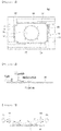
- the first to fourth light sources 321, 322, 323, and 324 are positioned above the film 10, and a light emission angle ⁇ of the first to fourth light sources 321, 322, 323, and 324 with respect to the film 10 is preferably in the range of 5° to 30°.
- the film 10 generally maintains a certain level or more of flatness, as illustrated in FIGS. 8(a) and 8(b) , there may be a shape deformation of the film such as bending the film convexly upwards or downwards by the heat generated from the light source.
- a shape deformation of the film such as bending the film convexly upwards or downwards by the heat generated from the light source.
- the present invention has advantages of preventing the detection of the foreign substances from being omitted even while the film 10 is not fully flat by applying emission angles of the first to fourth light sources 321, 322, 323, and 324 in the range of 5° to 30° and more compactly reducing the entire device by reducing an increase in the size of the light emission unit 300.
- the film holder 400 is spaced apart from the lower side of the light emission unit 300 to provide a loading surface 410 so that the film 10 is able to be loaded thereon and is made of a light-absorbing material capable of absorbing light or reflecting the light at a predetermined ratio or less.
- the film holder 400 may be formed in the shape of a hollow cube, a hollow cylinder, a hollow polyhedron, and the like, and a guide groove 420 is provided on the upper surface thereof to guide the loading position of the film 10, and a through hole 430 is provided in the guide groove 420.
- a microscope or a magnifying glass when the inspector inspects the transparent film 10 by using a microscope or a magnifying glass, if there is reflected light reflected from the film holder 400 under the transparent film 10, there may be a situation that it is difficult or impossible for the optical unit 100 to properly observe the foreign substances, and there may be a problem in that the foreign substances attached onto the inner surface of the film holder 400 are misrecognized as foreign substances of the film 10 which is a sample.
- the film holder 400 is made of a light-absorbing material of absorbing light or reflecting the light at a predetermined ratio or less.
- the film holder 400 may be made of an aluminum material and sandblasts and then black-anodizes the surface thereof (including an inner surface) after sandblasting so as to prevent the light reflection.
- the film holder 400 may have a predetermined inner area depth H or more so that the light emitted from the light emission unit 300 passes through the film 10, passes through the through hole 430 to be reflected or scattered on its inner bottom surface, and then is not introduced within a focal length of the optical unit 100 again. That is, in the present invention, the film holder 400 has a sufficient inner depth to prevent the occurrence of an error in which the foreign substances present in the film holder 400 are attached onto the lower surface of the film 10 to be detected together with the foreign substances which are normal detected targets attached onto the upper surface of the film 10.
- the holder supporter 500 is to support the film holder 400 from the lower side, and in the exemplary embodiment of the present invention, the holder supporter may be made of a material capable of generating a predetermined electric force or more between the holder supporter and the foreign substances floating in the atmosphere of the surrounding space.
- the holder supporter 500 is applied as a material that generates a predetermined electric force or more between the holder supporter and the foreign substances floating in the atmosphere of the surrounding space to prevent the foreign substances generated in the inspector and during the inspection from being moved to the surface of the film 10, and specifically, the foreign substances are moved to the holder supporter 500 side before being moved to the surface of the film 10, thereby improving the measurement reliability.
- the holder supporter 500 allows the foreign substances generated in the inspector and during the inspection to be attached onto the surface of the supporter 500 before being moved to the film 10, thereby minimizing the movement to the film 10 of the surrounding foreign substances.
- a material of the holder supporter 500 is applicable as Teflon, PVC, polystyrene, polyester, and the like.
- the light blocking plate 600 blocks external light so that the light emitted from external light sources around the inspection space other than the first to fourth light sources 321, 322, 323, and 324 of the light emission unit 300 is transmitted to the film 10 side to be prevented from affecting detection accuracy of the foreign substances. That is, a central space (film surrounding space) of the light emission unit 300 may be created in a kind of dark atmosphere by the light blocking plate 600.
- the light blocking plate 600 is provided to extend to the outside of the light emission unit 300 by a predetermined length or more and made of a light-absorbing material capable of absorbing light or reflecting the light at a predetermined ratio or less.
- the light blocking plate 600 may be made of the same/similar aluminum material as/to the film holder 400, and sandblasts and then black-anodizes the surface thereof to prevent light reflection.
- the film 10 should maintain the flatness as a whole to increase the detection accuracy of the foreign substances.
- heat generated from the first to fourth light sources 321, 322, 323, and 324 of the light emission unit 300 is transmitted to the film 10, and the film 10 is prevented from being bent or damaged by the heat.
- the focal point of the optical unit 100 is changed to cause an error in detection.
- the optical housing 200 and the light blocking plate 600 are made of a thermally conductive material having a predetermined thermal conductivity or higher, respectively, thereby dissipating the heat generated from the light emission unit 300 to the outside.
- the holder supporter is manufactured using a material capable of generating a predetermined electrostatic force or more between the holder supporter and the foreign substances floating in a surrounding space to prevent foreign substances floating or scattered in the surrounding workspace from being moved to the film side, thereby improving detection reliability.
Landscapes
- Physics & Mathematics (AREA)
- Chemical & Material Sciences (AREA)
- General Physics & Mathematics (AREA)
- Life Sciences & Earth Sciences (AREA)
- Pathology (AREA)
- Analytical Chemistry (AREA)
- Biochemistry (AREA)
- General Health & Medical Sciences (AREA)
- Health & Medical Sciences (AREA)
- Immunology (AREA)
- Nonlinear Science (AREA)
- Engineering & Computer Science (AREA)
- Computer Vision & Pattern Recognition (AREA)
- Signal Processing (AREA)
- Crystallography & Structural Chemistry (AREA)
- Optics & Photonics (AREA)
- Dispersion Chemistry (AREA)
- Investigating Materials By The Use Of Optical Means Adapted For Particular Applications (AREA)
Applications Claiming Priority (2)
| Application Number | Priority Date | Filing Date | Title |
|---|---|---|---|
| KR1020170098091A KR101809009B1 (ko) | 2017-08-02 | 2017-08-02 | 투명 또는 반투명 필름의 표면 이물 검출기 |
| PCT/KR2018/007333 WO2019027143A1 (fr) | 2017-08-02 | 2018-06-28 | Détecteur de substances étrangères de surface pour film transparent ou translucide |
Publications (3)
| Publication Number | Publication Date |
|---|---|
| EP3663746A1 true EP3663746A1 (fr) | 2020-06-10 |
| EP3663746A4 EP3663746A4 (fr) | 2021-04-28 |
| EP3663746B1 EP3663746B1 (fr) | 2026-08-05 |
Family
ID=60954426
Family Applications (1)
| Application Number | Title | Priority Date | Filing Date |
|---|---|---|---|
| EP18840625.0A Active EP3663746B1 (fr) | 2017-08-02 | 2018-06-28 | Détecteur de substances étrangères de surface pour film transparent ou translucide |
Country Status (5)
| Country | Link |
|---|---|
| US (1) | US11002685B2 (fr) |
| EP (1) | EP3663746B1 (fr) |
| KR (1) | KR101809009B1 (fr) |
| CN (1) | CN111133299B (fr) |
| WO (1) | WO2019027143A1 (fr) |
Families Citing this family (4)
| Publication number | Priority date | Publication date | Assignee | Title |
|---|---|---|---|---|
| KR101970220B1 (ko) | 2018-11-20 | 2019-04-18 | 주식회사 제덱스 | 여과재를 이용한 유체 중의 실시간 이물 계수 장치 |
| KR102644345B1 (ko) * | 2021-04-20 | 2024-03-06 | 제이 머티리얼즈(주) | 캐리어 표면의 이물질 검사장치 |
| KR102485850B1 (ko) * | 2022-08-18 | 2023-01-09 | 주식회사 제덱스 | 광산란과 이미지 분석을 이용한 광학 이물질 검출 장치 |
| US12099184B1 (en) * | 2023-10-20 | 2024-09-24 | Pramana Inc. | System and methods for detecting and cleaning contaminants from an imaging optical path |
Family Cites Families (19)
| Publication number | Priority date | Publication date | Assignee | Title |
|---|---|---|---|---|
| US4152053A (en) * | 1976-06-28 | 1979-05-01 | Menary Robert F | Film inspection machine |
| JP2820573B2 (ja) * | 1992-08-28 | 1998-11-05 | 三菱電機株式会社 | 距離測定装置 |
| JP3009659B1 (ja) * | 1998-12-09 | 2000-02-14 | 株式会社日本マクシス | 傷検査用光源及び傷検査用光源ユニット |
| JP2000180371A (ja) | 1998-12-11 | 2000-06-30 | Sharp Corp | 異物検査装置および半導体工程装置 |
| SE521948C2 (sv) * | 1998-12-17 | 2003-12-23 | Act Ab | Mätinstrument och förfarande för mätning av damm- och smutsbeläggningsgrad på en yta |
| US6449035B1 (en) * | 1999-05-12 | 2002-09-10 | John Samuel Batchelder | Method and apparatus for surface particle detection |
| US6864973B2 (en) * | 1999-12-30 | 2005-03-08 | Eastman Kodak Company | Method and apparatus to pre-scan and pre-treat film for improved digital film processing handling |
| JP4713185B2 (ja) * | 2005-03-11 | 2011-06-29 | 株式会社日立ハイテクノロジーズ | 異物欠陥検査方法及びその装置 |
| JP2007057315A (ja) * | 2005-08-23 | 2007-03-08 | Pioneer Electronic Corp | 表面検査装置 |
| KR101042143B1 (ko) | 2007-01-15 | 2011-06-16 | 에스엔유 프리시젼 주식회사 | 평판표시장치의 이물 검사기 |
| JP5171524B2 (ja) * | 2007-10-04 | 2013-03-27 | 株式会社日立ハイテクノロジーズ | 物体表面の欠陥検査装置および方法 |
| JP4388986B2 (ja) * | 2008-03-19 | 2009-12-24 | シャープ株式会社 | シート積層体の清掃装置およびシート積層体の清掃方法 |
| KR101240564B1 (ko) | 2009-09-02 | 2013-03-14 | 아주하이텍(주) | 광학 검사 장치 및 이를 이용한 검사 방법 |
| JP5656055B2 (ja) * | 2009-09-29 | 2015-01-21 | Nltテクノロジー株式会社 | 光学素子の製造方法、光学素子用露光装置、光学素子、照明光学装置、表示装置、および電子機器 |
| NL2010544A (en) * | 2012-04-02 | 2013-10-03 | Asml Netherlands Bv | Particulate contamination measurement method and apparatus. |
| JP2015145807A (ja) * | 2014-02-03 | 2015-08-13 | 学校法人同志社 | 微粒子検出装置 |
| JP6438703B2 (ja) * | 2014-08-21 | 2018-12-19 | バンドー化学株式会社 | 異物検査装置、異物検査システム及び異物検査方法 |
| KR101582461B1 (ko) * | 2014-10-22 | 2016-01-05 | 주식회사 제덱스 | 클린룸의 표면 입자 검출용 시험 필름 |
| CN104438226B (zh) * | 2014-12-02 | 2016-07-27 | 京东方科技集团股份有限公司 | 掩膜板清洁系统 |
-
2017
- 2017-08-02 KR KR1020170098091A patent/KR101809009B1/ko active Active
-
2018
- 2018-06-28 EP EP18840625.0A patent/EP3663746B1/fr active Active
- 2018-06-28 CN CN201880057116.5A patent/CN111133299B/zh active Active
- 2018-06-28 WO PCT/KR2018/007333 patent/WO2019027143A1/fr not_active Ceased
- 2018-06-28 US US16/643,392 patent/US11002685B2/en active Active
Also Published As
| Publication number | Publication date |
|---|---|
| US11002685B2 (en) | 2021-05-11 |
| WO2019027143A1 (fr) | 2019-02-07 |
| US20200292461A1 (en) | 2020-09-17 |
| KR101809009B1 (ko) | 2017-12-15 |
| CN111133299A (zh) | 2020-05-08 |
| EP3663746B1 (fr) | 2026-08-05 |
| CN111133299B (zh) | 2022-07-29 |
| EP3663746A4 (fr) | 2021-04-28 |
Similar Documents
| Publication | Publication Date | Title |
|---|---|---|
| US11002685B2 (en) | Surface foreign substance detector for transparent or translucent film | |
| US6901314B2 (en) | Alignment apparatus for substrates | |
| US7420671B2 (en) | Defect inspection method and apparatus for transparent plate-like members | |
| JP2020025126A (ja) | イメージングシステム | |
| US9588056B2 (en) | Method for particle detection on flexible substrates | |
| WO2012173692A1 (fr) | Alignement de masque de dépôt chimique en phase vapeur pour traitement d'une delo | |
| JPWO2019212011A1 (ja) | 検査装置 | |
| JP5648874B2 (ja) | マクロ検査装置 | |
| NL2033683B1 (en) | Method for inspecting a photomask contained in a transparent pod | |
| JP6570084B2 (ja) | ステージ表面上の突起物の上面を検査するマクロ検査装置 | |
| JP2007248292A (ja) | 外観検査装置 | |
| JP2009174957A (ja) | 異物検出方法および装置 | |
| CN206891991U (zh) | 检测系统 | |
| EP3413037A1 (fr) | Dispositif d'inspection pour objets en feuilles, et procédé d'inspection pour objets en feuilles | |
| JP6769796B2 (ja) | ロボットのハンド部の傾き検査装置及びその傾き検査方法 | |
| JP2009236732A (ja) | 基板検査装置 | |
| JP4563847B2 (ja) | 基板検査装置 | |
| KR0147600B1 (ko) | 음극선관 패널의 결함 검사장치 | |
| JP4408369B2 (ja) | 目視検査台 | |
| TW201133691A (en) | A test system for detecting shape and/or orientation errors of wafers | |
| JPH08304048A (ja) | 凹凸欠陥検査装置 | |
| CN109426012B (zh) | 一种用于显示屏检测的背光治具 | |
| CN215640821U (zh) | 镜筒组件、检测装置及检测设备 | |
| KR101185076B1 (ko) | 반사체용 반사형 광센서 | |
| KR20140001508U (ko) | 기판 검사장치 |
Legal Events
| Date | Code | Title | Description |
|---|---|---|---|
| STAA | Information on the status of an ep patent application or granted ep patent |
Free format text: STATUS: THE INTERNATIONAL PUBLICATION HAS BEEN MADE |
|
| PUAI | Public reference made under article 153(3) epc to a published international application that has entered the european phase |
Free format text: ORIGINAL CODE: 0009012 |
|
| STAA | Information on the status of an ep patent application or granted ep patent |
Free format text: STATUS: REQUEST FOR EXAMINATION WAS MADE |
|
| 17P | Request for examination filed |
Effective date: 20200224 |
|
| AK | Designated contracting states |
Kind code of ref document: A1 Designated state(s): AL AT BE BG CH CY CZ DE DK EE ES FI FR GB GR HR HU IE IS IT LI LT LU LV MC MK MT NL NO PL PT RO RS SE SI SK SM TR |
|
| AX | Request for extension of the european patent |
Extension state: BA ME |
|
| DAV | Request for validation of the european patent (deleted) | ||
| DAX | Request for extension of the european patent (deleted) | ||
| REG | Reference to a national code |
Ref country code: DE Ref legal event code: R079 Free format text: PREVIOUS MAIN CLASS: G01N0021880000 Ipc: G01N0021940000 |
|
| A4 | Supplementary search report drawn up and despatched |
Effective date: 20210331 |
|
| RIC1 | Information provided on ipc code assigned before grant |
Ipc: G01N 21/94 20060101AFI20210325BHEP Ipc: G01N 21/958 20060101ALI20210325BHEP Ipc: G01N 1/28 20060101ALI20210325BHEP |
|
| STAA | Information on the status of an ep patent application or granted ep patent |
Free format text: STATUS: EXAMINATION IS IN PROGRESS |
|
| 17Q | First examination report despatched |
Effective date: 20221207 |
|
| GRAP | Despatch of communication of intention to grant a patent |
Free format text: ORIGINAL CODE: EPIDOSNIGR1 |
|
| STAA | Information on the status of an ep patent application or granted ep patent |
Free format text: STATUS: GRANT OF PATENT IS INTENDED |
|
| RIC1 | Information provided on ipc code assigned before grant |
Ipc: G01N 21/94 20060101AFI20260323BHEP Ipc: G01N 21/958 20060101ALI20260323BHEP Ipc: G01N 1/28 20060101ALI20260323BHEP Ipc: G01N 15/06 20060101ALI20260323BHEP |
|
| INTG | Intention to grant announced |
Effective date: 20260416 |
|
| GRAS | Grant fee paid |
Free format text: ORIGINAL CODE: EPIDOSNIGR3 |
|
| GRAA | (expected) grant |
Free format text: ORIGINAL CODE: 0009210 |
|
| STAA | Information on the status of an ep patent application or granted ep patent |
Free format text: STATUS: THE PATENT HAS BEEN GRANTED |
|
| AK | Designated contracting states |
Kind code of ref document: B1 Designated state(s): AL AT BE BG CH CY CZ DE DK EE ES FI FR GB GR HR HU IE IS IT LI LT LU LV MC MK MT NL NO PL PT RO RS SE SI SK SM TR |
|
| REG | Reference to a national code |
Ref country code: CH Ref legal event code: F10 Free format text: ST27 STATUS EVENT CODE: U-0-0-F10-F00 (AS PROVIDED BY THE NATIONAL OFFICE) Effective date: 20260805 Ref country code: GB Ref legal event code: FG4D |