EP3663752B1 - Thermischer flusssensor mit heizbaren nanodrähten - Google Patents
Thermischer flusssensor mit heizbaren nanodrähten Download PDFInfo
- Publication number
- EP3663752B1 EP3663752B1 EP19213402.1A EP19213402A EP3663752B1 EP 3663752 B1 EP3663752 B1 EP 3663752B1 EP 19213402 A EP19213402 A EP 19213402A EP 3663752 B1 EP3663752 B1 EP 3663752B1
- Authority
- EP
- European Patent Office
- Prior art keywords
- sensor
- nanofilaments
- nanofilament
- support
- resonator
- Prior art date
- Legal status (The legal status is an assumption and is not a legal conclusion. Google has not performed a legal analysis and makes no representation as to the accuracy of the status listed.)
- Active
Links
Images


Classifications
-
- G—PHYSICS
- G01—MEASURING; TESTING
- G01N—INVESTIGATING OR ANALYSING MATERIALS BY DETERMINING THEIR CHEMICAL OR PHYSICAL PROPERTIES
- G01N29/00—Investigating or analysing materials by the use of ultrasonic, sonic or infrasonic waves; Visualisation of the interior of objects by transmitting ultrasonic or sonic waves through the object
- G01N29/02—Analysing fluids
- G01N29/022—Fluid sensors based on microsensors, e.g. quartz crystal-microbalance [QCM], surface acoustic wave [SAW] devices, tuning forks, cantilevers, flexural plate wave [FPW] devices
-
- G—PHYSICS
- G01—MEASURING; TESTING
- G01K—MEASURING TEMPERATURE; MEASURING QUANTITY OF HEAT; THERMALLY-SENSITIVE ELEMENTS NOT OTHERWISE PROVIDED FOR
- G01K17/00—Measuring quantity of heat
- G01K17/06—Measuring quantity of heat conveyed by flowing media, e.g. in heating systems e.g. the quantity of heat in a transporting medium, delivered to or consumed in an expenditure device
-
- B—PERFORMING OPERATIONS; TRANSPORTING
- B81—MICROSTRUCTURAL TECHNOLOGY
- B81B—MICROSTRUCTURAL DEVICES OR SYSTEMS, e.g. MICROMECHANICAL DEVICES
- B81B7/00—Microstructural systems; Auxiliary parts of microstructural devices or systems
- B81B7/008—MEMS characterised by an electronic circuit specially adapted for controlling or driving the same
-
- G—PHYSICS
- G01—MEASURING; TESTING
- G01N—INVESTIGATING OR ANALYSING MATERIALS BY DETERMINING THEIR CHEMICAL OR PHYSICAL PROPERTIES
- G01N29/00—Investigating or analysing materials by the use of ultrasonic, sonic or infrasonic waves; Visualisation of the interior of objects by transmitting ultrasonic or sonic waves through the object
- G01N29/02—Analysing fluids
- G01N29/036—Analysing fluids by measuring frequency or resonance of acoustic waves
-
- B—PERFORMING OPERATIONS; TRANSPORTING
- B81—MICROSTRUCTURAL TECHNOLOGY
- B81B—MICROSTRUCTURAL DEVICES OR SYSTEMS, e.g. MICROMECHANICAL DEVICES
- B81B2201/00—Specific applications of microelectromechanical systems
- B81B2201/02—Sensors
- B81B2201/0271—Resonators; ultrasonic resonators
-
- G—PHYSICS
- G01—MEASURING; TESTING
- G01N—INVESTIGATING OR ANALYSING MATERIALS BY DETERMINING THEIR CHEMICAL OR PHYSICAL PROPERTIES
- G01N2291/00—Indexing codes associated with group G01N29/00
- G01N2291/02—Indexing codes associated with the analysed material
- G01N2291/028—Material parameters
- G01N2291/02881—Temperature
-
- G—PHYSICS
- G01—MEASURING; TESTING
- G01N—INVESTIGATING OR ANALYSING MATERIALS BY DETERMINING THEIR CHEMICAL OR PHYSICAL PROPERTIES
- G01N2291/00—Indexing codes associated with group G01N29/00
- G01N2291/04—Wave modes and trajectories
- G01N2291/042—Wave modes
- G01N2291/0427—Flexural waves, plate waves, e.g. Lamb waves, tuning fork, cantilever
Definitions
- the present invention relates to a thermal flux sensor with heating nanofilaments.
- a heat flux sensor can find an application in particular in a gas sensor, a gas analysis system or a flowmeter.
- a heat flux sensor makes it possible to measure a heat exchange between the body of the sensor and its surrounding environment.
- the surrounding medium can be a gaseous or liquid medium. This approach can be used to produce, for example, a gas sensor or a pressure sensor.
- a gas sensor of the TCD type (acronym of the Anglo-Saxon term “Thermal Conductivity Detector” or “thermal conductivity detector”) operates on the principle of measuring the electrical resistance of a wire whose temperature varies according to the exchanges heat with a surrounding gas through the thermal conductivity of said gas.
- Such a sensor is described in particular in the document US 8,313,236 .
- Such a sensor can be arranged at the outlet of a gas chromatography column through which the different species constituting a mixture of gases to be analyzed are separated.
- the sensor comprises a heating wire coupled to an electric source making it possible to heat it by Joule effect, suspended in a volume in which there are one or more species to be detected.
- the heat exchanges between the heating wire and the species are likely to cause a variation in temperature of the heating wire and consequently a variation in the electrical resistance of the wire.
- the wire is generally made of platinum coated with nitride, which are materials with high levels of stress, causing difficulties implementation and limitations in terms of sensor design. This technology is therefore difficult to master in practice.
- Another type of sensor based on the same measurement principle has been produced on a silicon substrate using microfabrication techniques, allowing the heating wire to be etched directly in a layer of silicon.
- This type of sensor has been described in the documents FR 2 995 691 , FR 2 995 690 And FR 2 995 692 . This technique has an advantage in terms of ease of integration.
- the document WO 2015/082956 describes a resonator of the NEMS type (acronym of the Anglo-Saxon term “Nano Electro-Mechanical Systems”) allowing the measurement of the gas concentration by gravimetric effect, that is to say the modification of the resonant frequency of the resonator due to a modification of the mass of the resonant structure.
- An object of the invention is to design a heat flux sensor which is simple to manufacture, while ensuring good detection sensitivity.
- nanometric size a filament of nanometric size, that is to say of which one of the transverse dimensions (for example the diameter in the case of a round filament, or the width in the case of of a filament with a rectangular section) is less than or equal to a few hundred nm, for example less than 500 nm.
- Such a sensor is based on the fact that the resonant frequency of the resonator strongly depends on the intensity of the electric current passing through it.
- This sensor benefits from the measurement precision offered by NEMS resonators, while ensuring a sufficiently large heat exchange with the gas to be detected thanks to the network of heating nanofilaments, this heat exchange inducing a variation in the electrical resistance of the nanofilaments and therefore the intensity of the electric current flowing through them.
- the invention also relates to a gas sensor comprising a heat flux sensor as described above.
- the invention also relates to a gas analysis system comprising a chromatography column and at least one sensor as described above arranged at the outlet of said chromatography column.
- the invention also relates to a flow meter comprising a heat flux sensor as described above.
- the heat flux sensor comprises a network of heating nanofilaments which are intended to be brought into contact with a fluid and to exchange heat with said fluid to enable a characteristic thereof to be measured.
- the heating nanofilaments comprise an electrically conductive material having a determined electrical resistivity or a semiconductor material; they are connected, via a support, to an electrical source adapted to bring said nanofilaments to a temperature determined by the Joule effect.
- the array of heating nanofilaments is designed to allow maximum heat exchange with the surrounding fluid and minimize heat loss with the medium.
- the heating nanofilaments are therefore advantageously suspended relative to the support, that is to say that a free space is left between each heating nanofilament and the support to allow the fluid to surround each heating nanofilament on all its faces and to maximize the contact surface between the fluid and the heating nanofilament.
- a modification of the composition of the gas surrounding the sensor modifies the heat exchanges between the nanofilaments and the gas, and therefore causes the temperature of the heating nanofilaments to vary; the measurement of this temperature makes it possible to deduce the composition of the gas.
- a speed variation of a flow of gas surrounding the sensor modifies the heat exchanges between the nanofilaments and the gas and therefore also causes the temperature of the nanofilaments to vary.
- the thermal flow sensor combines said network of heating nanofilaments with at least one resonator of the nano electromechanical system (NEMS) type arranged on one side of said network and secured to the support, said resonator playing the role of a temperature sensor.
- NEMS nano electromechanical system
- such a NEMS resonator comprises a beam suspended relative to the support, an actuation device capable of generating a vibration of said beam under the effect of an excitation signal, and a detection configured to measure a displacement of said beam during said vibration and emit an output signal having a resonance at the resonant frequency of the resonator, said resonant frequency depending on the temperature of the beam.
- the beam is one of the heating nanofilaments of the network, more precisely a nanofilament located on one side of the network.
- the sensor comprises two NEMS resonators, the respective beam of which is a nanofilament arranged on one side of the network.
- the implementation of two resonators arranged symmetrically with respect to the network has the advantage of allowing a differential measurement which simplifies the detection signal processing and improves the signal to noise ratio during detection.
- the material of the heating nanofilaments is characterized by a thermal coefficient of resistance (TCR, acronym of the Anglo-Saxon term “temperature coefficient of resistance”) which defines the variation of its electrical resistivity as a function of temperature. Consequently, a variation in the temperature of the network of heating nanofilaments by heat exchange with the surrounding fluid causes a variation in the electrical resistance of the nanofilaments and therefore the variation in the intensity of the electric current which passes through them.
- TCR thermal coefficient of resistance
- the beam being polarized at the same potential as the other nanofilaments, it also undergoes a variation of the electric current which crosses it, which strongly affects the resonant frequency of the resonator.
- the actuation device is of the electrostatic type.
- the actuation device comprises an electrode located on one side of the beam, at a distance therefrom. This distance is of the order of a few hundred nm.
- the detection device is of the piezoresistive type, as described in the document FR 2 996 219 .
- a piezoresistive strain gauge is located on one side of the beam, at a distance from its two ends.
- the dimensions of this gauge are typically from a few tens to a few hundreds of nm in width and thickness and a few hundreds of nm to a few ⁇ m in length.
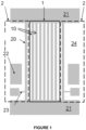
- FIG. 1 illustrates an embodiment of the thermal flux sensor, comprising two NEMS resonators arranged on either side of the network of heating nanofilaments.
- the network 1 comprises nanofilaments 10 and two beams 20 which are two nanofilaments forming the two sides of the network. Each nanofilament is embedded at each of its two ends in a support 21.
- each resonator 2 comprises an actuation device, represented in the form of an electrode 22 in the illustrated embodiment, as well as a detection device comprising a piezoresistive gauge 23.
- the two resonators are symmetrical by relative to a longitudinal axis of the network 1.
- the network of nanofilaments is configured to exhibit high sensitivity.
- the number and size of the nanofilaments are chosen so that the network has a large heat exchange surface with the surrounding fluid.
- the number of heating nanofilaments is typically between 10 and 1000.
- each heating nanofilament is arranged at a distance from an adjacent heating nanofilament.
- the distance between two adjacent nanofilaments is between 0.5 and 1.5 ⁇ m, for example of the order of 1 ⁇ m.
- the junction between the heating nanofilaments and their support is sized to minimize heat losses at this junction.
- the typical dimensions of the nanofilaments are as follows: a section whose width and height are from a few tens to hundreds of nm per side, and a length from a few ⁇ m to a few tens of ⁇ m.
- the heating nanofilaments can consist of a semiconductor material, such as silicon (monocrystalline or polycrystalline, doped or not), germanium, silicon-germanium (SiGe).
- the silicon may be porous, the porosity making it possible to increase the heat exchanges with the surrounding environment.
- the beams are made of the same material as the heating nanofilaments, possibly with different doping levels chosen so that the electrical resistance of the heating nanofilaments is greater than that of the beam.
- the beam of each NEMS resonator is constituted by a heating nanofilament does not imply that said beam necessarily has the same dimensions as the other heating nanofilaments.
- the section of the beams is of the same order of magnitude as that of the nanofilaments because the beams and the nanofilaments are preferably made with the same technology.
- the length of the beams it can be the same as that of the nanofilaments or different.
- the choice of the resonant frequency of the resonator may require the choice of a length of the beam different from the length of the other heating nanofilaments.
- the resonant frequency of each resonator is a few MHz to a few hundred MHz.
- the heating nanofilaments are shown rectilinear and parallel to each other in the appended figures, other embodiments are possible.
- the nanofilaments may not be parallel to each other; moreover, the nanofilaments can have a non-rectilinear shape, for example a serpentine shape, which makes it possible to increase the length of the heating nanofilaments while releasing any compressive stresses.
- FIG. 1 is an electrical diagram of the heat flux sensor.
- each heating nanofilament is represented in the form of an electrical resistance denoted R TCD i for the i th nanofilament, i being an integer varying between 1 and n (n being the total number of heating nanofilaments excluding the nanofilaments constituting the beams of the resonators). All the electrical resistors have substantially the same value since the nanofilaments have identical dimensions and are made of the same material.
- each beam is represented in the form of an electrical resistor denoted R NEMS 1 or R NEMS 2 .
- All of the heating beams and nanofilaments are arranged in parallel and connected by one end to a first potential (for example to ground) and by the opposite end to a second potential, denoted V TCD bias .
- Each beam is actuated in vibration at its resonant frequency by an electrode brought to an actuation potential V NEMS .
- Each piezoresistive gauge is represented in the form of an electrical resistance denoted R J1 or R J2 .
- Each gauge is current-biased, the intensity of which is denoted I bias1 or I bias2 respectively.
- I bias1 (or I bias2 ) is very small compared to the product of R NEMS 1 (or R NEMS 2 ) and V TCD bias , which is equal to the product of R TCD i and V TCD bias , then we consider that R NEMS 1 (or R NEMS 2 ) is equal to R TCD i .
- This variation in the intensity of the electric current generates a variation in the resonance frequency which is measured by the piezoresistive gauges.
- a preferred manufacturing method is based on a semiconductor on insulator (SOI, acronym for the English term “Semiconductor on insulator”) substrate.
- SOI semiconductor on insulator
- Such an SOI substrate successively comprises, from its surface, a thin layer of monocrystalline silicon (a few hundred nanometers thick), a buried dielectric layer (for example a layer of silicon oxide (SiO 2 ) and a base substrate, for example made of silicon, which serves as a mechanical support for the sensor.
- This method uses conventional microelectronics techniques, in particular photolithography, implantation, deposition and etching techniques.
- Species chosen to obtain the desired electrical resistivity are implanted in the thin layer of silicon in the zones intended to respectively form the heating nanofilaments and the resonator(s) (beam, strain gauges, actuating electrodes). These electrical resistivities may possibly be different between these two zones.
- the mechanical structures (heating nanofilaments, resonator(s) (beam, strain gauges, actuation electrodes), embeddings, etc.) are then etched anisotropically in the thin superficial silicon layer.
- the heating nanofilaments and the resonator are therefore formed in one piece with the support in said thin layer, and thus have the same thickness.
- the recesses are advantageously made large enough to ensure good mechanical strength with respect to the support after the release of the mechanical structures.
- the embedments thus typically have sides of several ⁇ m to tens of ⁇ m.
- the metallic interconnections are produced between the mechanical structures in doped silicon.
- an isotropic etching of the buried silicon oxide layer of the SOI substrate is carried out to release the mechanical silicon structures intended to be suspended (heating nanofilaments, resonator(s)) relative to the base substrate.
- the oxide layer is not etched - or is only partially etched - at the recesses.
- Said channel can be fluidically connected to the outlet of a gas chromatography column if such a column is implemented upstream of the sensor to separate and identify the compounds of the gas mixture.
- the senor can be used in a flow meter to measure gas flow.
- FIG. 3 is a block diagram of a heat flux sensor according to a variant of the sensor of the figure 1 .
- the beams 20 have a different length (lower in the figure) than that of the nanofilaments 10.
- one of the supports 21 in which the nanofilaments are embedded has an extension 210.
- One end of the beams is embedded in said extension 210 while the other end is embedded in the support 21 opposite.
- FIG 4 is a block diagram of a heat flux sensor according to a variant of the sensor of the picture 3 .
- the nanofilaments 10 are mechanically connected by bridges 11 which increase the mechanical rigidity of the network 1.
- Said bridges are advantageously made in one piece with the nanofilaments during manufacture of the network.
- the bridges extend advantageously perpendicular to the nanofilaments, although other arrangements of the bridges are possible.
- the bridges can extend parallel to each other with a distance of the order of 10 ⁇ m between two adjacent bridges.
- the beams are not connected to the other nanofilaments by such bridges, so as not to stiffen the beams and thus modify their resonance frequency and reduce the sensitivity of the resonators.
- FIG. 5 is a block diagram of a heat flux sensor according to a variant of the sensor of the picture 3 .
- the semiconductor material of the support 21, that of the resonators 2 (beams 20 and nanogauges 23) and that of the network of nanofilaments are implanted in a differentiated manner in order to adjust the electrical resistances in a differentiated manner.
- the implantation zones are schematized by the rectangles l1, l2.
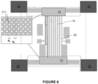
- FIG. 6 is a block diagram of a particular embodiment of the heat flux sensor.
- the structure consisting of the network of nanofilaments 10, of the resonator 2 and of the support 21 is suspended with respect to a substrate 24, which makes it possible to limit the thermal losses at the level of the recesses.
- the support 21 has a plurality of through holes 211 extending transversely to a main surface of the substrate 24. These holes 211 are distributed over at least part of the surface of the support 21. These holes can be used during process for manufacturing the sensor, to facilitate the etching of a sacrificial layer arranged under the support and the heating nanofilaments with a view to releasing the network of nanofilaments and the support and suspending them with respect to the substrate.
- each hole 211 has a diameter d 1 of the order of 0.5 ⁇ m and is separated from an adjacent hole by a distance d 2 of the order of 2 ⁇ m.
- d 1 of the order of 0.5 ⁇ m
- d 2 of the order of 2 ⁇ m.
Landscapes
- Physics & Mathematics (AREA)
- General Physics & Mathematics (AREA)
- Chemical & Material Sciences (AREA)
- Engineering & Computer Science (AREA)
- Health & Medical Sciences (AREA)
- Pathology (AREA)
- Immunology (AREA)
- Acoustics & Sound (AREA)
- General Health & Medical Sciences (AREA)
- Life Sciences & Earth Sciences (AREA)
- Analytical Chemistry (AREA)
- Biochemistry (AREA)
- Combustion & Propulsion (AREA)
- Microelectronics & Electronic Packaging (AREA)
- Computer Hardware Design (AREA)
- Micromachines (AREA)
- Investigating Or Analyzing Materials Using Thermal Means (AREA)
- Measuring Temperature Or Quantity Of Heat (AREA)
Claims (22)
- Thermischer Flusssensor, umfassend:- ein Netz (1) aus Nanofilamenten (10, 20), die im Verhältnis zu einer Halterung (21) aufgehängt sind, wobei jedes Nanofilament ein elektrisch leitendes oder halbleitendes Material umfasst, wobei das Netz durch eine Stromquelle polarisierbar ist, damit ein elektrischer Strom in jedem der Nanofilamente fließt,- mindestens einen Resonator (2) vom Typ elektromechanisches Nanosystem (NEMS), der umfasst:* einen Träger (20), der aus einem Nanofilament besteht, das eine Seite des Netzes bildet,* eine Betätigungseinrichtung (22), die in der Lage ist, durch ein Anregungssignal eine Vibration des betreffenden Trägers (20) zu erzeugen,* eine Erkennungsvorrichtung, die ausgelegt ist, um während der Vibration eine Verlagerung des Trägers (20) zu messen und ein Ausgangssignal zu senden, das eine Resonanz in der Resonanzfrequenz des Resonators aufweist, wobei die Resonanzfrequenz von der Stärke des elektrischen Stroms abhängt, der den Träger (20) durchquert, wobei eine Temperaturänderung des Netzes heizender Nanofilamente, die durch eine Änderung einer Eigenschaft eines Fluids in der Umgebung des Netzes hervorgerufen wird, eine Änderung der Stromstärke bewirkt, die den Träger durchquert, die zu einer Änderung der Resonanzfrequenz des Resonators führt.
- Sensor nach Anspruch 1, umfassend mindestens zwei Resonatoren (2), deren Träger (20) entlang zwei gegenüberliegender Seiten des Nanofilamentnetzes (1) eingerichtet sind.
- Sensor nach einem der Ansprüche 1 oder 2, wobei jedes Nanofilament (10, 20) an seinen beiden Enden in die Halterung (21) eingebettet ist.
- Sensor nach einem der Ansprüche 1 bis 3, wobei alle Nanofilamente (10, 20) des Netzes denselben Querschnitt haben.
- Sensor nach einem der Ansprüche 1 bis 4, wobei der Querschnitt jedes Nanofilaments (10, 20) eine Breite und Dicke von jeweils 10 bis 500 nm aufweist.
- Sensor nach einem der Ansprüche 1 bis 5, wobei jedes Nanofilament (10, 20) beabstandet von einem benachbarten Nanofilament eingerichtet ist.
- Sensor nach Anspruch 6, wobei der Abstand zwischen zwei benachbarten Nanofilamenten (10, 20) zwischen 0,5 und 1,5 µm liegt.
- Sensor nach einem der Ansprüche 1 bis 7, wobei die Träger (20) eine Länge haben, die sich von der der anderen Nanofilamente (10) unterscheidet.
- Sensor nach einem der Ansprüche 1 bis 8, wobei jedes Nanofilament (10) aus einem Halbleitermaterial wie Silizium besteht.
- Sensor nach Anspruch 9, wobei jeder Resonator ein Dotierungsniveau aufweist, das sich von dem der anderen Nanofilamente (10) unterscheidet.
- Sensor nach einem der Ansprüche 9 oder 10, wobei die Halterung (21) aus demselben Halbleitermaterial wie die Nanofilamente (10) besteht und die Halterung (21) ein anderes Dotierungsniveau als die Nanofilamente (10) aufweist, die keine Träger (20) sind.
- Sensor nach einem der Ansprüche 1 bis 10, wobei die Halterung (21) aus einem Material besteht, das sich von dem der Nanofilamente (10) unterscheidet, wobei dieses Material ausgewählt ist, um das Nanofilamentnetz (10) und jeden Resonator (2) vom Rest des Sensors thermisch zu isolieren.
- Sensor nach Anspruch 12, wobei das Material der Halterung (21) porös ist.
- Sensor nach einem der Ansprüche 1 bis 13, der ferner ein Substrat (24) umfasst, im Verhältnis zu dem die Halterung (21) aufgehängt ist.
- Sensor nach Anspruch 14, wobei die Halterung (21) eine Vielzahl von Durchgangslöcher (211) aufweist, die sich quer zu einer Hauptoberfläche des Substrats erstrecken.
- Sensor nach einem der Ansprüche 1 bis 15, wobei Nanofilamente (10), die andere als die Träger (20) sind, durch Brücken (11) miteinander verbunden sind.
- Sensor nach einem der Ansprüche 1 bis 16, wobei die Anzahl der Nanofilamente (10, 20) zwischen 10 und 1000 liegt.
- Sensor nach einem der Ansprüche 1 bis 17, wobei die Betätigungsvorrichtung elektrostatisch ist.
- Sensor nach einem der Ansprüche 1 bis 18, wobei die Erkennungsvorrichtung ein piezoresistive Anzeigevorrichtung (23) umfasst, die mit dem Träger (20) fest verbunden ist.
- Gassensor, der einen thermischen Flusssensor nach einem der Ansprüche 1 bis 19 umfasst.
- Gasanalysesystem, das eine Chromatographiesäule und mindestens einen Sensor nach einem der Ansprüche 1 bis 19 umfasst, der am Ausgang der Chromatographiesäule eingerichtet ist.
- Durchflussmesser, der einen thermischen Flusssensor nach einem der Ansprüche 1 bis 19 umfasst.
Applications Claiming Priority (1)
| Application Number | Priority Date | Filing Date | Title |
|---|---|---|---|
| FR1872516A FR3089630B1 (fr) | 2018-12-07 | 2018-12-07 | Capteur de flux thermique a nanofilaments chauffants |
Publications (2)
| Publication Number | Publication Date |
|---|---|
| EP3663752A1 EP3663752A1 (de) | 2020-06-10 |
| EP3663752B1 true EP3663752B1 (de) | 2023-04-05 |
Family
ID=67383804
Family Applications (1)
| Application Number | Title | Priority Date | Filing Date |
|---|---|---|---|
| EP19213402.1A Active EP3663752B1 (de) | 2018-12-07 | 2019-12-04 | Thermischer flusssensor mit heizbaren nanodrähten |
Country Status (3)
| Country | Link |
|---|---|
| US (1) | US11480480B2 (de) |
| EP (1) | EP3663752B1 (de) |
| FR (1) | FR3089630B1 (de) |
Family Cites Families (7)
| Publication number | Priority date | Publication date | Assignee | Title |
|---|---|---|---|---|
| US8313236B2 (en) | 2009-11-06 | 2012-11-20 | Agilent Technologies, Inc. | Thermal conductivity detector |
| FR2995692B1 (fr) | 2012-09-19 | 2014-10-10 | Commissariat Energie Atomique | Capteur de flux thermique a resolution augmentee |
| FR2995690B1 (fr) * | 2012-09-19 | 2015-04-10 | Commissariat Energie Atomique | Capteur de flux thermique a element vibrant et capteur de gaz comportant au moins un tel capteur |
| FR2995691B1 (fr) | 2012-09-19 | 2014-10-10 | Commissariat Energie Atomique | Capteur de flux thermique, capteur de gaz comportant au moins un tel capteur et jauge pirani comportant au moins un tel capteur |
| FR2996219B1 (fr) | 2012-10-02 | 2014-10-03 | Commissariat Energie Atomique | Systeme de mesure comprenant un reseau de resonateurs de type nano-systeme electromecanique |
| FR3008690B1 (fr) | 2013-07-22 | 2016-12-23 | Commissariat Energie Atomique | Dispositif comportant un canal fluidique muni d'au moins un systeme micro ou nanoelectronique et procede de realisation d'un tel dispositif |
| WO2015082956A1 (en) | 2013-12-02 | 2015-06-11 | Commissariat A L'energie Atomique Et Aux Energies Alternatives | System and method for analyzing a gas |
-
2018
- 2018-12-07 FR FR1872516A patent/FR3089630B1/fr active Active
-
2019
- 2019-12-04 EP EP19213402.1A patent/EP3663752B1/de active Active
- 2019-12-06 US US16/705,405 patent/US11480480B2/en active Active
Also Published As
| Publication number | Publication date |
|---|---|
| FR3089630B1 (fr) | 2024-02-02 |
| FR3089630A1 (fr) | 2020-06-12 |
| EP3663752A1 (de) | 2020-06-10 |
| US11480480B2 (en) | 2022-10-25 |
| US20200182711A1 (en) | 2020-06-11 |
Similar Documents
| Publication | Publication Date | Title |
|---|---|---|
| EP2711696B1 (de) | Wärmeflusssensor mit Schwingelement und Gas-Sensor mit wenigstens einem solchen Wärmeflusssensor | |
| EP2211185B1 (de) | Trägheitssensor oder Resonanzsensor in der Oberflächentechnologie zur Erkennung von Abweichungen mit Hilfe eines Dehnungsmessers | |
| EP2309559B1 (de) | Piezoelektrische Erregerstruktur mit integriertem piezoresistivem Dehnmessstreifen und Herstellungsverfahren dafür | |
| EP2898318B1 (de) | Wärmeflusssensor und gas sensor mit mindestens einem solchen sensor | |
| EP2617129B1 (de) | Vorrichtung mit freihängendem träger und piezoresistive vorrichtung zur verlagerungserkennung | |
| EP2711698B1 (de) | Wärmeflusssensor mit einer durch Nanodrähte abgestützten Membran | |
| EP2908122B1 (de) | Gaskonzentrationssensor mit Hängestruktur | |
| EP2063240A1 (de) | Detektor mit Nanofadenthermometer für elektromagnetische Strahlung und Umsetzungsverfahren | |
| EP0194953A1 (de) | Integrierter kapazitiver Sensor für mechanische Grössen und dessen Fabrikationsverfahren | |
| FR2924422A1 (fr) | Dispositif a detection par jauge de contrainte piezoresistive suspendue comportant une cellule d'amplification de contrainte. | |
| FR2977886A1 (fr) | Capteur miniaturise a element chauffant et procede de fabrication associe. | |
| EP3424874B1 (de) | Sensorvorrichtung auf der basis von nanodrähten mit einer mobilen masse | |
| EP3663752B1 (de) | Thermischer flusssensor mit heizbaren nanodrähten | |
| EP3667309B1 (de) | Wärmeflusssensor mit heizdraht | |
| EP4278193B1 (de) | Detektionsvorrichtung mit piezoresistiver transduktion | |
| EP3502676B1 (de) | Methode zur bestimmung des wärmeausdehnungskoeffizienten einer kristallinen dünnschicht durch beugung | |
| WO2017194509A1 (fr) | Accelerometre vibrant precontraint | |
| EP3910344B1 (de) | Detektionsvorrichtung mit piezoresistivem wandler | |
| EP3159703A1 (de) | Mikroelektromechanische vorrichtung und system mit einem wandler mit einer schwachen impedanz | |
| EP4016549A1 (de) | Messkern für die messung der nuklearen erwärmung in einem kernreaktor und kalorimetrischer sensor mit einem solchen messkern | |
| FR3053793A1 (fr) | Dispositif d'analyse de gaz par detection catharometrique |
Legal Events
| Date | Code | Title | Description |
|---|---|---|---|
| PUAI | Public reference made under article 153(3) epc to a published international application that has entered the european phase |
Free format text: ORIGINAL CODE: 0009012 |
|
| STAA | Information on the status of an ep patent application or granted ep patent |
Free format text: STATUS: REQUEST FOR EXAMINATION WAS MADE |
|
| 17P | Request for examination filed |
Effective date: 20191204 |
|
| AK | Designated contracting states |
Kind code of ref document: A1 Designated state(s): AL AT BE BG CH CY CZ DE DK EE ES FI FR GB GR HR HU IE IS IT LI LT LU LV MC MK MT NL NO PL PT RO RS SE SI SK SM TR |
|
| AX | Request for extension of the european patent |
Extension state: BA ME |
|
| RIN1 | Information on inventor provided before grant (corrected) |
Inventor name: LADNER, CARINE Inventor name: COLINET, ERIC Inventor name: OLLIER, ERIC Inventor name: ALAVA, THOMAS Inventor name: BENEDETTO, KEVIN |
|
| GRAP | Despatch of communication of intention to grant a patent |
Free format text: ORIGINAL CODE: EPIDOSNIGR1 |
|
| STAA | Information on the status of an ep patent application or granted ep patent |
Free format text: STATUS: GRANT OF PATENT IS INTENDED |
|
| INTG | Intention to grant announced |
Effective date: 20221103 |
|
| GRAS | Grant fee paid |
Free format text: ORIGINAL CODE: EPIDOSNIGR3 |
|
| GRAA | (expected) grant |
Free format text: ORIGINAL CODE: 0009210 |
|
| STAA | Information on the status of an ep patent application or granted ep patent |
Free format text: STATUS: THE PATENT HAS BEEN GRANTED |
|
| AK | Designated contracting states |
Kind code of ref document: B1 Designated state(s): AL AT BE BG CH CY CZ DE DK EE ES FI FR GB GR HR HU IE IS IT LI LT LU LV MC MK MT NL NO PL PT RO RS SE SI SK SM TR |
|
| REG | Reference to a national code |
Ref country code: GB Ref legal event code: FG4D Free format text: NOT ENGLISH |
|
| REG | Reference to a national code |
Ref country code: DE Ref legal event code: R096 Ref document number: 602019027141 Country of ref document: DE |
|
| REG | Reference to a national code |
Ref country code: CH Ref legal event code: EP |
|
| REG | Reference to a national code |
Ref country code: AT Ref legal event code: REF Ref document number: 1558585 Country of ref document: AT Kind code of ref document: T Effective date: 20230415 |
|
| REG | Reference to a national code |
Ref country code: IE Ref legal event code: FG4D Free format text: LANGUAGE OF EP DOCUMENT: FRENCH |
|
| REG | Reference to a national code |
Ref country code: LT Ref legal event code: MG9D |
|
| REG | Reference to a national code |
Ref country code: NL Ref legal event code: MP Effective date: 20230405 |
|
| REG | Reference to a national code |
Ref country code: AT Ref legal event code: MK05 Ref document number: 1558585 Country of ref document: AT Kind code of ref document: T Effective date: 20230405 |
|
| PG25 | Lapsed in a contracting state [announced via postgrant information from national office to epo] |
Ref country code: NL Free format text: LAPSE BECAUSE OF FAILURE TO SUBMIT A TRANSLATION OF THE DESCRIPTION OR TO PAY THE FEE WITHIN THE PRESCRIBED TIME-LIMIT Effective date: 20230405 |
|
| PG25 | Lapsed in a contracting state [announced via postgrant information from national office to epo] |
Ref country code: SE Free format text: LAPSE BECAUSE OF FAILURE TO SUBMIT A TRANSLATION OF THE DESCRIPTION OR TO PAY THE FEE WITHIN THE PRESCRIBED TIME-LIMIT Effective date: 20230405 Ref country code: PT Free format text: LAPSE BECAUSE OF FAILURE TO SUBMIT A TRANSLATION OF THE DESCRIPTION OR TO PAY THE FEE WITHIN THE PRESCRIBED TIME-LIMIT Effective date: 20230807 Ref country code: NO Free format text: LAPSE BECAUSE OF FAILURE TO SUBMIT A TRANSLATION OF THE DESCRIPTION OR TO PAY THE FEE WITHIN THE PRESCRIBED TIME-LIMIT Effective date: 20230705 Ref country code: ES Free format text: LAPSE BECAUSE OF FAILURE TO SUBMIT A TRANSLATION OF THE DESCRIPTION OR TO PAY THE FEE WITHIN THE PRESCRIBED TIME-LIMIT Effective date: 20230405 Ref country code: AT Free format text: LAPSE BECAUSE OF FAILURE TO SUBMIT A TRANSLATION OF THE DESCRIPTION OR TO PAY THE FEE WITHIN THE PRESCRIBED TIME-LIMIT Effective date: 20230405 |
|
| PG25 | Lapsed in a contracting state [announced via postgrant information from national office to epo] |
Ref country code: RS Free format text: LAPSE BECAUSE OF FAILURE TO SUBMIT A TRANSLATION OF THE DESCRIPTION OR TO PAY THE FEE WITHIN THE PRESCRIBED TIME-LIMIT Effective date: 20230405 Ref country code: PL Free format text: LAPSE BECAUSE OF FAILURE TO SUBMIT A TRANSLATION OF THE DESCRIPTION OR TO PAY THE FEE WITHIN THE PRESCRIBED TIME-LIMIT Effective date: 20230405 Ref country code: LV Free format text: LAPSE BECAUSE OF FAILURE TO SUBMIT A TRANSLATION OF THE DESCRIPTION OR TO PAY THE FEE WITHIN THE PRESCRIBED TIME-LIMIT Effective date: 20230405 Ref country code: LT Free format text: LAPSE BECAUSE OF FAILURE TO SUBMIT A TRANSLATION OF THE DESCRIPTION OR TO PAY THE FEE WITHIN THE PRESCRIBED TIME-LIMIT Effective date: 20230405 Ref country code: IS Free format text: LAPSE BECAUSE OF FAILURE TO SUBMIT A TRANSLATION OF THE DESCRIPTION OR TO PAY THE FEE WITHIN THE PRESCRIBED TIME-LIMIT Effective date: 20230805 Ref country code: HR Free format text: LAPSE BECAUSE OF FAILURE TO SUBMIT A TRANSLATION OF THE DESCRIPTION OR TO PAY THE FEE WITHIN THE PRESCRIBED TIME-LIMIT Effective date: 20230405 Ref country code: GR Free format text: LAPSE BECAUSE OF FAILURE TO SUBMIT A TRANSLATION OF THE DESCRIPTION OR TO PAY THE FEE WITHIN THE PRESCRIBED TIME-LIMIT Effective date: 20230706 Ref country code: AL Free format text: LAPSE BECAUSE OF FAILURE TO SUBMIT A TRANSLATION OF THE DESCRIPTION OR TO PAY THE FEE WITHIN THE PRESCRIBED TIME-LIMIT Effective date: 20230405 |
|
| PG25 | Lapsed in a contracting state [announced via postgrant information from national office to epo] |
Ref country code: FI Free format text: LAPSE BECAUSE OF FAILURE TO SUBMIT A TRANSLATION OF THE DESCRIPTION OR TO PAY THE FEE WITHIN THE PRESCRIBED TIME-LIMIT Effective date: 20230405 |
|
| REG | Reference to a national code |
Ref country code: DE Ref legal event code: R097 Ref document number: 602019027141 Country of ref document: DE |
|
| PG25 | Lapsed in a contracting state [announced via postgrant information from national office to epo] |
Ref country code: SK Free format text: LAPSE BECAUSE OF FAILURE TO SUBMIT A TRANSLATION OF THE DESCRIPTION OR TO PAY THE FEE WITHIN THE PRESCRIBED TIME-LIMIT Effective date: 20230405 |
|
| PG25 | Lapsed in a contracting state [announced via postgrant information from national office to epo] |
Ref country code: SM Free format text: LAPSE BECAUSE OF FAILURE TO SUBMIT A TRANSLATION OF THE DESCRIPTION OR TO PAY THE FEE WITHIN THE PRESCRIBED TIME-LIMIT Effective date: 20230405 Ref country code: SK Free format text: LAPSE BECAUSE OF FAILURE TO SUBMIT A TRANSLATION OF THE DESCRIPTION OR TO PAY THE FEE WITHIN THE PRESCRIBED TIME-LIMIT Effective date: 20230405 Ref country code: RO Free format text: LAPSE BECAUSE OF FAILURE TO SUBMIT A TRANSLATION OF THE DESCRIPTION OR TO PAY THE FEE WITHIN THE PRESCRIBED TIME-LIMIT Effective date: 20230405 Ref country code: EE Free format text: LAPSE BECAUSE OF FAILURE TO SUBMIT A TRANSLATION OF THE DESCRIPTION OR TO PAY THE FEE WITHIN THE PRESCRIBED TIME-LIMIT Effective date: 20230405 Ref country code: DK Free format text: LAPSE BECAUSE OF FAILURE TO SUBMIT A TRANSLATION OF THE DESCRIPTION OR TO PAY THE FEE WITHIN THE PRESCRIBED TIME-LIMIT Effective date: 20230405 Ref country code: CZ Free format text: LAPSE BECAUSE OF FAILURE TO SUBMIT A TRANSLATION OF THE DESCRIPTION OR TO PAY THE FEE WITHIN THE PRESCRIBED TIME-LIMIT Effective date: 20230405 |
|
| PLBE | No opposition filed within time limit |
Free format text: ORIGINAL CODE: 0009261 |
|
| STAA | Information on the status of an ep patent application or granted ep patent |
Free format text: STATUS: NO OPPOSITION FILED WITHIN TIME LIMIT |
|
| 26N | No opposition filed |
Effective date: 20240108 |
|
| PG25 | Lapsed in a contracting state [announced via postgrant information from national office to epo] |
Ref country code: SI Free format text: LAPSE BECAUSE OF FAILURE TO SUBMIT A TRANSLATION OF THE DESCRIPTION OR TO PAY THE FEE WITHIN THE PRESCRIBED TIME-LIMIT Effective date: 20230405 |
|
| PG25 | Lapsed in a contracting state [announced via postgrant information from national office to epo] |
Ref country code: SI Free format text: LAPSE BECAUSE OF FAILURE TO SUBMIT A TRANSLATION OF THE DESCRIPTION OR TO PAY THE FEE WITHIN THE PRESCRIBED TIME-LIMIT Effective date: 20230405 Ref country code: IT Free format text: LAPSE BECAUSE OF FAILURE TO SUBMIT A TRANSLATION OF THE DESCRIPTION OR TO PAY THE FEE WITHIN THE PRESCRIBED TIME-LIMIT Effective date: 20230405 |
|
| REG | Reference to a national code |
Ref country code: CH Ref legal event code: PL |
|
| PG25 | Lapsed in a contracting state [announced via postgrant information from national office to epo] |
Ref country code: LU Free format text: LAPSE BECAUSE OF NON-PAYMENT OF DUE FEES Effective date: 20231204 |
|
| PG25 | Lapsed in a contracting state [announced via postgrant information from national office to epo] |
Ref country code: MC Free format text: LAPSE BECAUSE OF FAILURE TO SUBMIT A TRANSLATION OF THE DESCRIPTION OR TO PAY THE FEE WITHIN THE PRESCRIBED TIME-LIMIT Effective date: 20230405 |
|
| REG | Reference to a national code |
Ref country code: BE Ref legal event code: MM Effective date: 20231231 |
|
| PG25 | Lapsed in a contracting state [announced via postgrant information from national office to epo] |
Ref country code: MC Free format text: LAPSE BECAUSE OF FAILURE TO SUBMIT A TRANSLATION OF THE DESCRIPTION OR TO PAY THE FEE WITHIN THE PRESCRIBED TIME-LIMIT Effective date: 20230405 Ref country code: LU Free format text: LAPSE BECAUSE OF NON-PAYMENT OF DUE FEES Effective date: 20231204 |
|
| REG | Reference to a national code |
Ref country code: IE Ref legal event code: MM4A |
|
| PG25 | Lapsed in a contracting state [announced via postgrant information from national office to epo] |
Ref country code: IE Free format text: LAPSE BECAUSE OF NON-PAYMENT OF DUE FEES Effective date: 20231204 |
|
| PG25 | Lapsed in a contracting state [announced via postgrant information from national office to epo] |
Ref country code: BE Free format text: LAPSE BECAUSE OF NON-PAYMENT OF DUE FEES Effective date: 20231231 |
|
| PG25 | Lapsed in a contracting state [announced via postgrant information from national office to epo] |
Ref country code: CH Free format text: LAPSE BECAUSE OF NON-PAYMENT OF DUE FEES Effective date: 20231231 |
|
| PG25 | Lapsed in a contracting state [announced via postgrant information from national office to epo] |
Ref country code: IE Free format text: LAPSE BECAUSE OF NON-PAYMENT OF DUE FEES Effective date: 20231204 Ref country code: CH Free format text: LAPSE BECAUSE OF NON-PAYMENT OF DUE FEES Effective date: 20231231 Ref country code: BE Free format text: LAPSE BECAUSE OF NON-PAYMENT OF DUE FEES Effective date: 20231231 |
|
| PG25 | Lapsed in a contracting state [announced via postgrant information from national office to epo] |
Ref country code: BG Free format text: LAPSE BECAUSE OF FAILURE TO SUBMIT A TRANSLATION OF THE DESCRIPTION OR TO PAY THE FEE WITHIN THE PRESCRIBED TIME-LIMIT Effective date: 20230405 |
|
| PG25 | Lapsed in a contracting state [announced via postgrant information from national office to epo] |
Ref country code: BG Free format text: LAPSE BECAUSE OF FAILURE TO SUBMIT A TRANSLATION OF THE DESCRIPTION OR TO PAY THE FEE WITHIN THE PRESCRIBED TIME-LIMIT Effective date: 20230405 |
|
| PG25 | Lapsed in a contracting state [announced via postgrant information from national office to epo] |
Ref country code: CY Free format text: LAPSE BECAUSE OF FAILURE TO SUBMIT A TRANSLATION OF THE DESCRIPTION OR TO PAY THE FEE WITHIN THE PRESCRIBED TIME-LIMIT; INVALID AB INITIO Effective date: 20191204 |
|
| PG25 | Lapsed in a contracting state [announced via postgrant information from national office to epo] |
Ref country code: HU Free format text: LAPSE BECAUSE OF FAILURE TO SUBMIT A TRANSLATION OF THE DESCRIPTION OR TO PAY THE FEE WITHIN THE PRESCRIBED TIME-LIMIT; INVALID AB INITIO Effective date: 20191204 |
|
| PG25 | Lapsed in a contracting state [announced via postgrant information from national office to epo] |
Ref country code: TR Free format text: LAPSE BECAUSE OF FAILURE TO SUBMIT A TRANSLATION OF THE DESCRIPTION OR TO PAY THE FEE WITHIN THE PRESCRIBED TIME-LIMIT Effective date: 20230405 |
|
| PGFP | Annual fee paid to national office [announced via postgrant information from national office to epo] |
Ref country code: GB Payment date: 20251229 Year of fee payment: 7 |
|
| PGFP | Annual fee paid to national office [announced via postgrant information from national office to epo] |
Ref country code: FR Payment date: 20251222 Year of fee payment: 7 |
|
| PGFP | Annual fee paid to national office [announced via postgrant information from national office to epo] |
Ref country code: DE Payment date: 20251222 Year of fee payment: 7 |