EP3663779A1 - Appareil et procédé pour mesurer une capacité et capteur d'empreintes digitales l'utilisant - Google Patents
Appareil et procédé pour mesurer une capacité et capteur d'empreintes digitales l'utilisant Download PDFInfo
- Publication number
- EP3663779A1 EP3663779A1 EP18210556.9A EP18210556A EP3663779A1 EP 3663779 A1 EP3663779 A1 EP 3663779A1 EP 18210556 A EP18210556 A EP 18210556A EP 3663779 A1 EP3663779 A1 EP 3663779A1
- Authority
- EP
- European Patent Office
- Prior art keywords
- integrator
- plate
- sub
- output
- input terminal
- Prior art date
- Legal status (The legal status is an assumption and is not a legal conclusion. Google has not performed a legal analysis and makes no representation as to the accuracy of the status listed.)
- Granted
Links
Images




Classifications
-
- G—PHYSICS
- G01—MEASURING; TESTING
- G01R—MEASURING ELECTRIC VARIABLES; MEASURING MAGNETIC VARIABLES
- G01R27/00—Arrangements for measuring resistance, reactance, impedance, or electric characteristics derived therefrom
- G01R27/02—Measuring real or complex resistance, reactance, impedance, or other two-pole characteristics derived therefrom, e.g. time constant
- G01R27/26—Measuring inductance or capacitance; Measuring quality factor, e.g. by using the resonance method; Measuring loss factor; Measuring dielectric constants ; Measuring impedance or related variables
- G01R27/2605—Measuring capacitance
-
- G—PHYSICS
- G06—COMPUTING OR CALCULATING; COUNTING
- G06F—ELECTRIC DIGITAL DATA PROCESSING
- G06F3/00—Input arrangements for transferring data to be processed into a form capable of being handled by the computer; Output arrangements for transferring data from processing unit to output unit, e.g. interface arrangements
- G06F3/01—Input arrangements or combined input and output arrangements for interaction between user and computer
- G06F3/03—Arrangements for converting the position or the displacement of a member into a coded form
- G06F3/041—Digitisers, e.g. for touch screens or touch pads, characterised by the transducing means
- G06F3/044—Digitisers, e.g. for touch screens or touch pads, characterised by the transducing means by capacitive means
-
- G—PHYSICS
- G06—COMPUTING OR CALCULATING; COUNTING
- G06V—IMAGE OR VIDEO RECOGNITION OR UNDERSTANDING
- G06V40/00—Recognition of biometric, human-related or animal-related patterns in image or video data
- G06V40/10—Human or animal bodies, e.g. vehicle occupants or pedestrians; Body parts, e.g. hands
- G06V40/12—Fingerprints or palmprints
- G06V40/13—Sensors therefor
- G06V40/1306—Sensors therefor non-optical, e.g. ultrasonic or capacitive sensing
Definitions
- the present invention relates to the field of capacitance measurement, in particular to an apparatus and a method for measuring a capacitance formed by a sense plate and a counter plate.
- the present invention further relates to a fingerprint sensor utilizing the apparatus and method.
- Capacitance measurement devices that may e.g. measure the capacitance between parts of a human body and an array of sensing electrodes, may exhibit performance issues caused by noise originating from switched mode power supplies or picked-up RF noise being coupled between the device's ground potential and the body potential. Such noise may modulate the bottom plate of the capacitor under test, resulting in measurement errors.
- an apparatus for measuring a capacitance formed by a sense plate and a counter plate wherein the sense plate comprises a first sub-plate and a second sub-plate, the first sub-plate and the second sub-plate being electrically separated.
- the apparatus comprises (a) a first integrator comprising a first integrator input terminal, a first integrator reference terminal connected to a first reference voltage, and a first integrator output terminal for providing a first output voltage indicative of a capacitance connected to the first integrator input terminal, (b) a second integrator comprising a second integrator input terminal, a second integrator reference terminal coupled to a second reference voltage, and a second integrator output terminal for providing a second output voltage indicative of a capacitance connected to the second integrator input terminal, (c) switching circuitry adapted to, at a first measurement point in time, connect the first integrator input terminal to the first sub-plate and connect the second integrator input terminal to the second sub-plate, and, at a second measurement point in time, connect the first integrator input terminal to the second sub-plate and connect the second integrator input terminal to the first sub-plate, and (d) output circuitry coupled to the first integrator output terminal and the second integrator output terminal and adapted to generate an output signal based on a difference between
- This aspect is based on the idea that performing a first parallel and simultaneous integration for electrically separate sub-plates can be used to cancel time-variant common mode noise and that performing a (subsequent) second parallel and simultaneous integration with interchanged sub-plates can be used to further cancel time-invariant errors introduced by the spatial separation of the sense plate into sub-plates, in particular by size differences among the sub-plates. Thereby, a high precision capacitance measurement can be obtained.
- the first and second integrators perform at first pair of integrations (beginning at the first measurement point in time) while the first integrator is coupled to the first sub-plate and the second integrator is coupled to the second sub-plate. Thereafter, the first and second integrators continue with performing a second pair of integrations (beginning at the second measurement point in time) while the first integrator is coupled to the second sub-plate and the second integrator is coupled to the first sub-plate.
- the sub-plates are interchanged during the second integrations.
- both integrators i.e. the first integrator and the second integrator
- both integrators perform a two-stage integration corresponding to the complete sense plate.
- the first integrator first integrates while connected to the first sub-plate and then while connected to the second sub-plate, whereas the second integrator first integrates while connected to the second sub-plate and then while connected to the first sub-plate.
- the output circuitry then subtracts the integration results, i.e. it determines a difference between the first output voltage and the second output voltage, and uses the difference to determine the output signal indicative of the capacitance formed by the sense plate (first and second sub-plates) and the counter plate.
- the output circuitry is further adapted to generate the output signal based on a difference between the first reference voltage and the second reference voltage.
- the switching circuitry is further adapted to connect the first sub-plate and the second sub-plate to a ground potential prior to the first measurement point in time and prior to the second measurement point in time.
- the first integrator comprises a first operational transconductance amplifier and a first integrator capacitor
- the second integrator comprises a second operational transconductance amplifier and a second integrator capacitor.
- the first integrator input terminal is connected to an inverting input of the first operational transconductance amplifier
- the first integrator reference terminal is connected to the non-inverting input of the first operational transconductance amplifier
- the first integrator output terminal is connected to an output terminal of the first operational transconductance amplifier
- the first integrator capacitor is arranged between the first integrator input terminal and the first integrator output terminal.
- the second integrator input terminal is connected to an inverting input of the second operational transconductance amplifier
- the second integrator reference terminal is connected to the non-inverting input of the second operational transconductance amplifier
- the second integrator output terminal is connected to an output terminal of the second operational transconductance amplifier
- the second integrator capacitor is arranged between the second integrator input terminal and the second integrator output terminal.
- the switching circuitry is further adapted to short the first integrator capacitor and the second integrator capacitor prior to the first measurement point in time.
- both the first and second integrator capacitor is discharged prior to the first integration.
- the apparatus further comprises a coupling capacitor arranged between the counter plate and ground.
- the coupling capacitor By choosing the coupling capacitor to have an appropriately large capacitance, a correspondingly large coupling capacitance may be created between the device's ground and the counter plate of the capacitor which capacitance is being measured. This will additionally attenuate the common mode noise.
- the apparatus further comprises a reference voltage generator for providing a reference voltage, and circuitry for providing the first reference voltage and the second reference voltage in linear dependency of the reference voltage.
- first and second reference voltages By deriving both the first and second reference voltage from a common reference voltage generator by linear dependency, time variant variations of the first and second reference voltages can be regarded as common mode variations, such that the overall reduction of common mode noise is further improved.
- a fingerprint sensor comprising (a) a plurality of sense plates arranged in a matrix structure, each sense plate comprising a respective first sub-plate and a respective second sub-plate that are electrically separated, and (b) an apparatus according to any of the preceding claims, wherein the switching circuitry is adapted to selectively connect the first and second integrators to one of the plurality of sense plates.
- This aspect is based on the idea of using the apparatus according to the first aspect or one of the above embodiments to obtain a representation of a fingerprint by sequentially measuring a plurality of capacitances.
- the capacitances are arranged in a matrix structure, i.e. a structure with m rows and n columns, and the sense plate of each capacitance is divided into first and second sub-plates.
- each first sub-plate has substantially the same size as the corresponding second sub-plate.
- the first and second sub-plates should be equally sized. However, as long as their sizes are substantially equal, i.e. as close to being equal as practically possible, the double integration approach of the present invention will compensate for the size difference and deliver a very precise capacitance value with negligible errors caused by common mode noise.
- each first sub-plate comprises a plurality of interconnected first sub-sub-plates and each second sub-plate comprises a plurality of interconnected second sub-sub-plates.
- the first sub-plate may be formed by a plurality of first sub-sub-plates which are physically separated both electrically interconnected, e.g. by wiring.
- the second sub-plate may be formed by a plurality of second sub-sub-plates which are physically separated both electrically interconnected.
- the first and second sub-sub-plates are arranged in a matrix structure such each first sub-sub-plate is neighbored by a second sub-sub-plate in both row and column directions. This structure will provide an averaging effect that may further increase the precision of the capacitance measurement.
- a method of measuring a capacitance formed by a sense plate and a counter plate wherein the sense plate comprises a first sub-plate and a second sub-plate, the first sub-plate and the second sub-plate being electrically separated.
- the method comprises (a) at a first measurement point in time, connecting a first integrator input terminal of a first integrator to the first sub-plate and connecting a second integrator input terminal of a second integrator to the second sub-plate, (b) at a second measurement point in time, connecting the first integrator input terminal to the second sub-plate and connecting the second integrator input terminal to the first sub-plate, (c) wherein the first integrator further comprises a first integrator reference terminal connected to a first reference voltage, and a first integrator output terminal for providing a first output voltage indicative of a capacitance connected to the first integrator input terminal, and (d) wherein the second integrator further comprises a second integrator reference terminal coupled to a second reference voltage, and a second integrator output terminal for providing a second output voltage indicative of a capacitance connected to the second integrator input terminal, the method further comprising (e) generating an output signal based on a difference between the first output voltage and the second output voltage, the output signal being indicative of the capacitance formed by
- This aspect is generally based on the same idea as the first aspect discussed above.
- Figure 1 shows the structure of a capacitive sensor element 1. More specifically, the sensor element 1 comprises a sense plate 2 (or sense electrode) facing a counter plate 3 (which may be the surface of a conductive object, such as e.g. a user's finger) such that the sense plate 2 and the counter plate 3 form opposing plates of a capacitor.
- the surface of the sense plate 2 that faces the counter plate 3 is covered with a passivation layer 4 having a capacitance C pass and a coating 5 having a capacitance C coating .
- an air gap 6 having a capacitance C z is present between the coating 5 and the counter plate 3.
- the width z of the air gap 6 influences the overall capacitance of the resulting capacitor (i.e., the capacitance between the sense plate 2 and the counter plate 3).
- the spatial distribution of the width z of the air gap 6 may be obtained as a representation of e.g. a fingerprint.
- Figure 2 shows an equivalent circuit diagram of the coupling between a capacitive sensor in an electronic device 10, an electrically conductive object 20 and ground 26. Furthermore, Figure 2 shows the coupling of a common mode noise source 24 (illustrated as an AC voltage source V CMN ) to the capacitance measurement device.
- a capacitance-to-digital converter 12 may convert the capacitance Cs developing between a sense cap electrode and the surface of the conductive object 20 relative to the device's circuit ground 16 into a digital representation 14 that may be utilized for further processing.
- the device 10 itself may be coupled through a coupling impedance 18, that may e.g. comprise a winding capacitance of a transformer, to earth ground potential 26.
- the conductive object 20 may also be coupled through an earth coupling impedance 22 to earth ground potential 26.
- the common mode noise source 24 may be schematically coupled between the object coupling impedance 22 and the device coupling impedance 18. Here, it is irrelevant whether the noise source 24 is coupled between the measurement device 10 and earth 26 or between the conductive object 20 and earth 26 or even between different locations of earth.
- the common mode noise source 24 may appear to be series connected with the capacitance Cs between the sense cap electrode and the conductive object 20.
- the common mode noise source 24 may comprise noise components like mains hum, periodic noise originating from switched-mode-power-supplies (SMPS), RF noise or other random, pseudo-random or periodic noise signals, and thereby impacting the Capacitance-to-Digital conversion quality.
- SMPS switched-mode-power-supplies
- RF noise or other random, pseudo-random or periodic noise signals
- a coupling capacitor Cc may optionally be arranged between the conductive object 20 and the device's circuit ground 16.
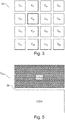
- Figure 3 shows a plurality of capacitive sensing plates arranged in a matrix structure 30.
- the matrix structure 30 is shown to comprise a total of 16 sensing plates C11-C44 arranged in four rows and four columns. It is emphasized that, depending on the specific application, the number of sensing plates may be significantly higher.
- the capacitance between a sense plate in the matrix structure 30 and a conductive object may, as also discussed above, be indicative of the surface topology of the conductive object. In other words, by performing separate capacitance measurements involving all sense caps of the sensing matrix 30, the resulting capacitance measurement results may be indicative of the topology of the conductive object. This relationship may be utilized to obtain a scan of the surface of a three-dimensional conductive object, such as e.g. a human finger.
- Figure 4 shows a principal diagram of a device 40 for measuring a capacitance C S .
- the device 40 is a switched capacitor integrator comprising an operational transconductance amplifier (OTA) 41 which may be utilized to convert the capacitance C S developing between a sense cap and the surface of the conductive object into an output voltage V out indicative of the capacitance C S .
- the output voltage V out may be converted by means of an analog-to-digital converter 42 into a computer readable representation 43 indicative of the measured capacitance.
- OTA operational transconductance amplifier
- V out V ref ⁇ 1 + C s C int
- sample and hold switch 47 is closed and the output voltage is converted by ADC 42 and output as a digital value 43.
- the coupling impedances 18 and 22 mainly comprise capacitive and ohmic components with resistances below 5kOhm and have much lower impedances than the capacitor C s .
- the common mode noise source 48 may be directly coupled between the surface of the conductive object (i.e. the bottom plate of capacitor C s ) and the sense cap electrode (i.e. the top plate of capacitor C s ).
- the common mode noise may be regarded as static (pseudo-static) during one sampling (integration) interval. This means that during one sampling interval, the common mode noise 48 may, as shown in Figure 4 , be constituted by a DC voltage V CMN_DC .
- the voltage V CMN_DC may have a similar effect as a pre-charge being stored on capacitor C s , thus causing a false integration voltage that may be misinterpreted as a wrong capacitance value.
- V CMN_DC As the voltage V CMN_DC is unknown, it needs to be eliminated from the capacitance measurement result.
- To eliminate V CMN_DC it is required to establish a linear equation system with V CMN_DC and C s as independent variables. To solve this equation system, two equations (corresponding to two measurements) are required.
- V CMN_DC There may be at least two options to eliminate the voltage V CMN_DC .
- Prior art proposes to superimpose the voltage V CMN_DC by a two-level DC-drive voltage V DRIVE combined with double correlated sampling of the output signal.
- a drawback of this approach is that the voltage V CMN_DC will most likely change between two sam3ple moments.
- each sense plate such as sense plate C22 shown in Figure 3
- Figure 5 shows such a capacitive sensing plate C22 comprising two sub-plates, i.e. a first sub-plate C22a and a second sub-plate C22b, which are electrically separated by a small gap 35.
- the capacitance for each sub-plate C22a, C22b may be measured simultaneously by two separate integrators, each integrator corresponding to the one shown in Figure 4 .
- V out V ref + V ref ⁇ V CMN DC ⁇ D s 2 ⁇ C int
- V out V ref ⁇ 1 + C s 2 ⁇ C int ⁇ V CMN DC ⁇ C s 2 ⁇ C int
- V out 1 V ref 1 ⁇ 1 + C s 2 ⁇ C int ⁇ V CMN DC ⁇ C s 2 ⁇ C int
- V out 2 V ref 2 ⁇ 1 + C s 2 ⁇ C int ⁇ V CMN DC ⁇ C s 2 ⁇ C int
- V out 1 ⁇ V out 2 V ref 1 ⁇ V ref 2 ⁇ 1 + C s 2 ⁇ C int
- V CMN_DC common mode voltage component
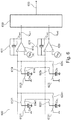
- Figure 6 shows a circuit diagram of an apparatus 600 for measuring capacitances in accordance with an exemplary embodiment. More specifically, the apparatus 600 comprises a first integrator, a second integrator, switching circuitry, and output circuitry 630 for providing a digital output signal 633 indicative of a measured capacitance, i.e. a capacitance formed by one of a plurality of pairs of sub-plates Ca1, Cb1, ... Cai, Cbi, where each pair of sub-plates form a split sense plate as shown in Figure 5 , and a counter plate (not shown). It may be further noted, that the larger the number i may be made, the smaller the impact of the counter electrode's shape variation and/or the counter electrode's distance variation on Cai and Cib will be.
- a measured capacitance i.e. a capacitance formed by one of a plurality of pairs of sub-plates Ca1, Cb1, ... Cai, Cbi, where each pair of sub-plates form a split sense plate as shown in
- the first integrator comprises a first operational transconductance amplifier 610 and a first integrator capacitor C int1 coupled between the inverting input of the first OTA 610 and the output Vout 1 of the first OTA 610.
- a first reference voltage Vref 1 is applied to the non-inverting input of the first OTA 610.
- the second integrator comprises a second OTA 620 and a second integrator capacitor C int2 coupled between the inverting input of the second OTA 620 and the output Vout 2 of the second OTA 620.
- a second reference voltage Vref 2 is applied to the non-inverting input of the second OTA 620.
- the second reference voltage Vref 2 differs from the first reference voltage Vref 1 .
- the switching circuitry comprises switches 611 and 621 for discharging the respective integrator capacitors C int1 and C int2 , switches 6121 to 612i and 6221 to 622i for grounding the respective sub-plates in order to discharge the corresponding capacitors, and switches 6131 to 613i, 6141 to 614i, 6231 to 623i, and 6241 to 624i for selectively coupling the sub-plates to either the inverting input of the first OTA 610 or the inverting input of the second OTA 620.
- the various switches of the switching circuitry are operated in accordance with a number of control signals, which will be discussed in further detail below.
- the output circuitry 630 receives the first output voltage Vout 1 and the second output voltage Vout 2 , performs a sample and hold operation, a subtraction operation and an analog to digital conversion in order to generate the digital output signal 633 based on the differences Vout 2 - Vout 1 and Vref 2 - Vref 1 as discussed above.
- control signal 703 controls the switches 612 and 622 corresponding to the selected pair of capacitors, e.g.
- control signal 705 is activated and closes switches 6141 and 6241 such that the sense plate of capacitor Ca1 is now connected to the inverting input of the second OTA 620 and the sense plate of capacitor Cb1 is connected to the inverting input of the first OTA 610.
- Figure 8 shows a capacitive sensing plate comprising two groups of sub-plates in accordance with an embodiment. More specifically, the first sub-plate Ca is split into eight sub-sub-plates Ca 1 , Ca 2 , Ca 3 , Ca 4 , Ca 5 , Ca 6 , Ca 7 , and Ca 8 which are spatially separated but electrically interconnected. Similarly, the second sub-plate Cb is split into eight sub-sub-plates Cb 1 , Cb 2 , Cb 3 , Cb 4 , Cb 5 , Cb 6 , Cb 7 , and Cb 8 which are also spatially separated but electrically interconnected.
- the sub-sub-plates are arranged in a matrix structure in such a way that the neighbors (in both rows and columns) belong to the other group of sub-sub-plates.
- the averaging resulting from this structure may help to improve the precision of the measurement result even further.
- Figure 11 shows a diagram of circuitry for generating reference voltages Vref 1 and Vref 2 in accordance with another embodiment, which is also in line with the principle discussed above in conjunction with Figure 9 . More specifically, two voltage sources 1141 and 1143 with voltages of respectively V CC and Vref, and a voltage divider comprising resistors R1 and R2 are used. Both the first reference voltage Vref 1 and the second reference voltage Vref 2 are derived from the divided voltage between R1 and R2. More specifically, the second reference voltage Vref 2 is taken directly from the divided voltage, i.e.
- Vref 2 R 1 /(R 1 +R 2 )*V CC
Landscapes
- Engineering & Computer Science (AREA)
- Physics & Mathematics (AREA)
- General Physics & Mathematics (AREA)
- Human Computer Interaction (AREA)
- Multimedia (AREA)
- Theoretical Computer Science (AREA)
- Measurement Of Resistance Or Impedance (AREA)
- Measurement Of Length, Angles, Or The Like Using Electric Or Magnetic Means (AREA)
Priority Applications (3)
| Application Number | Priority Date | Filing Date | Title |
|---|---|---|---|
| EP18210556.9A EP3663779B1 (fr) | 2018-12-05 | 2018-12-05 | Appareil et procédé pour mesurer une capacité et capteur d'empreintes digitales l'utilisant |
| US16/687,955 US10990785B2 (en) | 2018-12-05 | 2019-11-19 | Apparatus and method for measuring a capacitance, and a fingerprint sensor utilizing the same |
| CN201911237665.3A CN111273088B (zh) | 2018-12-05 | 2019-12-05 | 用于测量电容的设备和方法及用所述设备和方法的传感器 |
Applications Claiming Priority (1)
| Application Number | Priority Date | Filing Date | Title |
|---|---|---|---|
| EP18210556.9A EP3663779B1 (fr) | 2018-12-05 | 2018-12-05 | Appareil et procédé pour mesurer une capacité et capteur d'empreintes digitales l'utilisant |
Publications (2)
| Publication Number | Publication Date |
|---|---|
| EP3663779A1 true EP3663779A1 (fr) | 2020-06-10 |
| EP3663779B1 EP3663779B1 (fr) | 2021-10-06 |
Family
ID=64650155
Family Applications (1)
| Application Number | Title | Priority Date | Filing Date |
|---|---|---|---|
| EP18210556.9A Active EP3663779B1 (fr) | 2018-12-05 | 2018-12-05 | Appareil et procédé pour mesurer une capacité et capteur d'empreintes digitales l'utilisant |
Country Status (3)
| Country | Link |
|---|---|
| US (1) | US10990785B2 (fr) |
| EP (1) | EP3663779B1 (fr) |
| CN (1) | CN111273088B (fr) |
Families Citing this family (4)
| Publication number | Priority date | Publication date | Assignee | Title |
|---|---|---|---|---|
| EP3661148B1 (fr) | 2018-11-28 | 2023-05-24 | Nxp B.V. | Procédé d'authentification référencé par l'emplacement et l'identité et système de communication |
| EP3663779B1 (fr) * | 2018-12-05 | 2021-10-06 | Nxp B.V. | Appareil et procédé pour mesurer une capacité et capteur d'empreintes digitales l'utilisant |
| KR102910278B1 (ko) * | 2019-08-09 | 2026-01-09 | 삼성디스플레이 주식회사 | 터치 구동 회로 및 이를 포함하는 표시 장치 |
| CN113257184B (zh) | 2021-05-10 | 2022-10-25 | 京东方科技集团股份有限公司 | 采样电路及驱动方法、像素采样电路、显示装置 |
Citations (7)
| Publication number | Priority date | Publication date | Assignee | Title |
|---|---|---|---|---|
| WO2015133773A1 (fr) * | 2014-03-01 | 2015-09-11 | 주식회사 센트론 | Circuit de détection de saisie tactile de type capacitif |
| US20150338952A1 (en) * | 2014-05-23 | 2015-11-26 | Apple Inc. | Coded integration of a self-capacitance array |
| US20160011014A1 (en) * | 2014-07-11 | 2016-01-14 | Em Microelectronic-Marin Sa | Electronic measurement circuit |
| US9310953B1 (en) * | 2014-11-25 | 2016-04-12 | Cypress Semiconductor Corporation | Full-wave synchronous rectification for self-capacitance sensing |
| US9372582B2 (en) * | 2012-04-19 | 2016-06-21 | Atmel Corporation | Self-capacitance measurement |
| US20160379032A1 (en) * | 2014-01-14 | 2016-12-29 | Focaltech Electronics, Ltd. | Electric field-type fingerprint identification apparatus and state control method and prosthesis identification method thereof |
| KR101715630B1 (ko) * | 2016-04-14 | 2017-03-22 | 주식회사 지니틱스 | 두 개의 피드백 커패시터 간의 피드백 연결 전환을 이용하여 터치입력을 감지하는 방법 및 이를 위한 장치 |
Family Cites Families (30)
| Publication number | Priority date | Publication date | Assignee | Title |
|---|---|---|---|---|
| CA1283452C (fr) * | 1988-03-03 | 1991-04-23 | Miran Milkovic | Circuit differentiel double pente a condensateurs commutes pour wattheuremetre |
| US5841310A (en) * | 1997-04-08 | 1998-11-24 | Burr-Brown Corporation | Current-to-voltage integrator for analog-to-digital converter, and method |
| EP1766547B1 (fr) | 2004-06-18 | 2008-11-19 | Fingerprint Cards AB | Element de capteur d'empreinte digitale |
| JP4586618B2 (ja) | 2005-04-18 | 2010-11-24 | ソニー株式会社 | 人体通信システム及び通信装置 |
| US7460697B2 (en) | 2005-07-19 | 2008-12-02 | Validity Sensors, Inc. | Electronic fingerprint sensor with differential noise cancellation |
| DE602006015160D1 (de) * | 2006-03-15 | 2010-08-12 | Em Microelectronic Marin Sa | Elektronischer Schnittstellenschaltkreis eines kapazitiven Sensors zur Messung eines physikalischen Parameters und Verfahren zur Ingangsetzung des elektronischen Schaltkreises |
| CN101487863B (zh) * | 2008-01-15 | 2011-11-02 | 财团法人交大思源基金会 | 利用数字激发信号来准确测量放大器开路增益的装置 |
| CH700376A2 (de) * | 2009-02-11 | 2010-08-13 | Baumer Innotec Ag | Kapazitiver Sensor und Verfahren zur kapazitiven Erfassung eines Objektabstandes. |
| US8854107B2 (en) * | 2010-05-04 | 2014-10-07 | Zinitix Co., Ltd. | Integrator circuit with inverting integrator and non-inverting integrator |
| JP2012124779A (ja) * | 2010-12-09 | 2012-06-28 | Panasonic Corp | 信号増幅回路 |
| US9754097B2 (en) | 2014-02-21 | 2017-09-05 | Liveensure, Inc. | Method for peer to peer mobile context authentication |
| EP2930851B1 (fr) * | 2014-04-09 | 2018-09-12 | Ams Ag | Convertisseur de numériseur de capacités et procédé pour fournir un signal de sortie numérique |
| US9519819B2 (en) | 2014-07-14 | 2016-12-13 | Fingerprint Cards Ab | Method and electronic device for noise mitigation |
| EP3059553B1 (fr) * | 2015-02-23 | 2018-05-02 | EM Microelectronic-Marin SA | Circuit électronique de mesure |
| US9380208B1 (en) * | 2015-04-13 | 2016-06-28 | Omnivision Technologies, Inc. | Image sensor power supply rejection ratio noise reduction through ramp generator |
| EP3093653B1 (fr) * | 2015-05-13 | 2018-09-26 | ams AG | Circuit de capteur et procédé pour mesurer une grandeur physique ou chimique |
| TWI566120B (zh) * | 2015-05-21 | 2017-01-11 | 速博思股份有限公司 | 具有反射遮蔽電極之生物辨識裝置及其偵測控制方法 |
| CN107003347B (zh) * | 2015-10-23 | 2019-12-17 | 深圳市汇顶科技股份有限公司 | 电容检测传感器及其相关装置和系统 |
| US10311279B2 (en) * | 2016-10-21 | 2019-06-04 | Novatek Microelectronics Corp. | Fingerprint sensor device and operation method thereof |
| EP3327612A1 (fr) | 2016-11-24 | 2018-05-30 | Nxp B.V. | Système et procédé de détection d'empreintes |
| EP3358496B1 (fr) * | 2017-02-02 | 2021-04-07 | Nxp B.V. | Système et procédé de traitement d'empreinte digitale |
| EP3401835A1 (fr) * | 2017-05-12 | 2018-11-14 | Nxp B.V. | Module de détecteur d'empreintes digitales |
| CN108985150B (zh) * | 2017-05-31 | 2022-05-27 | 联咏科技股份有限公司 | 电容式图像传感器 |
| US10205895B2 (en) * | 2017-07-05 | 2019-02-12 | Sunasic Technologies Limited | Capacitive image sensor with noise reduction feature and method operating the same |
| EP3514553B1 (fr) * | 2017-11-20 | 2020-08-05 | Shenzhen Goodix Technology Co., Ltd. | Circuit différentiel, circuit de détection de capacité, appareil de détection tactile et dispositif terminal |
| EP3511860B1 (fr) * | 2018-01-11 | 2024-09-11 | Nxp B.V. | Dispositif de détection d'empreintes digitales avec protection contre les décharges électrostatiques |
| EP3543897A1 (fr) * | 2018-03-19 | 2019-09-25 | Nxp B.V. | Dispositif de détection d'empreintes digitales |
| EP3633393B1 (fr) * | 2018-10-02 | 2023-09-06 | ams AG | Convertisseur capacitance-numerique, interface de capteur intégrée et dispositif de capteur |
| EP3663779B1 (fr) * | 2018-12-05 | 2021-10-06 | Nxp B.V. | Appareil et procédé pour mesurer une capacité et capteur d'empreintes digitales l'utilisant |
| KR102751666B1 (ko) * | 2018-12-27 | 2025-01-10 | 주식회사 엘엑스세미콘 | 전류구동방식의 터치센싱장치 및 터치센싱장치 구동방법 |
-
2018
- 2018-12-05 EP EP18210556.9A patent/EP3663779B1/fr active Active
-
2019
- 2019-11-19 US US16/687,955 patent/US10990785B2/en active Active
- 2019-12-05 CN CN201911237665.3A patent/CN111273088B/zh active Active
Patent Citations (7)
| Publication number | Priority date | Publication date | Assignee | Title |
|---|---|---|---|---|
| US9372582B2 (en) * | 2012-04-19 | 2016-06-21 | Atmel Corporation | Self-capacitance measurement |
| US20160379032A1 (en) * | 2014-01-14 | 2016-12-29 | Focaltech Electronics, Ltd. | Electric field-type fingerprint identification apparatus and state control method and prosthesis identification method thereof |
| WO2015133773A1 (fr) * | 2014-03-01 | 2015-09-11 | 주식회사 센트론 | Circuit de détection de saisie tactile de type capacitif |
| US20150338952A1 (en) * | 2014-05-23 | 2015-11-26 | Apple Inc. | Coded integration of a self-capacitance array |
| US20160011014A1 (en) * | 2014-07-11 | 2016-01-14 | Em Microelectronic-Marin Sa | Electronic measurement circuit |
| US9310953B1 (en) * | 2014-11-25 | 2016-04-12 | Cypress Semiconductor Corporation | Full-wave synchronous rectification for self-capacitance sensing |
| KR101715630B1 (ko) * | 2016-04-14 | 2017-03-22 | 주식회사 지니틱스 | 두 개의 피드백 커패시터 간의 피드백 연결 전환을 이용하여 터치입력을 감지하는 방법 및 이를 위한 장치 |
Also Published As
| Publication number | Publication date |
|---|---|
| US10990785B2 (en) | 2021-04-27 |
| CN111273088B (zh) | 2024-06-21 |
| CN111273088A (zh) | 2020-06-12 |
| EP3663779B1 (fr) | 2021-10-06 |
| US20200184175A1 (en) | 2020-06-11 |
Similar Documents
| Publication | Publication Date | Title |
|---|---|---|
| US10990785B2 (en) | Apparatus and method for measuring a capacitance, and a fingerprint sensor utilizing the same | |
| US6583632B2 (en) | Method of determining very small capacitances | |
| US8854059B2 (en) | Embedded SAR based active gain capacitance measurement system and method | |
| US8228076B2 (en) | Deconvolution-based capacitive touch detection circuit and method | |
| CN105391449B (zh) | 用于多个电极的采样电路和采样方法 | |
| CN107690584B (zh) | 电容检测电路、电容检测的方法、触摸检测装置和终端设备 | |
| US20170139540A1 (en) | Analog Elimination of Ungrounded Conductive Objects in Capacitive Sensing | |
| US20130106779A1 (en) | Noise compensation techniques for capacitive touch screen systems | |
| US20100231241A1 (en) | Capacitance measurement system and method | |
| KR20130136357A (ko) | 터치 검출 장치 | |
| KR20150060565A (ko) | 근접 검출을 위한 용량성 감지 인터페이스 | |
| CN112795476B (zh) | 纳米孔测序电路、测序方法及装置 | |
| CN109496273A (zh) | 电容检测电路、触摸检测装置和终端设备 | |
| CN109645978B (zh) | 一种脑部探针读出电路 | |
| Nojdelov et al. | Capacitive-sensor interface with high accuracy and stability | |
| US4086541A (en) | Time division multiplexing amplifier | |
| US5519328A (en) | Compensation for dielectric absorption effect | |
| CN119178928A (zh) | 一种宽带微弱电流信号检测系统及检测方法 | |
| US20230266371A1 (en) | Impedance measurement | |
| Watanabe et al. | A switched-capacitor digital capacitance bridge | |
| JPH0131967Y2 (fr) | ||
| JPH0119107Y2 (fr) | ||
| KR20210101977A (ko) | 지문 감지 장치 및 그 방법 | |
| US20040124857A1 (en) | Capacitive measurement device | |
| Matsumoto et al. | A switched-capacitor digital capacitance meter |
Legal Events
| Date | Code | Title | Description |
|---|---|---|---|
| PUAI | Public reference made under article 153(3) epc to a published international application that has entered the european phase |
Free format text: ORIGINAL CODE: 0009012 |
|
| STAA | Information on the status of an ep patent application or granted ep patent |
Free format text: STATUS: THE APPLICATION HAS BEEN PUBLISHED |
|
| AK | Designated contracting states |
Kind code of ref document: A1 Designated state(s): AL AT BE BG CH CY CZ DE DK EE ES FI FR GB GR HR HU IE IS IT LI LT LU LV MC MK MT NL NO PL PT RO RS SE SI SK SM TR |
|
| AX | Request for extension of the european patent |
Extension state: BA ME |
|
| STAA | Information on the status of an ep patent application or granted ep patent |
Free format text: STATUS: REQUEST FOR EXAMINATION WAS MADE |
|
| 17P | Request for examination filed |
Effective date: 20201210 |
|
| RBV | Designated contracting states (corrected) |
Designated state(s): AL AT BE BG CH CY CZ DE DK EE ES FI FR GB GR HR HU IE IS IT LI LT LU LV MC MK MT NL NO PL PT RO RS SE SI SK SM TR |
|
| GRAP | Despatch of communication of intention to grant a patent |
Free format text: ORIGINAL CODE: EPIDOSNIGR1 |
|
| STAA | Information on the status of an ep patent application or granted ep patent |
Free format text: STATUS: GRANT OF PATENT IS INTENDED |
|
| INTG | Intention to grant announced |
Effective date: 20210624 |
|
| GRAS | Grant fee paid |
Free format text: ORIGINAL CODE: EPIDOSNIGR3 |
|
| GRAA | (expected) grant |
Free format text: ORIGINAL CODE: 0009210 |
|
| STAA | Information on the status of an ep patent application or granted ep patent |
Free format text: STATUS: THE PATENT HAS BEEN GRANTED |
|
| AK | Designated contracting states |
Kind code of ref document: B1 Designated state(s): AL AT BE BG CH CY CZ DE DK EE ES FI FR GB GR HR HU IE IS IT LI LT LU LV MC MK MT NL NO PL PT RO RS SE SI SK SM TR |
|
| REG | Reference to a national code |
Ref country code: GB Ref legal event code: FG4D |
|
| REG | Reference to a national code |
Ref country code: CH Ref legal event code: EP Ref country code: AT Ref legal event code: REF Ref document number: 1436660 Country of ref document: AT Kind code of ref document: T Effective date: 20211015 |
|
| REG | Reference to a national code |
Ref country code: IE Ref legal event code: FG4D |
|
| REG | Reference to a national code |
Ref country code: DE Ref legal event code: R096 Ref document number: 602018024579 Country of ref document: DE |
|
| REG | Reference to a national code |
Ref country code: LT Ref legal event code: MG9D |
|
| REG | Reference to a national code |
Ref country code: NL Ref legal event code: MP Effective date: 20211006 |
|
| REG | Reference to a national code |
Ref country code: AT Ref legal event code: MK05 Ref document number: 1436660 Country of ref document: AT Kind code of ref document: T Effective date: 20211006 |
|
| PG25 | Lapsed in a contracting state [announced via postgrant information from national office to epo] |
Ref country code: RS Free format text: LAPSE BECAUSE OF FAILURE TO SUBMIT A TRANSLATION OF THE DESCRIPTION OR TO PAY THE FEE WITHIN THE PRESCRIBED TIME-LIMIT Effective date: 20211006 Ref country code: LT Free format text: LAPSE BECAUSE OF FAILURE TO SUBMIT A TRANSLATION OF THE DESCRIPTION OR TO PAY THE FEE WITHIN THE PRESCRIBED TIME-LIMIT Effective date: 20211006 Ref country code: FI Free format text: LAPSE BECAUSE OF FAILURE TO SUBMIT A TRANSLATION OF THE DESCRIPTION OR TO PAY THE FEE WITHIN THE PRESCRIBED TIME-LIMIT Effective date: 20211006 Ref country code: BG Free format text: LAPSE BECAUSE OF FAILURE TO SUBMIT A TRANSLATION OF THE DESCRIPTION OR TO PAY THE FEE WITHIN THE PRESCRIBED TIME-LIMIT Effective date: 20220106 Ref country code: AT Free format text: LAPSE BECAUSE OF FAILURE TO SUBMIT A TRANSLATION OF THE DESCRIPTION OR TO PAY THE FEE WITHIN THE PRESCRIBED TIME-LIMIT Effective date: 20211006 |
|
| PG25 | Lapsed in a contracting state [announced via postgrant information from national office to epo] |
Ref country code: IS Free format text: LAPSE BECAUSE OF FAILURE TO SUBMIT A TRANSLATION OF THE DESCRIPTION OR TO PAY THE FEE WITHIN THE PRESCRIBED TIME-LIMIT Effective date: 20220206 Ref country code: SE Free format text: LAPSE BECAUSE OF FAILURE TO SUBMIT A TRANSLATION OF THE DESCRIPTION OR TO PAY THE FEE WITHIN THE PRESCRIBED TIME-LIMIT Effective date: 20211006 Ref country code: PT Free format text: LAPSE BECAUSE OF FAILURE TO SUBMIT A TRANSLATION OF THE DESCRIPTION OR TO PAY THE FEE WITHIN THE PRESCRIBED TIME-LIMIT Effective date: 20220207 Ref country code: PL Free format text: LAPSE BECAUSE OF FAILURE TO SUBMIT A TRANSLATION OF THE DESCRIPTION OR TO PAY THE FEE WITHIN THE PRESCRIBED TIME-LIMIT Effective date: 20211006 Ref country code: NO Free format text: LAPSE BECAUSE OF FAILURE TO SUBMIT A TRANSLATION OF THE DESCRIPTION OR TO PAY THE FEE WITHIN THE PRESCRIBED TIME-LIMIT Effective date: 20220106 Ref country code: NL Free format text: LAPSE BECAUSE OF FAILURE TO SUBMIT A TRANSLATION OF THE DESCRIPTION OR TO PAY THE FEE WITHIN THE PRESCRIBED TIME-LIMIT Effective date: 20211006 Ref country code: LV Free format text: LAPSE BECAUSE OF FAILURE TO SUBMIT A TRANSLATION OF THE DESCRIPTION OR TO PAY THE FEE WITHIN THE PRESCRIBED TIME-LIMIT Effective date: 20211006 Ref country code: HR Free format text: LAPSE BECAUSE OF FAILURE TO SUBMIT A TRANSLATION OF THE DESCRIPTION OR TO PAY THE FEE WITHIN THE PRESCRIBED TIME-LIMIT Effective date: 20211006 Ref country code: GR Free format text: LAPSE BECAUSE OF FAILURE TO SUBMIT A TRANSLATION OF THE DESCRIPTION OR TO PAY THE FEE WITHIN THE PRESCRIBED TIME-LIMIT Effective date: 20220107 Ref country code: ES Free format text: LAPSE BECAUSE OF FAILURE TO SUBMIT A TRANSLATION OF THE DESCRIPTION OR TO PAY THE FEE WITHIN THE PRESCRIBED TIME-LIMIT Effective date: 20211006 |
|
| REG | Reference to a national code |
Ref country code: DE Ref legal event code: R097 Ref document number: 602018024579 Country of ref document: DE |
|
| PG25 | Lapsed in a contracting state [announced via postgrant information from national office to epo] |
Ref country code: SM Free format text: LAPSE BECAUSE OF FAILURE TO SUBMIT A TRANSLATION OF THE DESCRIPTION OR TO PAY THE FEE WITHIN THE PRESCRIBED TIME-LIMIT Effective date: 20211006 Ref country code: SK Free format text: LAPSE BECAUSE OF FAILURE TO SUBMIT A TRANSLATION OF THE DESCRIPTION OR TO PAY THE FEE WITHIN THE PRESCRIBED TIME-LIMIT Effective date: 20211006 Ref country code: RO Free format text: LAPSE BECAUSE OF FAILURE TO SUBMIT A TRANSLATION OF THE DESCRIPTION OR TO PAY THE FEE WITHIN THE PRESCRIBED TIME-LIMIT Effective date: 20211006 Ref country code: MC Free format text: LAPSE BECAUSE OF FAILURE TO SUBMIT A TRANSLATION OF THE DESCRIPTION OR TO PAY THE FEE WITHIN THE PRESCRIBED TIME-LIMIT Effective date: 20211006 Ref country code: EE Free format text: LAPSE BECAUSE OF FAILURE TO SUBMIT A TRANSLATION OF THE DESCRIPTION OR TO PAY THE FEE WITHIN THE PRESCRIBED TIME-LIMIT Effective date: 20211006 Ref country code: DK Free format text: LAPSE BECAUSE OF FAILURE TO SUBMIT A TRANSLATION OF THE DESCRIPTION OR TO PAY THE FEE WITHIN THE PRESCRIBED TIME-LIMIT Effective date: 20211006 Ref country code: CZ Free format text: LAPSE BECAUSE OF FAILURE TO SUBMIT A TRANSLATION OF THE DESCRIPTION OR TO PAY THE FEE WITHIN THE PRESCRIBED TIME-LIMIT Effective date: 20211006 |
|
| REG | Reference to a national code |
Ref country code: CH Ref legal event code: PL |
|
| PLBE | No opposition filed within time limit |
Free format text: ORIGINAL CODE: 0009261 |
|
| STAA | Information on the status of an ep patent application or granted ep patent |
Free format text: STATUS: NO OPPOSITION FILED WITHIN TIME LIMIT |
|
| 26N | No opposition filed |
Effective date: 20220707 |
|
| REG | Reference to a national code |
Ref country code: BE Ref legal event code: MM Effective date: 20211231 |
|
| PG25 | Lapsed in a contracting state [announced via postgrant information from national office to epo] |
Ref country code: LU Free format text: LAPSE BECAUSE OF NON-PAYMENT OF DUE FEES Effective date: 20211205 Ref country code: IE Free format text: LAPSE BECAUSE OF NON-PAYMENT OF DUE FEES Effective date: 20211205 Ref country code: AL Free format text: LAPSE BECAUSE OF FAILURE TO SUBMIT A TRANSLATION OF THE DESCRIPTION OR TO PAY THE FEE WITHIN THE PRESCRIBED TIME-LIMIT Effective date: 20211006 |
|
| PG25 | Lapsed in a contracting state [announced via postgrant information from national office to epo] |
Ref country code: SI Free format text: LAPSE BECAUSE OF FAILURE TO SUBMIT A TRANSLATION OF THE DESCRIPTION OR TO PAY THE FEE WITHIN THE PRESCRIBED TIME-LIMIT Effective date: 20211006 Ref country code: BE Free format text: LAPSE BECAUSE OF NON-PAYMENT OF DUE FEES Effective date: 20211231 |
|
| PG25 | Lapsed in a contracting state [announced via postgrant information from national office to epo] |
Ref country code: LI Free format text: LAPSE BECAUSE OF NON-PAYMENT OF DUE FEES Effective date: 20211231 Ref country code: CH Free format text: LAPSE BECAUSE OF NON-PAYMENT OF DUE FEES Effective date: 20211231 |
|
| PG25 | Lapsed in a contracting state [announced via postgrant information from national office to epo] |
Ref country code: IT Free format text: LAPSE BECAUSE OF FAILURE TO SUBMIT A TRANSLATION OF THE DESCRIPTION OR TO PAY THE FEE WITHIN THE PRESCRIBED TIME-LIMIT Effective date: 20211006 |
|
| PG25 | Lapsed in a contracting state [announced via postgrant information from national office to epo] |
Ref country code: CY Free format text: LAPSE BECAUSE OF FAILURE TO SUBMIT A TRANSLATION OF THE DESCRIPTION OR TO PAY THE FEE WITHIN THE PRESCRIBED TIME-LIMIT Effective date: 20211006 |
|
| PG25 | Lapsed in a contracting state [announced via postgrant information from national office to epo] |
Ref country code: HU Free format text: LAPSE BECAUSE OF FAILURE TO SUBMIT A TRANSLATION OF THE DESCRIPTION OR TO PAY THE FEE WITHIN THE PRESCRIBED TIME-LIMIT; INVALID AB INITIO Effective date: 20181205 |
|
| GBPC | Gb: european patent ceased through non-payment of renewal fee |
Effective date: 20221205 |
|
| P01 | Opt-out of the competence of the unified patent court (upc) registered |
Effective date: 20230725 |
|
| PG25 | Lapsed in a contracting state [announced via postgrant information from national office to epo] |
Ref country code: GB Free format text: LAPSE BECAUSE OF NON-PAYMENT OF DUE FEES Effective date: 20221205 |
|
| PG25 | Lapsed in a contracting state [announced via postgrant information from national office to epo] |
Ref country code: MK Free format text: LAPSE BECAUSE OF FAILURE TO SUBMIT A TRANSLATION OF THE DESCRIPTION OR TO PAY THE FEE WITHIN THE PRESCRIBED TIME-LIMIT Effective date: 20211006 |
|
| PG25 | Lapsed in a contracting state [announced via postgrant information from national office to epo] |
Ref country code: TR Free format text: LAPSE BECAUSE OF FAILURE TO SUBMIT A TRANSLATION OF THE DESCRIPTION OR TO PAY THE FEE WITHIN THE PRESCRIBED TIME-LIMIT Effective date: 20211006 |
|
| PG25 | Lapsed in a contracting state [announced via postgrant information from national office to epo] |
Ref country code: MT Free format text: LAPSE BECAUSE OF FAILURE TO SUBMIT A TRANSLATION OF THE DESCRIPTION OR TO PAY THE FEE WITHIN THE PRESCRIBED TIME-LIMIT Effective date: 20211006 |
|
| PGFP | Annual fee paid to national office [announced via postgrant information from national office to epo] |
Ref country code: DE Payment date: 20251126 Year of fee payment: 8 |
|
| PGFP | Annual fee paid to national office [announced via postgrant information from national office to epo] |
Ref country code: FR Payment date: 20251119 Year of fee payment: 8 |