EP3663985A1 - Herstellungsverfahren einer vorrichtung, die einen körper in form einer karte und eine informationszone umfasst - Google Patents
Herstellungsverfahren einer vorrichtung, die einen körper in form einer karte und eine informationszone umfasst Download PDFInfo
- Publication number
- EP3663985A1 EP3663985A1 EP18306646.3A EP18306646A EP3663985A1 EP 3663985 A1 EP3663985 A1 EP 3663985A1 EP 18306646 A EP18306646 A EP 18306646A EP 3663985 A1 EP3663985 A1 EP 3663985A1
- Authority
- EP
- European Patent Office
- Prior art keywords
- card
- display
- layer
- information
- laser
- Prior art date
- Legal status (The legal status is an assumption and is not a legal conclusion. Google has not performed a legal analysis and makes no representation as to the accuracy of the status listed.)
- Withdrawn
Links
Images


Classifications
-
- B—PERFORMING OPERATIONS; TRANSPORTING
- B42—BOOKBINDING; ALBUMS; FILES; SPECIAL PRINTED MATTER
- B42D—BOOKS; BOOK COVERS; LOOSE LEAVES; PRINTED MATTER CHARACTERISED BY IDENTIFICATION OR SECURITY FEATURES; PRINTED MATTER OF SPECIAL FORMAT OR STYLE NOT OTHERWISE PROVIDED FOR; DEVICES FOR USE THEREWITH AND NOT OTHERWISE PROVIDED FOR; MOVABLE-STRIP WRITING OR READING APPARATUS
- B42D25/00—Information-bearing cards or sheet-like structures characterised by identification or security features; Manufacture thereof
- B42D25/40—Manufacture
- B42D25/405—Marking
- B42D25/41—Marking using electromagnetic radiation
-
- B—PERFORMING OPERATIONS; TRANSPORTING
- B42—BOOKBINDING; ALBUMS; FILES; SPECIAL PRINTED MATTER
- B42D—BOOKS; BOOK COVERS; LOOSE LEAVES; PRINTED MATTER CHARACTERISED BY IDENTIFICATION OR SECURITY FEATURES; PRINTED MATTER OF SPECIAL FORMAT OR STYLE NOT OTHERWISE PROVIDED FOR; DEVICES FOR USE THEREWITH AND NOT OTHERWISE PROVIDED FOR; MOVABLE-STRIP WRITING OR READING APPARATUS
- B42D25/00—Information-bearing cards or sheet-like structures characterised by identification or security features; Manufacture thereof
- B42D25/30—Identification or security features, e.g. for preventing forgery
- B42D25/351—Translucent or partly translucent parts, e.g. windows
-
- G—PHYSICS
- G06—COMPUTING OR CALCULATING; COUNTING
- G06K—GRAPHICAL DATA READING; PRESENTATION OF DATA; RECORD CARRIERS; HANDLING RECORD CARRIERS
- G06K19/00—Record carriers for use with machines and with at least a part designed to carry digital markings
- G06K19/06—Record carriers for use with machines and with at least a part designed to carry digital markings characterised by the kind of the digital marking, e.g. shape, nature, code
- G06K19/067—Record carriers with conductive marks, printed circuits or semiconductor circuit elements, e.g. credit or identity cards also with resonating or responding marks without active components
- G06K19/07—Record carriers with conductive marks, printed circuits or semiconductor circuit elements, e.g. credit or identity cards also with resonating or responding marks without active components with integrated circuit chips
- G06K19/0723—Record carriers with conductive marks, printed circuits or semiconductor circuit elements, e.g. credit or identity cards also with resonating or responding marks without active components with integrated circuit chips the record carrier comprising an arrangement for non-contact communication, e.g. wireless communication circuits on transponder cards, non-contact smart cards or RFIDs
-
- G—PHYSICS
- G06—COMPUTING OR CALCULATING; COUNTING
- G06K—GRAPHICAL DATA READING; PRESENTATION OF DATA; RECORD CARRIERS; HANDLING RECORD CARRIERS
- G06K19/00—Record carriers for use with machines and with at least a part designed to carry digital markings
- G06K19/06—Record carriers for use with machines and with at least a part designed to carry digital markings characterised by the kind of the digital marking, e.g. shape, nature, code
- G06K19/067—Record carriers with conductive marks, printed circuits or semiconductor circuit elements, e.g. credit or identity cards also with resonating or responding marks without active components
- G06K19/07—Record carriers with conductive marks, printed circuits or semiconductor circuit elements, e.g. credit or identity cards also with resonating or responding marks without active components with integrated circuit chips
- G06K19/077—Constructional details, e.g. mounting of circuits in the carrier
- G06K19/07701—Constructional details, e.g. mounting of circuits in the carrier the record carrier comprising an interface suitable for human interaction
- G06K19/07703—Constructional details, e.g. mounting of circuits in the carrier the record carrier comprising an interface suitable for human interaction the interface being visual
- G06K19/07707—Constructional details, e.g. mounting of circuits in the carrier the record carrier comprising an interface suitable for human interaction the interface being visual the visual interface being a display, e.g. LCD or electronic ink
Definitions
- the invention relates to a method for manufacturing a device comprising a card-shaped body and an information area with numbers or information visible from the outside.
- the device can typically be a chip card, in particular a bank card, or a biometric card.
- the invention also relates to a method of manufacturing a card comprising graphic patterns visible on the surface of the card body.
- the patterns generally include geometric shapes in two or even three dimensions or alphanumeric characters, on a card body.
- the patterns can for example be produced by printing, in particular by material jet or screen printing.
- the invention finds application in particular in bank cards comprising at least one surface reserved for embossing according to a standard of bank chip cards. It can also find application in bank cards conforming to the standard of flat bank cards (not embossed).
- the invention may relate to devices in the form of a card and / or chip, with layers or laminated sheets such as identity cards or passports, badges or loyalty, health or access cards. or transportation.
- the invention can also relate to the personalization or marking of smart cards in general with personalization patterns (distinct from characters or alphanumeric data (company logos, drawings, etc.)
- Bank cards include a standardized embossing area to receive bank personalization data such as a bank number, an expiration date, in the form of embossing.
- Embossing consists of punching the card with a punch comprising a character (or geometric pattern) to be reproduced on the card.
- One side of the card has the intaglio character / pattern and the other opposite side has the same raised character protruding from the surface of the card.
- the method of embossing the numbers in relief as we know it at present is very restrictive at the manufacturing level. Indeed, the embossing area must be clear of all electronics (so as not to damage it during the embossing process in relief), and this embossing area must be excluded from the graphic printing area of the map.
- this embossing zone limits the positioning of the components, their size, the positioning of the antenna to avoid a possible cut-off (and therefore its electronic properties or radio frequency communication performance), the visual appearance of the card, etc ...
- the graphics card has a display screen, which can be activated with the buttons on the body of the card.
- This card allows the user to view the account balance, or generate a single use number (OTP) for online purchases.
- OTP single use number
- This card may include a biometric sensor to improve security (when the owner puts his finger on the sensor, the card number is displayed on the screen).
- biometric sensor when the owner puts his finger on the sensor, the card number is displayed on the screen.
- This solution is quite restrictive regarding the design of the card.
- the screen can be quite bulky and unsightly.
- the inventors thought to solve the problems associated with embossing by simply printing the numbers on the body of the card, but it would be less effective in terms of security (much easier to reproduce for fraud) and the number would always be visible for fraudsters.
- the patent application KR20120044409 (A ) describes a card comprising a screen of the AMOLED (Amorphous Matrix Organic LED) type in English for displaying payment information.
- AMOLED Amorphous Matrix Organic LED
- the patent application US2017289127 (A1 ) describes a function allowing access to the bank card number and / or its cryptogram via biometric authentication on a card sensor.
- the invention proposes to solve all or part of the problems mentioned above.
- Its objective is to solve in particular the problems linked to embossing, to prevent bank fraud and to increase the level of security, while keeping an aesthetic aspect.
- the invention can propose a luminescent card which by default has no visible number;
- the card number can preferably be displayed by an AMOLED strip laminated in the body of the card and activated by a biometric sensor, in particular a fingerprint sensor.
- the card can be powered by a small battery and can be recharged by being connected to a reader with electrical contacts or with an induction charger.
- the battery can also be designed so that its life cycle lasts the necessary time (1 to 3 years)
- the invention can consist in making the screen and / or the numbers disappear when there is no need for display and making them appear when necessary.
- the area devoted to the screen and / or alphanumeric characters has the same visual appearance as the rest of the map area.
- This entire display surface can have the same visual attributes and / or uses as the rest of the card body surface.
- the card can include a layer above the display surface which is translucent (and not transparent) in the absence of a display need.
- the screen and or the characters are not visible.
- the almost total surface of the card has the same visual aspect.
- the card does not have only one or more layer (s) completely made of transparent material to cover the display or the display area.
- the surface of the card is substantially homogeneous between the display area and the area adjacent to the display in the sense that the display area or the screen is not clearly visible through the layer in the absence of active display.
- the rate of translucency or partial light transmission can be determined in particular as a function of the material of the layer and its rate of transmission.
- the rate can also be a function of the light intensity or contrast or dimensions of the characters of the display.
- the external or covering layer of the display and / or of the display area may for example have a thickness of approximately 20 to 100 ⁇ m.
- it can be associated with a transparent layer so as to allow more light to pass through.
- the translucent or partially opaque layer can represent 5 to 95% of the thickness of the covering layer, the rest can be transparent (or vice versa).
- the reserved embossing area to receive a display and display the credit card number.
- the information can be displayed or appear at the desired time on command or user intervention.
- the card may include a graphic personalization pattern which extends at least in part or in whole above the display or above the numbers displayed.
- a graphic personalization pattern which extends at least in part or in whole above the display or above the numbers displayed.
- the display can be bright or contrasted enough to appear on the surface of the card even through a non-transparent cover sheet.
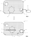
- FIG. 1 Illustrated is a device of the invention, in the form of a bank card 1, obtained by the implementation of a manufacturing method according to a mode of the invention.
- the device (or smart card) 1 comprises a card body 2 and numbers 5 visible on the surface 3 of the body 2 of the device (or card).
- the numbers are here displayed on a display 7 by display on a display 7 of the card, (rather than embossed (or in relief) or be produced by jet printing of material, in particular 2D or 3D as in the prior art.
- the bank card may include an integrated circuit chip module 4 with flush electrical contacts as a communication interface with a contact reader. It can include a radio frequency communication antenna (not shown).
- the card can include, as here, a biometric fingerprint sensor 9.
- the card can include another type of biometric sensor (voice recognition or other). It can include any interface with a user allowing authentication, such as for example a keyboard for entering an identification code. If necessary, the card has just a switch in place of the sensor to trigger the display of the number just at the right time out of sight. The switch can be actuated by a bending sensor such as a piezoelectric sensor.
- the display can be triggered by subjecting the card to an energy source such as an electromagnetic field of an NFC reader.
- the energy source can be a reader with electrical contacts contacting the areas of module 4 of the card and configured to allow reading of the information (transparent reader or not covering the information.
- the card may not include a sensor 9 or a battery 23.
- the numbers referenced 5 form a conventional bank card number.
- the numbers referenced 6 form the expiration date of the bank card. These numbers 5 and 6 are displayed in an area that was reserved or dedicated to embossing in accordance with the EMV bank or payment card standard.
- the surname and first name are normally positioned in the lower part of box 8.
- the display 7 can be placed in a reserved or dedicated area 8 for embossing or for the formation of bank numbers; Zone 8 has a location that complies with a standard for a bank chip card, in particular EMV.
- the display is placed here between the sheets or layers 10 and 11.
- the card here comprises an upper main surface 3 and an opposite surface of standardized thickness equal to 0.78 mm.
- the dimensions preferably corresponding to an ISO 7616 standard for smart cards.
- the targeted cards can have different dimensions from those recommended by the standard, in particular smaller.
- the invention can also target cards obtained by molding / overmolding or injection, or mono or multi-material injection or multi-material co-extrusion. So one of the layers can be different colors. It can optionally include a card body consisting of a layer homogeneous material (except printing and protective layer). In this case, a single layer is embossed. The card can be molded or injected rather than laminated (laminated). It may include a graphic print on the surface, whether or not associated with a varnish or protective layer (overlay).
- the assembly includes upper 10 and lower 13 outer protective layers; It comprises two main layers or sheets of core 11, 12 sandwiched between layers 10 and 13. These layers are generally made of plastic material commonly used in the smart card industry, such as PC, PET, PE, ABS. and PVC.
- the information area Z1 is covered by a layer 10 of material.
- Layer 10 can be configured for partially let in light (being semi-opaque or translucent for example).
- the layer 10 can receive or be configured to receive a personalization or graphic printing extending both in (or on) the information zone Z1 and outside said information zone in (or on) the residual surface of the card-shaped body.
- Components 4 and 9 can also be mounted and connected by inserting in cavities made through layer 10 and other layers such as 11 and 12.
- the various components 7, 4 and 9 can be electrically connected to a thin flexible printed circuit comprising in particular a microprocessor and a battery (not shown).
- the card may preferably include a personalization marking which extends both on the display 7 and on said external main surface 3 of the card body.
- the marking may be a graphic impression such as a uniform background 15 or a pattern 16 such as a star, which extends at least in part or in full on the display 7 or on said displayed numbers 5.
- the display can be formed by any known technology of the smart card. It can advantageously be formed by an AMOLED technique to have in particular brightness and save the battery.
- the print 15, 16 can be printed on one side of the layers 9 or 10 at their interface. If necessary, a protective varnish can cover them. Printing may cover only the edges of the display or all of it. Printing may stop just before covering the numbers. Thus, the non-active areas of the display, generally located a few millimeters (1 - 5 mm) at the edge of the display, can be masked by graphic customization.
- the sheet 10 can be chosen so as to ensure visibility of the numbers displayed through the sheet according to the display technology selected.
- the sheet can be translucent, opaque or semi-opaque.
- the cover or covering sheet may have a light transmission coefficient of between 0.4 and 1.
- the cover or cover sheet 10 can be configured (or include a colored or patterned print on the back), so as to standardize the transparency or opacity of the sheet in order to avoid distinguishing the peripheral delimitation of the display 8.
- a user wishing to carry out a transaction with a bank card number has the smart card 1.
- the card has a module 4 and a biometric sensor.
- the card 1 has a relatively uniform graphic personalization 16 or background on the outer layer 10. It also has a non-uniform graphic personalization (star 15) whose thickness of the contour line is narrower than that of the characters forming the numbers. Thus, despite an overlay, the characters of the numbers remain legible.
- the user presents his finger 19 on the sensor 9 to authenticate.
- a display manager and / or transaction microcontroller of the internal printed circuit card of the card controls the display of the bank card number 5 on the display 7.
- the number appears through the layer 10 and uniform graphic 16 and non-uniform graphic personalization 15.
- the card may not include graphic personalization 16 but be content with a layer of material of color or uniform appearance (neutral or colored) more or less opaque with respect to light reflected on the surface. It can for example comprise a metallic layer, steel, platinum, gold, very fine aluminum of thickness configured so as to allow the passage of light or a layer of natural or synthetic wood of thickness configured so as to allow the passage of the light.
- the light emitted by the AMOLED type diodes passes sufficiently through the layer 10 to be seen by transmission through the layer 10.
- the card may not include any visible component on the surface 3 (component 4 or 9) and have a graphic personalization which covers the entire surface of the card or at least a very large majority.
- the card allows an increase in the area of personalization. It does not interrupt or intersect the image or a personalization reason on the card by the presence of the card numbers.
- the size of the screen 7 preferably covers the area assigned to the number (PAN) or information 5 of the card.
- the central layer 11 may comprise a positioning frame 28 of the printed circuit 26.
- the card here comprises a graphics processing unit 30 making it possible to control a matrix of rows and columns for displaying information or image on the AMOLED display.
- the information is displayed on screen 7 and is visible to an observer (Ob.) Through the transparent layers arranged above the screen.
- the impression of personalization (star 15) or decoration (substantially uniform background 16) can be carried out in particular at the level of the layer 22a so as not to hinder the reading of the information 5.
- FIG 6 illustrates a 1B card configured according to an alternative principle to that of figure 5 .
- the same reference numbers designate elements which are identical or similar from one figure to another.
- the light source may include an LED diode under each series of 4 digits composing the bank card number.
- the personalization information 5, 6, 13 can be produced in particular in two ways below. They can be formed by ablation of material at places corresponding to the information, in the L1 layer. Alternatively, they can be formed in a transparent L2 laser layer by blackening the areas of the L2 laser layer around the information.
- the cards may not include a battery (or capacities) and be supplied by electromagnetic field via an antenna 21.
- the card may include a transparent layer 10c (instead of being partially transparent) and a second laser layer L3 (not shown) disposed above the first laser layer L1, the function of which is to allow blackening by laser preventing visualization with the naked eye under lighting or exposure to natural light external to the card (or device).
- the method can initially provide for the marking by focusing the laser on a first laser layer L1 or L2 and then for carrying out an opacifying or blackening or camouflage marking by scrambling, on the second laser layer L3.
- the card may include a print 22a which provides an effect similar to the second laser layer L3 of masking or scrambling information 5, 6 or even 13.
- L3 laser layers or printing of masking or scrambling or film with controlled opacity can participate together or individually in keeping the information of the device confidential.
- the screen 7 does not need to have a graphics controller 30, an activation command may be sufficient even if it is of the AMOLED type.
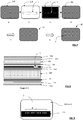
- FIG 8 illustrated is a sectional view AA of the map of the figure 6 .
- the card includes an entirely black or opaque L1 laser layer.
- Information 5 is formed in layer L1 by laser ablation (removal of material).
- the L1 layer may be sensitive to the laser and become transparent or opaque in response to laser activation.
- the card comprises a layer or laser zone L2 which is blackened on a surface R1 extending around the information 5 and with the exception of the information.
- This layer L2 constitutes an alternative to the laser layer L1 of the figure 6 .
- the card can include this type of layer on at least part or all of the surface of the card to cover at least the personalization information 5, 6, 13.
- the layer to be blackened by laser is a rectangular area R1 of the laser overlay 55 ⁇ m thick, substantially covering the display (or screen) or light source.
- the unmarked areas correspond to the numbers to be made visible or displayed on the surface of the card body.
- the AMOLED screen (or display) can light up when the fingerprint reader 9 authenticates the finger 19 of the card user.
- the light can thus pass through the laser layer (or laser overlay) configured as a light filter by the laser marking so as to let only the numbers appear to an observer of the surface of the card.
- the card may include a film with electrically controlled opacity or equivalent.
- This film can be placed between the information marked or displayed on the card and an external surface of the card from which the information is visible, (for example the front face of the card.
- its opacity may decrease so as to reveal the information through the film.
- the method provides for activating the film with controlled opacity to reduce its opacity and allow a laser beam to pass through to a marking layer arranged below.
- the activation of a drop in opacity can be controlled, by an instruction sent by a reader to a microcontroller 30 ( or other) for controlling the opacity by various means including in particular an instruction via the contact pads of the module 4 or via the radiofrequency antenna 21.
- the bank card can alternatively be a device with sheets or layers superimposed or laminated together hot or cold, such as an identity card or a passport, badge or loyalty or health or health card. or access.
- the device makes it possible to make information visible only at determined times.
- the confidentiality of device information is improved.
- the device may include one or more screens distributed in one or more cavities and cold rolled. For example, there may be a screen for each series of four characters composing the credit card number.
- the device may include a display microcontroller configured to control the display on several screens at the same time or sequentially.
- the device can comprise a translucent sheet (or film or layer) over at least one screen, of approximately 5 to 100 ⁇ m or from 5 to 95 ⁇ m; The latter can be combined with a transparent layer of 95 to 5 ⁇ m depending on the coefficient of light transmission from the translucent or partially opaque covering layer.
- the surface of the card can be visually homogeneous, in particular at the level of the information zone.
- the surface of the card visually presents only a graphic personalization or a decoration which is not or practically not interrupted by the information or display area or characters.
- the entire surface of the card can be used for personalization or graphic printing or for decoration, logo, etc.
Landscapes
- Engineering & Computer Science (AREA)
- Physics & Mathematics (AREA)
- Computer Hardware Design (AREA)
- Microelectronics & Electronic Packaging (AREA)
- General Physics & Mathematics (AREA)
- Theoretical Computer Science (AREA)
- Computer Networks & Wireless Communication (AREA)
- Health & Medical Sciences (AREA)
- Electromagnetism (AREA)
- General Health & Medical Sciences (AREA)
- Toxicology (AREA)
- Manufacturing & Machinery (AREA)
- Credit Cards Or The Like (AREA)
Priority Applications (2)
| Application Number | Priority Date | Filing Date | Title |
|---|---|---|---|
| EP18306646.3A EP3663985A1 (de) | 2018-12-07 | 2018-12-07 | Herstellungsverfahren einer vorrichtung, die einen körper in form einer karte und eine informationszone umfasst |
| PCT/EP2019/083881 WO2020115238A1 (fr) | 2018-12-07 | 2019-12-05 | Procede de fabrication d'un dispositif comprenant un corps en forme de carte et une zone d'information |
Applications Claiming Priority (1)
| Application Number | Priority Date | Filing Date | Title |
|---|---|---|---|
| EP18306646.3A EP3663985A1 (de) | 2018-12-07 | 2018-12-07 | Herstellungsverfahren einer vorrichtung, die einen körper in form einer karte und eine informationszone umfasst |
Publications (1)
| Publication Number | Publication Date |
|---|---|
| EP3663985A1 true EP3663985A1 (de) | 2020-06-10 |
Family
ID=65635387
Family Applications (1)
| Application Number | Title | Priority Date | Filing Date |
|---|---|---|---|
| EP18306646.3A Withdrawn EP3663985A1 (de) | 2018-12-07 | 2018-12-07 | Herstellungsverfahren einer vorrichtung, die einen körper in form einer karte und eine informationszone umfasst |
Country Status (2)
| Country | Link |
|---|---|
| EP (1) | EP3663985A1 (de) |
| WO (1) | WO2020115238A1 (de) |
Cited By (1)
| Publication number | Priority date | Publication date | Assignee | Title |
|---|---|---|---|---|
| WO2025219608A1 (fr) * | 2024-04-19 | 2025-10-23 | Smart Packaging Solutions | Module électronique pour carte à puce pourvue d'un écran d'affichage, et son procédé de fabrication |
Citations (7)
| Publication number | Priority date | Publication date | Assignee | Title |
|---|---|---|---|---|
| US4544181A (en) * | 1979-02-22 | 1985-10-01 | Gao Gesellschaft Fur Automation Und Organisation Mbh | Identification card |
| WO2010061002A1 (fr) * | 2008-11-28 | 2010-06-03 | Gemalto Sa | Objet portable comportant un afficheur et application à la réalisation de transactions électroniques |
| KR20120044409A (ko) | 2010-10-28 | 2012-05-08 | (주)이.씨테크날리지 | 보안 및 정보표시 기능을 갖는 스마트카드 |
| US20140239068A1 (en) * | 2013-02-22 | 2014-08-28 | John Chowhan Park | Credit card with alterable id/security features |
| WO2016092021A1 (fr) * | 2014-12-11 | 2016-06-16 | Centre National De La Recherche Scientifique | Procede de fabrication additive d'un objet mecatronique 3d |
| WO2017115041A1 (fr) * | 2015-12-31 | 2017-07-06 | Saint-Gobain Glass France | Vitrage feuillete de vehicule avec ecran amoled. |
| US20170289127A1 (en) | 2016-03-29 | 2017-10-05 | Chaya Coleena Hendrick | Smart data cards that enable the performance of various functions upon activation/authentication by a user's fingerprint, oncard pin number entry, and/or by facial recognition of the user, or by facial recognition of a user alone, including an automated changing security number that is displayed on a screen on a card's surface following an authenticated biometric match |
Family Cites Families (1)
| Publication number | Priority date | Publication date | Assignee | Title |
|---|---|---|---|---|
| CN102160061B (zh) * | 2008-08-20 | 2014-04-09 | X卡控股有限公司 | 安全智能卡系统 |
-
2018
- 2018-12-07 EP EP18306646.3A patent/EP3663985A1/de not_active Withdrawn
-
2019
- 2019-12-05 WO PCT/EP2019/083881 patent/WO2020115238A1/fr not_active Ceased
Patent Citations (7)
| Publication number | Priority date | Publication date | Assignee | Title |
|---|---|---|---|---|
| US4544181A (en) * | 1979-02-22 | 1985-10-01 | Gao Gesellschaft Fur Automation Und Organisation Mbh | Identification card |
| WO2010061002A1 (fr) * | 2008-11-28 | 2010-06-03 | Gemalto Sa | Objet portable comportant un afficheur et application à la réalisation de transactions électroniques |
| KR20120044409A (ko) | 2010-10-28 | 2012-05-08 | (주)이.씨테크날리지 | 보안 및 정보표시 기능을 갖는 스마트카드 |
| US20140239068A1 (en) * | 2013-02-22 | 2014-08-28 | John Chowhan Park | Credit card with alterable id/security features |
| WO2016092021A1 (fr) * | 2014-12-11 | 2016-06-16 | Centre National De La Recherche Scientifique | Procede de fabrication additive d'un objet mecatronique 3d |
| WO2017115041A1 (fr) * | 2015-12-31 | 2017-07-06 | Saint-Gobain Glass France | Vitrage feuillete de vehicule avec ecran amoled. |
| US20170289127A1 (en) | 2016-03-29 | 2017-10-05 | Chaya Coleena Hendrick | Smart data cards that enable the performance of various functions upon activation/authentication by a user's fingerprint, oncard pin number entry, and/or by facial recognition of the user, or by facial recognition of a user alone, including an automated changing security number that is displayed on a screen on a card's surface following an authenticated biometric match |
Cited By (2)
| Publication number | Priority date | Publication date | Assignee | Title |
|---|---|---|---|---|
| WO2025219608A1 (fr) * | 2024-04-19 | 2025-10-23 | Smart Packaging Solutions | Module électronique pour carte à puce pourvue d'un écran d'affichage, et son procédé de fabrication |
| FR3161493A1 (fr) * | 2024-04-19 | 2025-10-24 | Smart Packaging Solutions | Module électronique pour carte à puce pourvue d’un écran d’affichage, et son procédé de fabrication |
Also Published As
| Publication number | Publication date |
|---|---|
| WO2020115238A1 (fr) | 2020-06-11 |
Similar Documents
| Publication | Publication Date | Title |
|---|---|---|
| EP2126797B1 (de) | Sicherheitsdokument mit einer rfid-vorrichtung | |
| US8056820B2 (en) | Security structure, particularly for a security document and/or a valuable document | |
| US9701151B2 (en) | Security thread | |
| US8052171B2 (en) | Security element for RF identification | |
| CA2487376C (fr) | Procede et dispositif de protection d'inscriptions a lire | |
| CN103370206A (zh) | 安全元件和安全元件的制造方法 | |
| CA2736832A1 (fr) | Structure comportant au moins deux dispositifs a microcircuit integre a communication sans contact | |
| US10479128B2 (en) | Security feature | |
| FR2932908A1 (fr) | Structure comportant un filigrane ou pseudo-filigrane et un dispositif a microcircuit integre. | |
| US10896365B2 (en) | Multi-layered body, and security document | |
| WO2014203199A1 (fr) | Structure multicouche de securite et procede de fabrication associe | |
| US11318775B2 (en) | Identification card with thermochromic window | |
| WO2014035757A1 (en) | Secure laminate with security feature on the edge | |
| FR2947211A1 (fr) | Document de securite et procede de verification de ce document | |
| EP3663985A1 (de) | Herstellungsverfahren einer vorrichtung, die einen körper in form einer karte und eine informationszone umfasst | |
| FR2951867A1 (fr) | Procede de fabrication d'un support comportant un dispositif electronique | |
| TW202045361A (zh) | 多層體以及多層體製造方法 | |
| EP2939186A1 (de) | Chipkarte mit einem zwischen kartenkörper und modul unterteilten sicherheitselement | |
| JPWO2020032183A1 (ja) | 個人識別媒体 | |
| EP2042342B1 (de) | Sicherheitsdokument, Authentifizierungsverfahren und -vorrichtung für ein solches Dokument und Herstellungsverfahren eines solchen Dokument | |
| FR3021252A1 (fr) | Dispositif de securite dissimule | |
| FR2892843A1 (fr) | Structure comportant un dispositif electronique, notamment pour la fabrication d'un document de securite ou de valeur. |
Legal Events
| Date | Code | Title | Description |
|---|---|---|---|
| PUAI | Public reference made under article 153(3) epc to a published international application that has entered the european phase |
Free format text: ORIGINAL CODE: 0009012 |
|
| STAA | Information on the status of an ep patent application or granted ep patent |
Free format text: STATUS: THE APPLICATION HAS BEEN PUBLISHED |
|
| AK | Designated contracting states |
Kind code of ref document: A1 Designated state(s): AL AT BE BG CH CY CZ DE DK EE ES FI FR GB GR HR HU IE IS IT LI LT LU LV MC MK MT NL NO PL PT RO RS SE SI SK SM TR |
|
| AX | Request for extension of the european patent |
Extension state: BA ME |
|
| STAA | Information on the status of an ep patent application or granted ep patent |
Free format text: STATUS: THE APPLICATION IS DEEMED TO BE WITHDRAWN |
|
| 18D | Application deemed to be withdrawn |
Effective date: 20201211 |