EP3663988B1 - Künstliches neuron für neuromorphen chip mit resistiven synapsen - Google Patents
Künstliches neuron für neuromorphen chip mit resistiven synapsen Download PDFInfo
- Publication number
- EP3663988B1 EP3663988B1 EP19212046.7A EP19212046A EP3663988B1 EP 3663988 B1 EP3663988 B1 EP 3663988B1 EP 19212046 A EP19212046 A EP 19212046A EP 3663988 B1 EP3663988 B1 EP 3663988B1
- Authority
- EP
- European Patent Office
- Prior art keywords
- synaptic
- circuit
- synapse
- voltage
- read
- Prior art date
- Legal status (The legal status is an assumption and is not a legal conclusion. Google has not performed a legal analysis and makes no representation as to the accuracy of the status listed.)
- Not-in-force
Links
Images





Classifications
-
- G—PHYSICS
- G06—COMPUTING OR CALCULATING; COUNTING
- G06N—COMPUTING ARRANGEMENTS BASED ON SPECIFIC COMPUTATIONAL MODELS
- G06N3/00—Computing arrangements based on biological models
- G06N3/02—Neural networks
- G06N3/06—Physical realisation, i.e. hardware implementation of neural networks, neurons or parts of neurons
- G06N3/063—Physical realisation, i.e. hardware implementation of neural networks, neurons or parts of neurons using electronic means
- G06N3/065—Analogue means
-
- G—PHYSICS
- G06—COMPUTING OR CALCULATING; COUNTING
- G06N—COMPUTING ARRANGEMENTS BASED ON SPECIFIC COMPUTATIONAL MODELS
- G06N3/00—Computing arrangements based on biological models
- G06N3/02—Neural networks
- G06N3/04—Architecture, e.g. interconnection topology
- G06N3/049—Temporal neural networks, e.g. delay elements, oscillating neurons or pulsed inputs
-
- G—PHYSICS
- G11—INFORMATION STORAGE
- G11C—STATIC STORES
- G11C11/00—Digital stores characterised by the use of particular electric or magnetic storage elements; Storage elements therefor
- G11C11/21—Digital stores characterised by the use of particular electric or magnetic storage elements; Storage elements therefor using electric elements
- G11C11/34—Digital stores characterised by the use of particular electric or magnetic storage elements; Storage elements therefor using electric elements using semiconductor devices
-
- G—PHYSICS
- G11—INFORMATION STORAGE
- G11C—STATIC STORES
- G11C11/00—Digital stores characterised by the use of particular electric or magnetic storage elements; Storage elements therefor
- G11C11/54—Digital stores characterised by the use of particular electric or magnetic storage elements; Storage elements therefor using elements simulating biological cells, e.g. neuron
-
- G—PHYSICS
- G11—INFORMATION STORAGE
- G11C—STATIC STORES
- G11C13/00—Digital stores characterised by the use of storage elements not covered by groups G11C11/00, G11C23/00, or G11C25/00
- G11C13/0002—Digital stores characterised by the use of storage elements not covered by groups G11C11/00, G11C23/00, or G11C25/00 using resistive RAM [RRAM] elements
-
- G—PHYSICS
- G11—INFORMATION STORAGE
- G11C—STATIC STORES
- G11C13/00—Digital stores characterised by the use of storage elements not covered by groups G11C11/00, G11C23/00, or G11C25/00
- G11C13/0002—Digital stores characterised by the use of storage elements not covered by groups G11C11/00, G11C23/00, or G11C25/00 using resistive RAM [RRAM] elements
- G11C13/0021—Auxiliary circuits
- G11C13/004—Reading or sensing circuits or methods
Definitions
- the field of the invention is that of neuromorphic chips with artificial neural networks exploiting resistive memory synapses.
- the control of synaptic weight can be carried out there by means of the duration of action potentials.
- ions pass through the cell membrane.
- the charge imbalance between the inside and the outside of the cell induces a voltage difference on either side of the membrane.
- action potential or even “spike”
- This variation propagates along the axon, towards the synaptic buttons which constitute the outputs of the neuron. Seen from outside the cell, these “spikes” constitute the electrical activity of the neuron.
- each neuron is connected to several thousand others via as many synapses.
- the term synapse designates the connection between the axon terminal of a so-called presynaptic neuron and a dendrite of a so-called postsynaptic neuron.
- the influence of the presynaptic neuron on the postsynaptic neuron is weighted by the weight of the synapse which can be excitatory or inhibitory.
- a presynaptic "spike” charges the membrane voltage of the postsynaptic neuron and precipitates the generation of a postsynaptic action potential.
- a The presynaptic "spike” has the effect of depolarizing the postsynaptic membrane and delaying the appearance of a postsynaptic action potential.
- Artificial neural networks are used in different areas of signal processing such as data classification, image recognition or decision making. They are inspired by biological neural networks whose functioning they imitate and are essentially composed of artificial neurons interconnected between them by synapses which can be implemented by resistive components whose conductance varies according to the voltage applied to their terminals.
- resistive components are ideal candidates for the implementation of synapses.
- the variable resistance of these components can be increased (operation called Reset ) or decreased (operation Set ) if relatively high electrical quantities (voltage and/or current) are applied thereto. If we simply want to read the value of their resistance without modifying it ( Read operation) , we must apply relatively low electrical quantities.
- the integration of resistive synapses often takes the form of a memory plane, which is called “synaptic plane", in which the synapses are arranged in a network of transverse rows and columns which makes it possible to connect a layer of input neurons (presynaptic neurons) and a layer of output neurons (postsynaptic neurons).
- Each synapse has a synapse activation terminal and a synaptic signal propagation terminal.
- the activation terminals of the synapses of the same line are linked together via a word line (or "Word-Line"), and the propagation terminals of the synapses of the same column are linked between they are connected to an artificial neuron via a bit line (or "Bit-Line").
- a word line is used to inject a voltage pulse into the synapses of the corresponding line and the bit lines are the outputs of these synapses.
- each bit line propagates a current weighted by the value of the corresponding resistive memory to a postynaptic neuron.
- a resistive memory synapse generally takes the form of a 1T1R cell composed of a variable resistor M and an access transistor T used to regulate the writing currents and whose gate forms the synapse activation terminal.
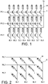
- 1T1R cells comprising three word lines WL1-WL3, eight bit lines BL1-BL8 each intended to be connected to an output neuron and a source line (or "Source-Line”) SL connected to all synapses.
- Source-Line source line
- 1S1R cells composed of a variable resistor M and a selector S having a behavior similar to a diode, or even to two diodes head to tail.
- Each 1S1R cell is a dipole whose terminals constitute the activation and propagation terminals, and the synaptic plane is organized as shown in picture 2 where we have taken the example of a plane comprising three word lines WL1-WL3 and four bit lines BL1-BL4, and where each synapse is taken between a voltage on the corresponding word line and a voltage on its corresponding bit line.
- this organization offers an “all-to-all” connection whereby all presynaptic neurons are connected via a synapse to all postsynaptic neurons.
- this “all-to-all” connection can lead to a mainly null synaptic matrix and therefore to low energy efficiency.
- This organization also necessitates having to fine-tune the zero weights under penalty of having a network composed mainly of parasitic synapses, making the analogical integration of the synaptic weights even more complex.
- RRAM memory which is composed of an insulator wedged between two layers of conductors. In a first stage of formation, a conductive wire grows from one of the conductors to the other, thus reducing the total resistance of the dipole. Once this wire is formed, the writing actions act on its length to vary the resistance. A Set operation lengthens the wire and reduces the resistance while a Reset operation has the opposite effect. Reading an OxRAM memory presents a difficulty, that of spurious writing by gradually modifying the value of the resistance over successive readings. To limit this risk, it is advisable to apply a maximum read voltage of 100 mV.
- V spike _ pre limits the membrane voltage V mem , because the membrane capacitance C mem is charged through the resistor R synb to which V spike _ pre is applied. In other words, the membrane voltage is at most the voltage V spike_pre .
- V mem being an analog calculation element therefore subject in particular to problems of noise, technological variations, capacitive coupling, its voltage range cannot be reduced to a value as low as 100 mV without greatly increasing the sources of errors Calculation.
- RRAM devices often have a low resistance range (with low values of the order of k ⁇ ) and that one can therefore be confronted with time constants of the cut R syn - C mem of l order of a nanosecond or even less.
- the read pulse must also be propagated over the entire width of the synaptic plane.
- the shorter this pulse the less “clean” it is in the end.
- the object of the invention is to provide a solution making it possible to respond to one and/or the other of the aforementioned constraints. It is set out in the attached set of claims.
- the invention relates to an artificial neuron NA for a neuromorphic chip comprising a synapse with resistive memory representative of a synaptic weight.
- the synapse has a synapse activation terminal and a synaptic signal propagation terminal.
- the propagation terminal propagates a synaptic signal representative of the value of the resistive memory (i.e. the synaptic weight) in the direction of the artificial neuron NA via a BL bit line.
- the artificial neuron comprises an integration circuit Cl which comprises a synaptic weight accumulator ACC at the terminals of which a membrane voltage V mem is established and a comparator COMP configured to emit a postsynaptic pulse SO in the event of crossing a threshold V threshold by the membrane voltage V mem .
- the invention proposes to decouple the reading of the synaptic weight from its integration by avoiding digitizing the reading of the synaptic weight.
- the different constraints can thus be distributed according to whether they are inherited from resistive memory technology or from the operation of the analog neuron.
- the invention proposes more particularly that the artificial neuron NA further comprises a reading circuit CL configured to impose on the synapse a reading voltage independent of the membrane voltage V mem and to supply the integration circuit Cl with an analog quantity representative of the synaptic weight PSa.
- the read circuit CL thus makes it possible to impose on the synapse a read voltage having an identical polarization for each read regardless of the state of the membrane voltage V mem .
- This read circuit also makes it possible to impose on the synapse a sufficiently low read voltage to avoid any risk of parasitic writing.
- the result of the reading namely the analog quantity representative of the synaptic weight PSa, is transmitted to the integration circuit.
- this quantity is a duration, while in other embodiments not falling within the scope of the invention, this quantity can take various other forms, such as a voltage, a current or a charge. for example.
- the integration circuit C1 thus decoupled from the reading, can thus offer a wide voltage range for the membrane voltage, independent of the specifications of the synapse.
- synapses which can be both excitatory and inhibitory, and which must therefore be capable of both injecting and drawing current from the neuron.
- the synapses here being resistive and the current that they control depending on their resistance, two supply voltage levels of the synapse are provided, one positive and one negative.
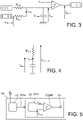
- the figure 6 provides an example of such an excitatory and inhibitory synapse, known as the 2R1C synapse.
- the synapse comprises an exciting component CE and an inhibiting component Cl arranged in series, with the midpoint of the propagation terminal Bp of the synapse, between a positive supply voltage V read and a negative supply voltage -V read .
- the synapse weight is encoded as follows. If one wants an excitatory synapse, the resistance R inhi is set to its maximum resistance level, while the resistance R exci ( ⁇ R inhi ) modulates the positive weight of the synapse. The lower the resistance R exci , the greater the synaptic weight, because it results in a higher synaptic current. Conversely, if we want an inhibitory synapse, the resistance R exci is set to its maximum resistance level, while the resistance R inhi ( ⁇ R exci ) modulates the negative weight of the synapse
- the diagram made up of the capacitor C load and two resistors R inhi and R exci is similar to a damped resistive bridge.
- the potential V load at the propagation terminal Bp is then gradually charged as represented on the figure 7 .
- This figure 7 illustrates that the integration of the synaptic weight can only be effective over an integration period PI corresponding to a read pulse duration less than the time constant of the couple R syn - C load .
- Rexci R inhi
- This time constant is also even shorter when binary RRAMs are used to obtain multivalued synapses, the paralleling of these binary RRAMs resulting in effect in a lower overall resistance.
- This problem can be circumvented by having recourse to a static reading of the synapse, that is to say to the reading of a quantity depending on the weight of the synapse which is stabilized in the sense that it is independent of the duration of a read pulse.
- the figure 7 indeed shows that in the static state reached with a sufficiently long read pulse, the value of V load can effectively be modulated by the ratio between R exci and R inhi and therefore by playing with the number of high resistance devices ( "High Resistive State”, HRS) or in low resistance (“Low Resistive State”, LRS) on the excitatory component side and the inhibitory component side.
- HRS High Resistive State
- LRS Low Resistive State
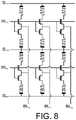
- the gates SL a , SLb are intended to remain biased at ⁇ V read and the write pulses between ground and V DD are sent to the activation terminals WL i , WL j . It is noted that the access transistors of the inhibiting cells are reverse biased.
- the excitatory component of a synapse is taken between a word line WL i_exci , WL j_exci and a bit line Bl u -Bl x while the inhibitory component of the same synapse is taken between a word line WL i_inhi , WL j_inhi and the bit line Bl u -Bl x .
- Read pulses are sent simultaneously on the word lines WL i_exci and WL i_inhi corresponding to a presynaptic spike afferent to line i.
- Word line WL i_exci is pulsed from ground to V read and word line WL i_inhi is pulsed from ground to -V read .
- these source lines SL a and SL b can change polarization (from V read to ⁇ V read and vice versa) only when necessary by exploiting a memory in each source line driver for this purpose.
- the figure 10 and 11 illustrate another exemplary embodiment for integrating an analog signed weight into a synaptic plane according to which an analog absolute value is associated with a binary sign by means of a synapse referred to below as absolute value+sign synapse.
- the synaptic plane is then more conventional, equipped with a single read voltage and presenting unidirectional read currents.
- a certain number of binary RRAMs, a multivalued RRAM or a single binary RRAM in case of binary synapse implement(s) the absolute value R abs of the synaptic weight while another RRAM, modeled by a resistance R sign , is used in a binary way to encode the sign of the synaptic weight.
- This sign RRAM can advantageously be constituted by a triplet or a quintuplet of devices from which the sign of the synapse is extracted by the majority.
- the reading circuit of the artificial neuron then comprises a binary reading circuit Cb of the sign memory of synaptic weight M sign and an analog reading circuit Ca of the memory of absolute value of synaptic weight M abs , said analog reading circuit Ca being driven by the binary read circuit Cb.
- the binary reading circuit Cb exploits the sign of the presynaptic spike Sp and the sign of the synaptic weight M sign to provide the analog reading circuit Ca with an integration sign Si indicating in which direction to integrate the analog current I abs coming from the memory of absolute value of synaptic weight M abs .
- the analog quantity representative of the synaptic weight supplied by the read circuit to the integration circuit is a voltage.
- the analog quantity representative of the synaptic weight can be a voltage independent of the duration of a reading pulse, the neurons carrying out a static reading of the synapse.
- the read circuit CL1 comprises a synaptic current accumulator C load at the terminals of which a voltage V load is established, this voltage corresponding to the analog quantity representative of the synaptic weight.
- the artificial neuron also comprises a bidirectional voltage follower circuit ST1, ST2 interposed between the read circuit CL1 and the integration circuit CI1.
- the functioning of the neuron is as follows.
- the lower pole of C load is connected to the virtual ground Gnd by a switch rst_bot.
- C load is first discharged by connecting its upper pole to virtual ground using an rst_top switch, the read circuit thus being configured to discharge the accumulator from synaptic current C load before imposing the read voltage on the synapse.
- the reading of the synapse is then triggered by the opening of the rst_top switch.
- the current coming from the bit line BL is then accumulated in C load , generating the read voltage V load . Opening rst_bot makes it possible to obtain a floating voltage V load .
- the voltage follower ST1, ST2 is then configured to copy the membrane voltage V mem to the lower terminal of C load .
- the voltage at the upper terminal of C load is equal to the addition of V mem and V load .
- the voltage follower ST1, ST2 is configured to copy this voltage addition to the upper terminal of the membrane capacitance C mem thus providing the new membrane voltage which is compared to the spike emission threshold(s) (s).
- the analog voltage addition proposed in the example embodiments of figures 11 and 12 allows a static reading of the 2R1C synapse. Dynamic reading is also possible provided that a sufficiently short reading pulse is generated.
- the maximum stimulation is limited by the read voltage of the RRAMs. It is then possible to choose that such a maximum stimulation alone makes it possible to trigger a postsynaptic spike by a neuron whose membrane tension would be at its resting potential. In which case, the voltage range of the membrane voltage V mem is limited by the read voltage V read . Alternatively, such a stimulation characteristic is not provided, and the membrane voltage V mem can be spread over a wider voltage range.
- the voltage follower ST1 comprises two operational amplifiers, one intended via the mem2bot switch to copy the membrane voltage to the lower terminal of C load and the other intended via the top2mem switch to copy the voltage addition at the upper bound of C mem .
- the voltage follower ST2 comprises a single operational amplifier instead of the two operational amplifiers used alternately on the figure 12 .
- an additional capacitor C load_bis is provided in parallel with the switch rst_bot.
- the synapse absolute value + sign is adapted to the neurons of the figure 12 and 13 .
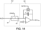
- the reading circuit CL2 comprises a switch R ON /R OFF having a first terminal B1 intended to be connected to the synapse via the bit line BL and a second terminal B2 connected to the integration circuit Cl2.
- the integration circuit C12 comprises an integrator circuit connected to the second terminal and within which the synaptic weight accumulator C mem is mounted.
- Reading the synapse is done as follows. Initially, the switch is left open (it has a resistance R OFF in its blocked state), the voltage on the bit line V BL stabilizes according to the weight of the synapse (there must therefore be R OFF >>HRS ). In a second time, the switch is closed (it presents a resistance R ON in its on state), the voltage V BL is integrated by the integrator assembly whose time constant depends on R ON and C mem and not on the LRS of the RRAMs. We therefore have R ON >LRS. The neuron of figure 14 thus performs a static reading of the synapse by means of the switch R ON /R OFF and an integration of the voltage V BL .
- the neuron comprises a logic circuit LOG interposed between the read circuit CL3 and the integration circuit CI3, the logic circuit being configured to generate from said analog quantity a pulse Cmd_exci, Cmd_inhi having said duration.
- the integration circuit Cl3 for its part comprises a current source SI exc , SI inhi driven by said pulse to inject a current into the synaptic weight accumulator for said duration.
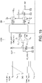
- the reading circuit CL3 of the neuron represented in figure 15 comprises a synaptic current accumulator C load at the terminals of which a voltage V load is established and a switch rst_load making it possible to carry out the discharge of this accumulator before an operation of reading the synaptic weight.
- the accumulator C load is charged by the synaptic current, more or less rapidly depending on the synaptic weight. The duration of this charging can be estimated very simply using an analog comparator.
- the Comp_exci output of the comparator Cp is supplied to the logic circuit LOG interposed between the read circuit CL3 and the integration circuit Cl3.
- This logic circuit is configured to generate, from the result of the comparison, a voltage pulse having said duration, in this case the Cmd_exci pulse in the example of figure 15 .
- the integration circuit Cl2 for its part comprises a current source SI exc controlled by said pulse Cmd_exci to inject a current into the synaptic weight accumulator C mem during said duration.
- the duration of this current injection therefore depends on the value of the synaptic weight, so that the final value of the membrane voltage V mem also depends on the value of the synaptic weight.
- the integration circuit Cl2 comprises another current source SI inhi driven by a voltage pulse Cmd_inhi to draw current from the accumulator of synaptic weights C mem for a duration representative of the synaptic weight.
- the neuron of figure 15 can also take into account the sign of the presynaptic pulse, the latter Sign_spike being supplied to the logic circuit LOG which is then configured to determine the sign of integration from the sign of the spike and weight sign information synaptic synapse determined by which of the comparators Cp and Cn switches.
- This logical and economical processing of the spike sign makes it possible, particularly in the case of 1T1R cells, to lighten the synaptic plane and its management. Note that the absolute value + sign synapse is particularly suited to this neuron.
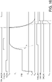
- the pulse is generated from two comparator switchings, its duration corresponding to a duration separating the crossing of the threshold associated with one of the comparators then the crossing of the threshold associated with the other of the comparators .
- the switching delays are thus applied to the start and end of the pulse and therefore do not affect its duration.
- the synapse is read in one direction long enough for V load to go into abutment on V read or -V read depending on the sign of the synapse. Then, the reading polarization is reversed, the voltage V load will therefore cross the potential difference from one polarization of V read to the other and cross the two thresholds Sp, Sn in a time relative to the weight of the synapse.
- the logic circuit LOG is then configured to generate a voltage pulse between these two comparator switchings.
- the read circuit CL4, CL5 comprises a current conveyor which comprises an input port X intended to be connected to the synapse via the bit line, an input port Y intended to have a fixed voltage imposed on it (by mass) for the duration of the access to the synapse and an output port Z connected to the integration circuit.
- Such a current conveyor based on an operational amplifier and two current mirrors, is such that the fixed voltage imposed on input port Y is copied to input port X and the current injected into the input port X is reproduced on the output port Z (with a sign inversion for the circuit of the figure 17 , without sign inversion for the circuit of the figure 18 ).
- a fixed voltage being imposed on port Y the bit line voltage is slaved to this fixed voltage (it is thus independent of the membrane voltage of the neuron) and the synaptic current is delivered to the output port Z. This synaptic current is supplied to the integration circuit which will then carry out an analog integration thereof.
- the current conveyor comprises, as shown in figure 19 , a current mirror configured to lower the current between the input port X and the output port Z.
- I OUT ⁇ I IN K , with K a factor greater than 1 which makes it possible to use read pulses of longer duration and therefore more suited to the operation of the active elements without thereby saturating the membrane capacitance.
- the neuron comprises a transmission gate T between the read circuit and the integration circuit.
- This gate makes it possible to dissociate the access time to the RRAMs and the integration time, which makes it possible to wait for the voltage on the input port X to stabilize before integrating the read current and playing with a short integration pulse without requiring a particularly reactive operational amplifier.
- the read circuit CL6 advantageously comprises both the inverting current mirror of the read circuit CL4 and the non-inverting current mirror of the read circuit CL5 (these mirrors being able to lower the current in accordance with the figure 19 ) and a selector S controlled by a Sign_spike signal representative of the sign of the presynaptic spike to select the output of one or the other of these current mirrors.
- the invention is not limited to the artificial neuron previously described, but extends to a neuromorphic chip comprising a plurality of resistive memory synapses arranged in a network with transverse rows and columns. Each synapse has a propagation terminal, the propagation terminals of the synapses of the same column being interconnected and connected to an artificial neuron according to the invention.
- the synapses can be excitatory or inhibitory synapses such as those presented previously in connection with the figures 6 to 11 .
Landscapes
- Engineering & Computer Science (AREA)
- Physics & Mathematics (AREA)
- Health & Medical Sciences (AREA)
- Life Sciences & Earth Sciences (AREA)
- Biomedical Technology (AREA)
- Theoretical Computer Science (AREA)
- Biophysics (AREA)
- General Health & Medical Sciences (AREA)
- Molecular Biology (AREA)
- Neurology (AREA)
- General Physics & Mathematics (AREA)
- Computational Linguistics (AREA)
- Computing Systems (AREA)
- General Engineering & Computer Science (AREA)
- Data Mining & Analysis (AREA)
- Mathematical Physics (AREA)
- Software Systems (AREA)
- Artificial Intelligence (AREA)
- Evolutionary Computation (AREA)
- Computer Hardware Design (AREA)
- Semiconductor Memories (AREA)
- Heterocyclic Carbon Compounds Containing A Hetero Ring Having Oxygen Or Sulfur (AREA)
Claims (7)
- Künstliches Neuron (NA) für einen neuromorphen Chip, enthaltend eine Synapse mit resistivem Speicher, der für ein Synapsengewicht repräsentativ ist,wobei das künstliche Neuron eine Integrationsschaltung (CI3) umfasst, die einen Synapsengewichtsakkumulator (Cmem), an dessen Anschlüssen sich eine Membranspannung (Vmem) einstellt, und einen Komparator (COMP) umfasst, der dazu ausgelegt ist, einen postsynaptischen Impuls auszusenden, wenn die Membranspannung einen Schwellenwert überschreitet,wobei das künstliche Neuron dadurch gekennzeichnet ist, dass es ferner umfasst:eine Leseschaltung (CL3), die einen Synapsenstromakkumulator (Cload) umfasst, wobei die Leseschaltung (CL3) dazu ausgelegt ist, der Synapse eine von der Membranspannung unabhängige Lesespannung aufzuprägen, eine Ladezeitdauerinformation des Synapsenstromakkumulators (Cload) zu bestimmen und eine für das Synapsengewicht repräsentative analoge Größe (PSa) bereitzustellen, wobei die analoge Größe die Ladezeitdauerinformation ist;eine Logikschaltung (LOG), die zwischen Leseschaltung (CL3) und Integrationsschaltung (CI3) geschaltet ist, wobei die Logikschaltung dazu ausgelegt ist, aus der analogen Größe einen Impuls (Cmd_exci, Cmd_inhi) zu erzeugen, der als Zeitdauer die Ladezeitdauer des Synapsenstromakkumulators (Cload) hat; unddass die Integrationsschaltung (CI3) eine Stromquelle (SIexc, SIinhi) umfasst, die von dem Impuls angesteuert wird, um während der Zeitdauer des Impulses einen Strom in den Synapsengewichtsakkumulator einzukoppeln.
- Künstliches Neuron nach Anspruch 1, wobei die Leseschaltung (CL3) zumindest einen Komparator (Cp, Cn) für die Spannung an den Anschlüssen des Synapsenstromakkumulators mit einem Schwellenwert (Sp, Sn) umfasst, um ein Vergleichsergebnis zu liefern, das die analoge Größe darstellt.
- Künstliches Neuron nach Anspruch 2, wobei der zumindest eine Komparator (Cp, Cn) der Leseschaltung (CL3) einen ersten Komparator (CP) mit einem ersten Schwellenwert (Sp) und einen zweiten Komparator (Cn) mit einem zweiten Schwellenwert (Sn) umfasst und wobei die Logikschaltung dazu ausgelegt ist, ein Integrationsvorzeichen zu bestimmen, indem sie ein Signal (Signe_spike), das für ein präsynaptisches Impulsvorzeichen repräsentativ ist, und eine Synapsengewichtsvorzeicheninformation auswertet, die von demjenigen aus erstem und zweitem Komparator (Cp, Cn) bestimmt wird, der schaltet.
- Künstliches Neuron nach Anspruch 2, wobei der zumindest eine Komparator (Cp, Cn) der Leseschaltung (CL3) einen ersten Komparator (Cp) mit einem ersten Schwellenwert (Sp) und einen zweiten Komparator (Cn) mit einem zweiten Schwellenwert (Sn) umfasst und wobei die Logikschaltung so ausgelegt ist, dass die Zeitdauer des Impulses einer Zeitdauer entspricht, die zwischen dem Überschreiten eines der Schwellenwerte (Sp, Sn) und dem Überschreiten des anderen der Schwellenwerte (Sp, Sn) liegt.
- Künstliches Neuron nach einem der Ansprüche 1 bis 4, wobei bei der Synapse mit einem Speicher für den absoluten Wert des Synapsengewichts (Mabs) und mit einem Speicher für das Synapsengewichtvorzeichen (Msigne) die Leseschaltung eine binäre Leseschaltung (Cb) für den Speicher für das Synapsengewichtvorzeichen und eine analoge Leseschaltung (Ca) für den Speicher für den absoluten Wert des Synapsengewichts Mabs umfasst, die von der binären Leseschaltung angesteuert wird.
- Neuromorpher Chip mit einer Vielzahl von Synapsen mit resistivem Speicher, die in einem Netzwerk mit Zeilen und quer verlaufenden Spalten angeordnet sind, wobei jede Synapse über einen Anschluss zur Ausbreitung eines synaptischen Signals verfügt, wobei die Synapsenausbreitungsanschlüsse in derselben Spalte miteinander verbunden und an ein künstliches Neuron nach einem der Ansprüche 1 bis 5 angeschlossen sind.
- Neuromorpher Chip nach Anspruch 6, wobei jede Synapse eine erregende Komponente und eine hemmende Komponente umfasst, die durch den Synapsenausbreitungsanschluss in Reihe geschaltet sind.
Applications Claiming Priority (1)
| Application Number | Priority Date | Filing Date | Title |
|---|---|---|---|
| FR1872515A FR3089663B1 (fr) | 2018-12-07 | 2018-12-07 | Neurone artificiel pour puce neuromorphique à synapses résistives |
Publications (2)
| Publication Number | Publication Date |
|---|---|
| EP3663988A1 EP3663988A1 (de) | 2020-06-10 |
| EP3663988B1 true EP3663988B1 (de) | 2022-05-18 |
Family
ID=66049326
Family Applications (1)
| Application Number | Title | Priority Date | Filing Date |
|---|---|---|---|
| EP19212046.7A Not-in-force EP3663988B1 (de) | 2018-12-07 | 2019-11-28 | Künstliches neuron für neuromorphen chip mit resistiven synapsen |
Country Status (3)
| Country | Link |
|---|---|
| US (1) | US11630993B2 (de) |
| EP (1) | EP3663988B1 (de) |
| FR (1) | FR3089663B1 (de) |
Families Citing this family (23)
| Publication number | Priority date | Publication date | Assignee | Title |
|---|---|---|---|---|
| US11188815B2 (en) | 2019-01-07 | 2021-11-30 | International Business Machines Corporation | Weight shifting for neuromorphic synapse array |
| KR102810722B1 (ko) * | 2019-11-08 | 2025-05-22 | 삼성전자주식회사 | 시냅스 소자 및 시냅스 소자를 포함하는 뉴로모픽 프로세서 |
| US20210406661A1 (en) | 2020-06-25 | 2021-12-30 | PolyN Technology Limited | Analog Hardware Realization of Neural Networks |
| EP3963514A1 (de) * | 2020-06-25 | 2022-03-09 | PolyN Technology Limited | Analoge hardware-realisierung neuronaler netze |
| US12347421B2 (en) | 2020-06-25 | 2025-07-01 | PolyN Technology Limited | Sound signal processing using a neuromorphic analog signal processor |
| US11885271B2 (en) | 2020-06-25 | 2024-01-30 | PolyN Technology Limited | Systems and methods for detonation control in spark ignition engines using analog neuromorphic computing hardware |
| KR102507770B1 (ko) * | 2020-08-26 | 2023-03-07 | 국민대학교산학협력단 | 시냅스 및 시냅스 어레이와, 이를 이용한 컴퓨팅 시스템 및 그 구동 방법 |
| TW202546696A (zh) * | 2020-10-30 | 2025-12-01 | 荷蘭商因納特拉納米系統有限公司 | 用於分佈式多組件突觸計算結構之尖峰神經網路及方法 |
| WO2022118340A1 (en) * | 2020-12-03 | 2022-06-09 | Indian Institute Of Technology Delhi | Novel activation function with hardware realization for recurrent neuromorphic networks |
| US11741353B2 (en) | 2020-12-09 | 2023-08-29 | International Business Machines Corporation | Bias scheme for single-device synaptic element |
| KR102782347B1 (ko) | 2021-06-08 | 2025-03-18 | 한국전자통신연구원 | 스파이크 뉴럴 네트워크 회로 |
| CN113408613B (zh) * | 2021-06-18 | 2022-07-19 | 电子科技大学 | 一种基于延迟机制的单层图像分类方法 |
| CN113673674B (zh) * | 2021-08-09 | 2025-03-14 | 江南大学 | 一种基于cmos的模拟脉冲神经元电路 |
| CN113643741B (zh) * | 2021-08-16 | 2023-12-15 | 湖北大学 | 一种基于1s1r的逻辑运算单元及运算方法 |
| KR102579571B1 (ko) | 2021-12-03 | 2023-09-15 | 아주대학교산학협력단 | 스파이킹 신경망 구조의 픽셀화된 모놀리식 광혈류측정 센서 및 그의 구동 방법 |
| EP4457701A4 (de) * | 2021-12-30 | 2025-12-31 | Polyn Tech Limited | Transformationen, optimierungen und schnittstellen zur analogen hardware-realisierung neuronaler netze |
| US20230351165A1 (en) * | 2022-05-02 | 2023-11-02 | Taiwan Semiconductor Manufacturing Company, Ltd. | Method for operating neural network |
| JP7788683B2 (ja) * | 2022-05-21 | 2025-12-19 | 浩志 渡辺 | シリコンブレイン |
| KR102689274B1 (ko) * | 2022-07-21 | 2024-07-29 | 경북대학교 산학협력단 | 멤리스터를 이용한 펄스 발생 방법, 이를 수행하기 위한 기록 매체 및 장치 |
| CN115392442B (zh) * | 2022-10-26 | 2023-01-24 | 深圳时识科技有限公司 | 神经元点火方法、芯片及电子设备 |
| US11823037B1 (en) | 2023-02-28 | 2023-11-21 | PolyN Technology Limited | Optocoupler-based flexible weights in neuromorphic analog signal processors |
| CN116523010B (zh) * | 2023-05-10 | 2025-12-19 | 湘潭大学 | 一种lif神经元电路 |
| CN118428428B (zh) * | 2024-05-16 | 2024-09-27 | 湖南师范大学 | 一种基于忆阻器阈值特性的神经元自学习电路 |
Family Cites Families (5)
| Publication number | Priority date | Publication date | Assignee | Title |
|---|---|---|---|---|
| US20120011092A1 (en) * | 2010-07-07 | 2012-01-12 | Qualcomm Incorporated | Methods and systems for memristor-based neuron circuits |
| US10671911B2 (en) * | 2016-02-19 | 2020-06-02 | International Business Machines Corporation | Current mirror scheme for an integrating neuron circuit |
| US10922608B2 (en) * | 2017-03-08 | 2021-02-16 | Arm Ltd | Spiking neural network |
| US12106211B2 (en) * | 2017-04-27 | 2024-10-01 | The Regents Of The University Of California | Mixed signal neuromorphic computing with nonvolatile memory devices |
| US11501141B2 (en) * | 2018-10-12 | 2022-11-15 | Western Digital Technologies, Inc. | Shifting architecture for data reuse in a neural network |
-
2018
- 2018-12-07 FR FR1872515A patent/FR3089663B1/fr not_active Expired - Fee Related
-
2019
- 2019-11-28 EP EP19212046.7A patent/EP3663988B1/de not_active Not-in-force
- 2019-12-04 US US16/703,465 patent/US11630993B2/en active Active
Also Published As
| Publication number | Publication date |
|---|---|
| US20200202206A1 (en) | 2020-06-25 |
| FR3089663B1 (fr) | 2021-09-17 |
| EP3663988A1 (de) | 2020-06-10 |
| FR3089663A1 (fr) | 2020-06-12 |
| US11630993B2 (en) | 2023-04-18 |
Similar Documents
| Publication | Publication Date | Title |
|---|---|---|
| EP3663988B1 (de) | Künstliches neuron für neuromorphen chip mit resistiven synapsen | |
| EP3660749A1 (de) | Neuronaler schaltkreis, der in der lage ist, einen synaptischen lernprozess auszuführen | |
| EP2713318B1 (de) | Neuromorphes System, das die intrinsischen Eigenschaften von Speicherzellen nutzt | |
| WO2014135801A1 (fr) | Organe à neurone artificiel et memristor | |
| WO2013000940A1 (fr) | Reseau de neurones artificiels a base de dispositifs memristifs complementaires | |
| WO2013000939A1 (fr) | Méthode d'apprentissage non supervisée dans un réseau de neurones artificiel a base de nano-dispositifs memristifs et réseau de neurones artificiel mettant en oeuvre la méthode | |
| EP2833364A2 (de) | Nichtflüchtige magnetische Speichervorrichtung mit drei Elektroden und entsprechende Matrix | |
| EP4137999B1 (de) | Neuromorpher schaltkreis auf der basis von 2t2r-rram-zellen | |
| EP4292017A1 (de) | Neuromorphe schaltung und zugehöriges trainingsverfahren | |
| FR3106681A1 (fr) | Architecture neuromorphique | |
| EP4224477B1 (de) | Dreidimensionale speicherstruktur zur speicherberechnung | |
| EP4020479A1 (de) | Differentielles lesen eines rram-speichers mit geringem stromverbrauch | |
| EP4195207B1 (de) | Nichtflüchtige speicher in oxram/feram-mischtechnologie | |
| EP4576094A1 (de) | Elektronische schaltung auf rram 2t2r-zellenbasis mit verbesserter genauigkeit | |
| WO2018100325A1 (fr) | Dispositif et procède de modulation, synapse artificielle comportant ledit dispositif de modulation, procède de plasticité a court terme dans un réseau de neurones artificiels comportant ladite synapse artificielle | |
| EP4276833A1 (de) | Speicherzelle, elektronische schaltung mit solchen zellen, programmierverfahren und multiplizier- und akkumulationsverfahren dafür | |
| EP4120271A1 (de) | Leseverfahren eines mehrstufigen rram-speichers | |
| EP4354351B1 (de) | Elektronische schaltung auf rram-zellenbasis | |
| FR2756409A1 (fr) | Circuit de lecture pour memoire | |
| EP4283621A1 (de) | Verfahren zur berechnung eines mac-betriebs in einem 1s1r-ram-speicher | |
| WO2025228731A1 (fr) | Lecture différentielle multi-valuée d'un dispositif mémoire | |
| EP4345821A1 (de) | In eine datenspeicherschaltung integrierte logische datenverarbeitungsschaltung | |
| FR3035998A1 (fr) | Non-volatile memory with programming circuit |
Legal Events
| Date | Code | Title | Description |
|---|---|---|---|
| PUAI | Public reference made under article 153(3) epc to a published international application that has entered the european phase |
Free format text: ORIGINAL CODE: 0009012 |
|
| STAA | Information on the status of an ep patent application or granted ep patent |
Free format text: STATUS: REQUEST FOR EXAMINATION WAS MADE |
|
| 17P | Request for examination filed |
Effective date: 20191128 |
|
| AK | Designated contracting states |
Kind code of ref document: A1 Designated state(s): AL AT BE BG CH CY CZ DE DK EE ES FI FR GB GR HR HU IE IS IT LI LT LU LV MC MK MT NL NO PL PT RO RS SE SI SK SM TR |
|
| AX | Request for extension of the european patent |
Extension state: BA ME |
|
| GRAP | Despatch of communication of intention to grant a patent |
Free format text: ORIGINAL CODE: EPIDOSNIGR1 |
|
| STAA | Information on the status of an ep patent application or granted ep patent |
Free format text: STATUS: GRANT OF PATENT IS INTENDED |
|
| INTG | Intention to grant announced |
Effective date: 20211221 |
|
| GRAS | Grant fee paid |
Free format text: ORIGINAL CODE: EPIDOSNIGR3 |
|
| GRAA | (expected) grant |
Free format text: ORIGINAL CODE: 0009210 |
|
| STAA | Information on the status of an ep patent application or granted ep patent |
Free format text: STATUS: THE PATENT HAS BEEN GRANTED |
|
| AK | Designated contracting states |
Kind code of ref document: B1 Designated state(s): AL AT BE BG CH CY CZ DE DK EE ES FI FR GB GR HR HU IE IS IT LI LT LU LV MC MK MT NL NO PL PT RO RS SE SI SK SM TR |
|
| REG | Reference to a national code |
Ref country code: GB Ref legal event code: FG4D Free format text: NOT ENGLISH |
|
| REG | Reference to a national code |
Ref country code: CH Ref legal event code: EP |
|
| REG | Reference to a national code |
Ref country code: IE Ref legal event code: FG4D Free format text: LANGUAGE OF EP DOCUMENT: FRENCH |
|
| REG | Reference to a national code |
Ref country code: DE Ref legal event code: R096 Ref document number: 602019015069 Country of ref document: DE |
|
| REG | Reference to a national code |
Ref country code: AT Ref legal event code: REF Ref document number: 1493586 Country of ref document: AT Kind code of ref document: T Effective date: 20220615 |
|
| REG | Reference to a national code |
Ref country code: LT Ref legal event code: MG9D |
|
| REG | Reference to a national code |
Ref country code: NL Ref legal event code: MP Effective date: 20220518 |
|
| REG | Reference to a national code |
Ref country code: AT Ref legal event code: MK05 Ref document number: 1493586 Country of ref document: AT Kind code of ref document: T Effective date: 20220518 |
|
| PG25 | Lapsed in a contracting state [announced via postgrant information from national office to epo] |
Ref country code: SE Free format text: LAPSE BECAUSE OF FAILURE TO SUBMIT A TRANSLATION OF THE DESCRIPTION OR TO PAY THE FEE WITHIN THE PRESCRIBED TIME-LIMIT Effective date: 20220518 Ref country code: PT Free format text: LAPSE BECAUSE OF FAILURE TO SUBMIT A TRANSLATION OF THE DESCRIPTION OR TO PAY THE FEE WITHIN THE PRESCRIBED TIME-LIMIT Effective date: 20220919 Ref country code: NO Free format text: LAPSE BECAUSE OF FAILURE TO SUBMIT A TRANSLATION OF THE DESCRIPTION OR TO PAY THE FEE WITHIN THE PRESCRIBED TIME-LIMIT Effective date: 20220818 Ref country code: NL Free format text: LAPSE BECAUSE OF FAILURE TO SUBMIT A TRANSLATION OF THE DESCRIPTION OR TO PAY THE FEE WITHIN THE PRESCRIBED TIME-LIMIT Effective date: 20220518 Ref country code: LT Free format text: LAPSE BECAUSE OF FAILURE TO SUBMIT A TRANSLATION OF THE DESCRIPTION OR TO PAY THE FEE WITHIN THE PRESCRIBED TIME-LIMIT Effective date: 20220518 Ref country code: HR Free format text: LAPSE BECAUSE OF FAILURE TO SUBMIT A TRANSLATION OF THE DESCRIPTION OR TO PAY THE FEE WITHIN THE PRESCRIBED TIME-LIMIT Effective date: 20220518 Ref country code: GR Free format text: LAPSE BECAUSE OF FAILURE TO SUBMIT A TRANSLATION OF THE DESCRIPTION OR TO PAY THE FEE WITHIN THE PRESCRIBED TIME-LIMIT Effective date: 20220819 Ref country code: FI Free format text: LAPSE BECAUSE OF FAILURE TO SUBMIT A TRANSLATION OF THE DESCRIPTION OR TO PAY THE FEE WITHIN THE PRESCRIBED TIME-LIMIT Effective date: 20220518 Ref country code: ES Free format text: LAPSE BECAUSE OF FAILURE TO SUBMIT A TRANSLATION OF THE DESCRIPTION OR TO PAY THE FEE WITHIN THE PRESCRIBED TIME-LIMIT Effective date: 20220518 Ref country code: BG Free format text: LAPSE BECAUSE OF FAILURE TO SUBMIT A TRANSLATION OF THE DESCRIPTION OR TO PAY THE FEE WITHIN THE PRESCRIBED TIME-LIMIT Effective date: 20220818 Ref country code: AT Free format text: LAPSE BECAUSE OF FAILURE TO SUBMIT A TRANSLATION OF THE DESCRIPTION OR TO PAY THE FEE WITHIN THE PRESCRIBED TIME-LIMIT Effective date: 20220518 |
|
| PG25 | Lapsed in a contracting state [announced via postgrant information from national office to epo] |
Ref country code: RS Free format text: LAPSE BECAUSE OF FAILURE TO SUBMIT A TRANSLATION OF THE DESCRIPTION OR TO PAY THE FEE WITHIN THE PRESCRIBED TIME-LIMIT Effective date: 20220518 Ref country code: PL Free format text: LAPSE BECAUSE OF FAILURE TO SUBMIT A TRANSLATION OF THE DESCRIPTION OR TO PAY THE FEE WITHIN THE PRESCRIBED TIME-LIMIT Effective date: 20220518 Ref country code: LV Free format text: LAPSE BECAUSE OF FAILURE TO SUBMIT A TRANSLATION OF THE DESCRIPTION OR TO PAY THE FEE WITHIN THE PRESCRIBED TIME-LIMIT Effective date: 20220518 Ref country code: IS Free format text: LAPSE BECAUSE OF FAILURE TO SUBMIT A TRANSLATION OF THE DESCRIPTION OR TO PAY THE FEE WITHIN THE PRESCRIBED TIME-LIMIT Effective date: 20220918 |
|
| PG25 | Lapsed in a contracting state [announced via postgrant information from national office to epo] |
Ref country code: SM Free format text: LAPSE BECAUSE OF FAILURE TO SUBMIT A TRANSLATION OF THE DESCRIPTION OR TO PAY THE FEE WITHIN THE PRESCRIBED TIME-LIMIT Effective date: 20220518 Ref country code: SK Free format text: LAPSE BECAUSE OF FAILURE TO SUBMIT A TRANSLATION OF THE DESCRIPTION OR TO PAY THE FEE WITHIN THE PRESCRIBED TIME-LIMIT Effective date: 20220518 Ref country code: RO Free format text: LAPSE BECAUSE OF FAILURE TO SUBMIT A TRANSLATION OF THE DESCRIPTION OR TO PAY THE FEE WITHIN THE PRESCRIBED TIME-LIMIT Effective date: 20220518 Ref country code: EE Free format text: LAPSE BECAUSE OF FAILURE TO SUBMIT A TRANSLATION OF THE DESCRIPTION OR TO PAY THE FEE WITHIN THE PRESCRIBED TIME-LIMIT Effective date: 20220518 Ref country code: DK Free format text: LAPSE BECAUSE OF FAILURE TO SUBMIT A TRANSLATION OF THE DESCRIPTION OR TO PAY THE FEE WITHIN THE PRESCRIBED TIME-LIMIT Effective date: 20220518 Ref country code: CZ Free format text: LAPSE BECAUSE OF FAILURE TO SUBMIT A TRANSLATION OF THE DESCRIPTION OR TO PAY THE FEE WITHIN THE PRESCRIBED TIME-LIMIT Effective date: 20220518 |
|
| REG | Reference to a national code |
Ref country code: DE Ref legal event code: R097 Ref document number: 602019015069 Country of ref document: DE |
|
| PLBE | No opposition filed within time limit |
Free format text: ORIGINAL CODE: 0009261 |
|
| STAA | Information on the status of an ep patent application or granted ep patent |
Free format text: STATUS: NO OPPOSITION FILED WITHIN TIME LIMIT |
|
| PG25 | Lapsed in a contracting state [announced via postgrant information from national office to epo] |
Ref country code: AL Free format text: LAPSE BECAUSE OF FAILURE TO SUBMIT A TRANSLATION OF THE DESCRIPTION OR TO PAY THE FEE WITHIN THE PRESCRIBED TIME-LIMIT Effective date: 20220518 |
|
| 26N | No opposition filed |
Effective date: 20230221 |
|
| PG25 | Lapsed in a contracting state [announced via postgrant information from national office to epo] |
Ref country code: SI Free format text: LAPSE BECAUSE OF FAILURE TO SUBMIT A TRANSLATION OF THE DESCRIPTION OR TO PAY THE FEE WITHIN THE PRESCRIBED TIME-LIMIT Effective date: 20220518 |
|
| PG25 | Lapsed in a contracting state [announced via postgrant information from national office to epo] |
Ref country code: MC Free format text: LAPSE BECAUSE OF FAILURE TO SUBMIT A TRANSLATION OF THE DESCRIPTION OR TO PAY THE FEE WITHIN THE PRESCRIBED TIME-LIMIT Effective date: 20220518 |
|
| REG | Reference to a national code |
Ref country code: CH Ref legal event code: PL |
|
| REG | Reference to a national code |
Ref country code: BE Ref legal event code: MM Effective date: 20221130 |
|
| PG25 | Lapsed in a contracting state [announced via postgrant information from national office to epo] |
Ref country code: LI Free format text: LAPSE BECAUSE OF NON-PAYMENT OF DUE FEES Effective date: 20221130 Ref country code: CH Free format text: LAPSE BECAUSE OF NON-PAYMENT OF DUE FEES Effective date: 20221130 |
|
| PG25 | Lapsed in a contracting state [announced via postgrant information from national office to epo] |
Ref country code: LU Free format text: LAPSE BECAUSE OF NON-PAYMENT OF DUE FEES Effective date: 20221128 |
|
| PG25 | Lapsed in a contracting state [announced via postgrant information from national office to epo] |
Ref country code: IE Free format text: LAPSE BECAUSE OF NON-PAYMENT OF DUE FEES Effective date: 20221128 |
|
| PG25 | Lapsed in a contracting state [announced via postgrant information from national office to epo] |
Ref country code: BE Free format text: LAPSE BECAUSE OF NON-PAYMENT OF DUE FEES Effective date: 20221130 |
|
| PG25 | Lapsed in a contracting state [announced via postgrant information from national office to epo] |
Ref country code: IT Free format text: LAPSE BECAUSE OF FAILURE TO SUBMIT A TRANSLATION OF THE DESCRIPTION OR TO PAY THE FEE WITHIN THE PRESCRIBED TIME-LIMIT Effective date: 20220518 |
|
| PGFP | Annual fee paid to national office [announced via postgrant information from national office to epo] |
Ref country code: FR Payment date: 20231121 Year of fee payment: 5 Ref country code: DE Payment date: 20231120 Year of fee payment: 5 |
|
| PG25 | Lapsed in a contracting state [announced via postgrant information from national office to epo] |
Ref country code: HU Free format text: LAPSE BECAUSE OF FAILURE TO SUBMIT A TRANSLATION OF THE DESCRIPTION OR TO PAY THE FEE WITHIN THE PRESCRIBED TIME-LIMIT; INVALID AB INITIO Effective date: 20191128 |
|
| PG25 | Lapsed in a contracting state [announced via postgrant information from national office to epo] |
Ref country code: CY Free format text: LAPSE BECAUSE OF FAILURE TO SUBMIT A TRANSLATION OF THE DESCRIPTION OR TO PAY THE FEE WITHIN THE PRESCRIBED TIME-LIMIT Effective date: 20220511 |
|
| PG25 | Lapsed in a contracting state [announced via postgrant information from national office to epo] |
Ref country code: MK Free format text: LAPSE BECAUSE OF FAILURE TO SUBMIT A TRANSLATION OF THE DESCRIPTION OR TO PAY THE FEE WITHIN THE PRESCRIBED TIME-LIMIT Effective date: 20220511 |
|
| GBPC | Gb: european patent ceased through non-payment of renewal fee |
Effective date: 20231128 |
|
| PG25 | Lapsed in a contracting state [announced via postgrant information from national office to epo] |
Ref country code: MT Free format text: LAPSE BECAUSE OF FAILURE TO SUBMIT A TRANSLATION OF THE DESCRIPTION OR TO PAY THE FEE WITHIN THE PRESCRIBED TIME-LIMIT Effective date: 20220511 |
|
| PG25 | Lapsed in a contracting state [announced via postgrant information from national office to epo] |
Ref country code: GB Free format text: LAPSE BECAUSE OF NON-PAYMENT OF DUE FEES Effective date: 20231128 |
|
| PG25 | Lapsed in a contracting state [announced via postgrant information from national office to epo] |
Ref country code: GB Free format text: LAPSE BECAUSE OF NON-PAYMENT OF DUE FEES Effective date: 20231128 |
|
| PG25 | Lapsed in a contracting state [announced via postgrant information from national office to epo] |
Ref country code: BG Free format text: LAPSE BECAUSE OF FAILURE TO SUBMIT A TRANSLATION OF THE DESCRIPTION OR TO PAY THE FEE WITHIN THE PRESCRIBED TIME-LIMIT Effective date: 20220518 |
|
| PG25 | Lapsed in a contracting state [announced via postgrant information from national office to epo] |
Ref country code: BG Free format text: LAPSE BECAUSE OF FAILURE TO SUBMIT A TRANSLATION OF THE DESCRIPTION OR TO PAY THE FEE WITHIN THE PRESCRIBED TIME-LIMIT Effective date: 20220518 |
|
| REG | Reference to a national code |
Ref country code: DE Ref legal event code: R119 Ref document number: 602019015069 Country of ref document: DE |
|
| PG25 | Lapsed in a contracting state [announced via postgrant information from national office to epo] |
Ref country code: DE Free format text: LAPSE BECAUSE OF NON-PAYMENT OF DUE FEES Effective date: 20250603 |
|
| PG25 | Lapsed in a contracting state [announced via postgrant information from national office to epo] |
Ref country code: FR Free format text: LAPSE BECAUSE OF NON-PAYMENT OF DUE FEES Effective date: 20241130 |
|
| PG25 | Lapsed in a contracting state [announced via postgrant information from national office to epo] |
Ref country code: TR Free format text: LAPSE BECAUSE OF FAILURE TO SUBMIT A TRANSLATION OF THE DESCRIPTION OR TO PAY THE FEE WITHIN THE PRESCRIBED TIME-LIMIT Effective date: 20220518 |