EP3664155A1 - Doppelseitige elektrodenartige solarzelle und solarzellenmodul - Google Patents
Doppelseitige elektrodenartige solarzelle und solarzellenmodul Download PDFInfo
- Publication number
- EP3664155A1 EP3664155A1 EP18873145.9A EP18873145A EP3664155A1 EP 3664155 A1 EP3664155 A1 EP 3664155A1 EP 18873145 A EP18873145 A EP 18873145A EP 3664155 A1 EP3664155 A1 EP 3664155A1
- Authority
- EP
- European Patent Office
- Prior art keywords
- region
- solar cell
- type
- electrode layer
- transparent oxide
- Prior art date
- Legal status (The legal status is an assumption and is not a legal conclusion. Google has not performed a legal analysis and makes no representation as to the accuracy of the status listed.)
- Pending
Links
- 239000004065 semiconductor Substances 0.000 claims abstract description 222
- 239000000758 substrate Substances 0.000 claims abstract description 113
- 229910052751 metal Inorganic materials 0.000 claims description 50
- 239000002184 metal Substances 0.000 claims description 50
- 239000000853 adhesive Substances 0.000 claims description 43
- 239000010410 layer Substances 0.000 description 292
- 238000000034 method Methods 0.000 description 32
- 239000010408 film Substances 0.000 description 26
- 239000000463 material Substances 0.000 description 26
- 239000003566 sealing material Substances 0.000 description 24
- 230000001681 protective effect Effects 0.000 description 21
- 229910021417 amorphous silicon Inorganic materials 0.000 description 14
- 229910052710 silicon Inorganic materials 0.000 description 14
- XUIMIQQOPSSXEZ-UHFFFAOYSA-N Silicon Chemical compound [Si] XUIMIQQOPSSXEZ-UHFFFAOYSA-N 0.000 description 13
- 239000010703 silicon Substances 0.000 description 11
- 230000015572 biosynthetic process Effects 0.000 description 9
- 230000000052 comparative effect Effects 0.000 description 8
- 230000007423 decrease Effects 0.000 description 8
- 239000012535 impurity Substances 0.000 description 8
- 229910021421 monocrystalline silicon Inorganic materials 0.000 description 8
- 239000011347 resin Substances 0.000 description 8
- 229920005989 resin Polymers 0.000 description 8
- 239000007789 gas Substances 0.000 description 7
- 239000010409 thin film Substances 0.000 description 6
- 239000007864 aqueous solution Substances 0.000 description 5
- 238000005229 chemical vapour deposition Methods 0.000 description 5
- 244000126211 Hericium coralloides Species 0.000 description 4
- BLRPTPMANUNPDV-UHFFFAOYSA-N Silane Chemical compound [SiH4] BLRPTPMANUNPDV-UHFFFAOYSA-N 0.000 description 4
- 238000000137 annealing Methods 0.000 description 4
- 238000005530 etching Methods 0.000 description 4
- 238000002161 passivation Methods 0.000 description 4
- XLYOFNOQVPJJNP-UHFFFAOYSA-N water Substances O XLYOFNOQVPJJNP-UHFFFAOYSA-N 0.000 description 4
- 239000004925 Acrylic resin Substances 0.000 description 3
- 229920000178 Acrylic resin Polymers 0.000 description 3
- VGGSQFUCUMXWEO-UHFFFAOYSA-N Ethene Chemical compound C=C VGGSQFUCUMXWEO-UHFFFAOYSA-N 0.000 description 3
- 239000005977 Ethylene Substances 0.000 description 3
- UFHFLCQGNIYNRP-UHFFFAOYSA-N Hydrogen Chemical compound [H][H] UFHFLCQGNIYNRP-UHFFFAOYSA-N 0.000 description 3
- VYPSYNLAJGMNEJ-UHFFFAOYSA-N Silicium dioxide Chemical compound O=[Si]=O VYPSYNLAJGMNEJ-UHFFFAOYSA-N 0.000 description 3
- 239000000969 carrier Substances 0.000 description 3
- 230000006835 compression Effects 0.000 description 3
- 238000007906 compression Methods 0.000 description 3
- 238000009792 diffusion process Methods 0.000 description 3
- 239000002019 doping agent Substances 0.000 description 3
- 229910052739 hydrogen Inorganic materials 0.000 description 3
- 239000001257 hydrogen Substances 0.000 description 3
- 238000004519 manufacturing process Methods 0.000 description 3
- 238000005268 plasma chemical vapour deposition Methods 0.000 description 3
- -1 polyethylene terephthalate Polymers 0.000 description 3
- 238000004544 sputter deposition Methods 0.000 description 3
- CSCPPACGZOOCGX-UHFFFAOYSA-N Acetone Chemical compound CC(C)=O CSCPPACGZOOCGX-UHFFFAOYSA-N 0.000 description 2
- IJGRMHOSHXDMSA-UHFFFAOYSA-N Atomic nitrogen Chemical compound N#N IJGRMHOSHXDMSA-UHFFFAOYSA-N 0.000 description 2
- ZOXJGFHDIHLPTG-UHFFFAOYSA-N Boron Chemical group [B] ZOXJGFHDIHLPTG-UHFFFAOYSA-N 0.000 description 2
- PXHVJJICTQNCMI-UHFFFAOYSA-N Nickel Chemical compound [Ni] PXHVJJICTQNCMI-UHFFFAOYSA-N 0.000 description 2
- CBENFWSGALASAD-UHFFFAOYSA-N Ozone Chemical compound [O-][O+]=O CBENFWSGALASAD-UHFFFAOYSA-N 0.000 description 2
- 239000004698 Polyethylene Substances 0.000 description 2
- BQCADISMDOOEFD-UHFFFAOYSA-N Silver Chemical compound [Ag] BQCADISMDOOEFD-UHFFFAOYSA-N 0.000 description 2
- XLOMVQKBTHCTTD-UHFFFAOYSA-N Zinc monoxide Chemical compound [Zn]=O XLOMVQKBTHCTTD-UHFFFAOYSA-N 0.000 description 2
- 230000001070 adhesive effect Effects 0.000 description 2
- 239000004840 adhesive resin Substances 0.000 description 2
- 229920006223 adhesive resin Polymers 0.000 description 2
- 229910052782 aluminium Inorganic materials 0.000 description 2
- XAGFODPZIPBFFR-UHFFFAOYSA-N aluminium Chemical compound [Al] XAGFODPZIPBFFR-UHFFFAOYSA-N 0.000 description 2
- 229910052796 boron Inorganic materials 0.000 description 2
- 229910052799 carbon Inorganic materials 0.000 description 2
- 238000006243 chemical reaction Methods 0.000 description 2
- 238000000576 coating method Methods 0.000 description 2
- 230000000694 effects Effects 0.000 description 2
- 230000001747 exhibiting effect Effects 0.000 description 2
- 239000011888 foil Substances 0.000 description 2
- 229910003437 indium oxide Inorganic materials 0.000 description 2
- PJXISJQVUVHSOJ-UHFFFAOYSA-N indium(iii) oxide Chemical compound [O-2].[O-2].[O-2].[In+3].[In+3] PJXISJQVUVHSOJ-UHFFFAOYSA-N 0.000 description 2
- KFZMGEQAYNKOFK-UHFFFAOYSA-N isopropyl alcohol Natural products CC(C)O KFZMGEQAYNKOFK-UHFFFAOYSA-N 0.000 description 2
- 230000036961 partial effect Effects 0.000 description 2
- 239000002245 particle Substances 0.000 description 2
- 229910052698 phosphorus Inorganic materials 0.000 description 2
- 238000005240 physical vapour deposition Methods 0.000 description 2
- 229920000573 polyethylene Polymers 0.000 description 2
- 229920000139 polyethylene terephthalate Polymers 0.000 description 2
- 239000005020 polyethylene terephthalate Substances 0.000 description 2
- 238000007639 printing Methods 0.000 description 2
- 238000004151 rapid thermal annealing Methods 0.000 description 2
- 230000002829 reductive effect Effects 0.000 description 2
- 238000007650 screen-printing Methods 0.000 description 2
- HBMJWWWQQXIZIP-UHFFFAOYSA-N silicon carbide Chemical compound [Si+]#[C-] HBMJWWWQQXIZIP-UHFFFAOYSA-N 0.000 description 2
- 229910052709 silver Inorganic materials 0.000 description 2
- 239000004332 silver Substances 0.000 description 2
- 239000000126 substance Substances 0.000 description 2
- 229920002803 thermoplastic polyurethane Polymers 0.000 description 2
- 229920001187 thermosetting polymer Polymers 0.000 description 2
- 229910021642 ultra pure water Inorganic materials 0.000 description 2
- 239000012498 ultrapure water Substances 0.000 description 2
- KOMNUTZXSVSERR-UHFFFAOYSA-N 1,3,5-tris(prop-2-enyl)-1,3,5-triazinane-2,4,6-trione Chemical compound C=CCN1C(=O)N(CC=C)C(=O)N(CC=C)C1=O KOMNUTZXSVSERR-UHFFFAOYSA-N 0.000 description 1
- FERIUCNNQQJTOY-UHFFFAOYSA-M Butyrate Chemical compound CCCC([O-])=O FERIUCNNQQJTOY-UHFFFAOYSA-M 0.000 description 1
- FERIUCNNQQJTOY-UHFFFAOYSA-N Butyric acid Natural products CCCC(O)=O FERIUCNNQQJTOY-UHFFFAOYSA-N 0.000 description 1
- RYGMFSIKBFXOCR-UHFFFAOYSA-N Copper Chemical compound [Cu] RYGMFSIKBFXOCR-UHFFFAOYSA-N 0.000 description 1
- 229920000089 Cyclic olefin copolymer Polymers 0.000 description 1
- YCKRFDGAMUMZLT-UHFFFAOYSA-N Fluorine atom Chemical compound [F] YCKRFDGAMUMZLT-UHFFFAOYSA-N 0.000 description 1
- OAICVXFJPJFONN-UHFFFAOYSA-N Phosphorus Chemical compound [P] OAICVXFJPJFONN-UHFFFAOYSA-N 0.000 description 1
- 239000004743 Polypropylene Substances 0.000 description 1
- 229910007264 Si2H6 Inorganic materials 0.000 description 1
- GWEVSGVZZGPLCZ-UHFFFAOYSA-N Titan oxide Chemical compound O=[Ti]=O GWEVSGVZZGPLCZ-UHFFFAOYSA-N 0.000 description 1
- XTXRWKRVRITETP-UHFFFAOYSA-N Vinyl acetate Chemical compound CC(=O)OC=C XTXRWKRVRITETP-UHFFFAOYSA-N 0.000 description 1
- 239000000654 additive Substances 0.000 description 1
- 230000000996 additive effect Effects 0.000 description 1
- 239000002313 adhesive film Substances 0.000 description 1
- 150000001336 alkenes Chemical class 0.000 description 1
- 229910052785 arsenic Inorganic materials 0.000 description 1
- 239000012298 atmosphere Substances 0.000 description 1
- QVGXLLKOCUKJST-UHFFFAOYSA-N atomic oxygen Chemical compound [O] QVGXLLKOCUKJST-UHFFFAOYSA-N 0.000 description 1
- 230000004888 barrier function Effects 0.000 description 1
- 239000011230 binding agent Substances 0.000 description 1
- 239000011248 coating agent Substances 0.000 description 1
- 239000011247 coating layer Substances 0.000 description 1
- 229920001577 copolymer Polymers 0.000 description 1
- 229910052802 copper Inorganic materials 0.000 description 1
- 239000010949 copper Substances 0.000 description 1
- 239000013078 crystal Substances 0.000 description 1
- 230000003247 decreasing effect Effects 0.000 description 1
- 230000007547 defect Effects 0.000 description 1
- 238000000151 deposition Methods 0.000 description 1
- 230000008021 deposition Effects 0.000 description 1
- PZPGRFITIJYNEJ-UHFFFAOYSA-N disilane Chemical compound [SiH3][SiH3] PZPGRFITIJYNEJ-UHFFFAOYSA-N 0.000 description 1
- 239000007772 electrode material Substances 0.000 description 1
- 239000003822 epoxy resin Substances 0.000 description 1
- 238000011156 evaluation Methods 0.000 description 1
- 239000011737 fluorine Substances 0.000 description 1
- 229910052731 fluorine Inorganic materials 0.000 description 1
- 230000004927 fusion Effects 0.000 description 1
- 239000011521 glass Substances 0.000 description 1
- 230000012447 hatching Effects 0.000 description 1
- 238000010438 heat treatment Methods 0.000 description 1
- 125000005842 heteroatom Chemical group 0.000 description 1
- 230000008595 infiltration Effects 0.000 description 1
- 238000001764 infiltration Methods 0.000 description 1
- 238000007641 inkjet printing Methods 0.000 description 1
- 125000001449 isopropyl group Chemical group [H]C([H])([H])C([H])(*)C([H])([H])[H] 0.000 description 1
- 238000005259 measurement Methods 0.000 description 1
- 150000002736 metal compounds Chemical class 0.000 description 1
- 239000007769 metal material Substances 0.000 description 1
- 229910044991 metal oxide Inorganic materials 0.000 description 1
- 150000004706 metal oxides Chemical class 0.000 description 1
- 239000000203 mixture Substances 0.000 description 1
- 229910000476 molybdenum oxide Inorganic materials 0.000 description 1
- 229910052759 nickel Inorganic materials 0.000 description 1
- 229910052757 nitrogen Inorganic materials 0.000 description 1
- QGLKJKCYBOYXKC-UHFFFAOYSA-N nonaoxidotritungsten Chemical compound O=[W]1(=O)O[W](=O)(=O)O[W](=O)(=O)O1 QGLKJKCYBOYXKC-UHFFFAOYSA-N 0.000 description 1
- JRZJOMJEPLMPRA-UHFFFAOYSA-N olefin Natural products CCCCCCCC=C JRZJOMJEPLMPRA-UHFFFAOYSA-N 0.000 description 1
- 230000003287 optical effect Effects 0.000 description 1
- PQQKPALAQIIWST-UHFFFAOYSA-N oxomolybdenum Chemical compound [Mo]=O PQQKPALAQIIWST-UHFFFAOYSA-N 0.000 description 1
- 239000001301 oxygen Substances 0.000 description 1
- 229910052760 oxygen Inorganic materials 0.000 description 1
- 125000004437 phosphorous atom Chemical group 0.000 description 1
- 239000011574 phosphorus Substances 0.000 description 1
- 238000007747 plating Methods 0.000 description 1
- 229920005668 polycarbonate resin Polymers 0.000 description 1
- 239000004431 polycarbonate resin Substances 0.000 description 1
- 229910021420 polycrystalline silicon Inorganic materials 0.000 description 1
- 229920000647 polyepoxide Polymers 0.000 description 1
- 229920001155 polypropylene Polymers 0.000 description 1
- 229920001296 polysiloxane Polymers 0.000 description 1
- 239000002994 raw material Substances 0.000 description 1
- 238000005215 recombination Methods 0.000 description 1
- 230000006798 recombination Effects 0.000 description 1
- 230000000717 retained effect Effects 0.000 description 1
- 238000007789 sealing Methods 0.000 description 1
- 229910052814 silicon oxide Inorganic materials 0.000 description 1
- 229920002050 silicone resin Polymers 0.000 description 1
- 239000002356 single layer Substances 0.000 description 1
- 230000001629 suppression Effects 0.000 description 1
- 229910052718 tin Inorganic materials 0.000 description 1
- XOLBLPGZBRYERU-UHFFFAOYSA-N tin dioxide Chemical compound O=[Sn]=O XOLBLPGZBRYERU-UHFFFAOYSA-N 0.000 description 1
- 229910001887 tin oxide Inorganic materials 0.000 description 1
- OGIDPMRJRNCKJF-UHFFFAOYSA-N titanium oxide Inorganic materials [Ti]=O OGIDPMRJRNCKJF-UHFFFAOYSA-N 0.000 description 1
- 229910052721 tungsten Inorganic materials 0.000 description 1
- 229910001930 tungsten oxide Inorganic materials 0.000 description 1
- 238000007740 vapor deposition Methods 0.000 description 1
- 229920002554 vinyl polymer Polymers 0.000 description 1
- 229910052725 zinc Inorganic materials 0.000 description 1
- 239000011701 zinc Substances 0.000 description 1
- 239000011787 zinc oxide Substances 0.000 description 1
- 239000004711 α-olefin Substances 0.000 description 1
Images


Classifications
-
- H—ELECTRICITY
- H10—SEMICONDUCTOR DEVICES; ELECTRIC SOLID-STATE DEVICES NOT OTHERWISE PROVIDED FOR
- H10F—INORGANIC SEMICONDUCTOR DEVICES SENSITIVE TO INFRARED RADIATION, LIGHT, ELECTROMAGNETIC RADIATION OF SHORTER WAVELENGTH OR CORPUSCULAR RADIATION
- H10F19/00—Integrated devices, or assemblies of multiple devices, comprising at least one photovoltaic cell covered by group H10F10/00, e.g. photovoltaic modules
- H10F19/90—Structures for connecting between photovoltaic cells, e.g. interconnections or insulating spacers
- H10F19/902—Structures for connecting between photovoltaic cells, e.g. interconnections or insulating spacers for series or parallel connection of photovoltaic cells
- H10F19/904—Structures for connecting between photovoltaic cells, e.g. interconnections or insulating spacers for series or parallel connection of photovoltaic cells characterised by the shapes of the structures
-
- H—ELECTRICITY
- H10—SEMICONDUCTOR DEVICES; ELECTRIC SOLID-STATE DEVICES NOT OTHERWISE PROVIDED FOR
- H10F—INORGANIC SEMICONDUCTOR DEVICES SENSITIVE TO INFRARED RADIATION, LIGHT, ELECTROMAGNETIC RADIATION OF SHORTER WAVELENGTH OR CORPUSCULAR RADIATION
- H10F10/00—Individual photovoltaic cells, e.g. solar cells
- H10F10/10—Individual photovoltaic cells, e.g. solar cells having potential barriers
- H10F10/16—Photovoltaic cells having only PN heterojunction potential barriers
- H10F10/164—Photovoltaic cells having only PN heterojunction potential barriers comprising heterojunctions with Group IV materials, e.g. ITO/Si or GaAs/SiGe photovoltaic cells
- H10F10/165—Photovoltaic cells having only PN heterojunction potential barriers comprising heterojunctions with Group IV materials, e.g. ITO/Si or GaAs/SiGe photovoltaic cells the heterojunctions being Group IV-IV heterojunctions, e.g. Si/Ge, SiGe/Si or Si/SiC photovoltaic cells
- H10F10/166—Photovoltaic cells having only PN heterojunction potential barriers comprising heterojunctions with Group IV materials, e.g. ITO/Si or GaAs/SiGe photovoltaic cells the heterojunctions being Group IV-IV heterojunctions, e.g. Si/Ge, SiGe/Si or Si/SiC photovoltaic cells the Group IV-IV heterojunctions being heterojunctions of crystalline and amorphous materials, e.g. silicon heterojunction [SHJ] photovoltaic cells
-
- H—ELECTRICITY
- H10—SEMICONDUCTOR DEVICES; ELECTRIC SOLID-STATE DEVICES NOT OTHERWISE PROVIDED FOR
- H10F—INORGANIC SEMICONDUCTOR DEVICES SENSITIVE TO INFRARED RADIATION, LIGHT, ELECTROMAGNETIC RADIATION OF SHORTER WAVELENGTH OR CORPUSCULAR RADIATION
- H10F77/00—Constructional details of devices covered by this subclass
- H10F77/20—Electrodes
- H10F77/206—Electrodes for devices having potential barriers
- H10F77/211—Electrodes for devices having potential barriers for photovoltaic cells
-
- H—ELECTRICITY
- H10—SEMICONDUCTOR DEVICES; ELECTRIC SOLID-STATE DEVICES NOT OTHERWISE PROVIDED FOR
- H10F—INORGANIC SEMICONDUCTOR DEVICES SENSITIVE TO INFRARED RADIATION, LIGHT, ELECTROMAGNETIC RADIATION OF SHORTER WAVELENGTH OR CORPUSCULAR RADIATION
- H10F77/00—Constructional details of devices covered by this subclass
- H10F77/20—Electrodes
- H10F77/244—Electrodes made of transparent conductive layers, e.g. transparent conductive oxide [TCO] layers
- H10F77/247—Electrodes made of transparent conductive layers, e.g. transparent conductive oxide [TCO] layers comprising indium tin oxide [ITO]
-
- Y—GENERAL TAGGING OF NEW TECHNOLOGICAL DEVELOPMENTS; GENERAL TAGGING OF CROSS-SECTIONAL TECHNOLOGIES SPANNING OVER SEVERAL SECTIONS OF THE IPC; TECHNICAL SUBJECTS COVERED BY FORMER USPC CROSS-REFERENCE ART COLLECTIONS [XRACs] AND DIGESTS
- Y02—TECHNOLOGIES OR APPLICATIONS FOR MITIGATION OR ADAPTATION AGAINST CLIMATE CHANGE
- Y02E—REDUCTION OF GREENHOUSE GAS [GHG] EMISSIONS, RELATED TO ENERGY GENERATION, TRANSMISSION OR DISTRIBUTION
- Y02E10/00—Energy generation through renewable energy sources
- Y02E10/50—Photovoltaic [PV] energy
Definitions
- the present invention relates to a double-sided electrode type solar cell and a solar cell module.
- Such a connection method is referred to as a singling method. According to such a method, it is possible to mount many more solar cells in a limited solar cell mounting area of a solar cell module, and a light receiving area for photoelectric conversion increases, and thus, it is considered that the output of the solar cell module is improved.
- Patent Document 1 Japanese Unexamined Patent Application, Publication No. H11-186577
- a connection strength between the solar cells is insufficient.
- a conductive adhesive agent is interposed between the parts of the solar cells that overlap each other, but such a conductive adhesive agent spreads at the time of thermal compression bonding, and extends up to a light receiving surface of the solar cell, and thus, may cause a shadow loss.
- the present invention has been made in order to solve the problems described above.
- An object thereof is to provide a solar cell module that exhibits high output while ensuring a connection strength between solar cells, and a solar cell suitable for the solar cell module.
- a double-sided electrode type solar cell includes: a semiconductor substrate; a p-type semiconductor layer and a transparent oxide electrode layer for p-type corresponding to the p-type semiconductor layer on one surface side of major surfaces of the semiconductor substrate; and an n-type semiconductor layer and a transparent oxide electrode layer for n-type corresponding to the n-type semiconductor layer on the other surface side of the major surfaces of the semiconductor substrate.
- one of facing sides is defined as one end side, and the other is defined as the other end side, on the one surface side at the one end side, a region of the p-type semiconductor layer that is not covered with the transparent oxide electrode layer for p-type is defined as a "region A", and on the one surface side at the other end side, a region of the p-type semiconductor layer that is not covered with the transparent oxide electrode layer for p-type is defined as a "region B". Then, an area of the region A is larger than an area of the region B.
- the solar cell module on which the solar cell of the present invention is mounted exhibits high output while ensuring a connection strength between the solar cells.
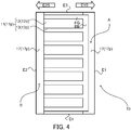
- FIG. 3 A perspective view of Fig. 3 illustrates a solar cell 10 using a silicon-made semiconductor substrate 15, and Fig. 4 is a plan view of Fig. 3 .
- the semiconductor substrate 15 includes two major surfaces 15S (15SU and 15SB). Therefore, in the present specification, in two major surfaces 15S, the major surface 15S on one surface side is defined as a surface 15SU, and the major surface 15S on the other surface side is defined as a back surface 15SB.
- one surface is described as a light reception side [a light receiving surface side] that actively receives light compared to the other surface, and the other surface that does not actively receive light is described as a non-light receiving backside [a back surface side].
- the solar cell 10 includes the semiconductor substrate 15, intrinsic semiconductor layers 16, conductivity type semiconductor layers 17 (a p-type semiconductor layer 17p and an n-type semiconductor layer 17n), and electrode layers 11 (a transparent oxide electrode layers 12 and a metal electrode layers 13). Note that, in the following description, for the sake of convenience, in members individually associated with the p-type semiconductor layer 17p or the n-type semiconductor layer 17n, "p" or "n” may be applied to the ends of the member reference numerals.
- the semiconductor substrate 15 may be a substrate formed of monocrystalline silicon (a silicon wafer), or may be a substrate formed of polycrystalline silicon.
- a monocrystalline silicon substrate will be described as an example.
- the conductive type of the semiconductor substrate 15 may be either an n-type monocrystalline silicon substrate containing impurities (for example, a phosphorus atom) that introduce an electron into a silicon atom, or may be a p-type monocrystalline silicon substrate containing impurities (for example, a boron atom) that introduce a hole into a silicon atom.
- impurities for example, a phosphorus atom
- p-type monocrystalline silicon substrate containing impurities for example, a boron atom
- the light receiving surface 15SU of two major surfaces 15SU and 15SB has a texture structure having mountains (protrusions) and valleys (depressions) formed, from the viewpoint of trapping received light.
- the texture structure an uneven surface
- the texture structure is formed by anisotropic etching to which a difference between an etching rate of a (100) surface of the semiconductor substrate 15 and an etching rate of a (111) surface is applied.
- the thickness of the semiconductor substrate 15 is less than or equal to 200 ⁇ m from the viewpoint of suppressing the amount of silicon that is used.
- a measurement direction in the case of measuring the thickness is a direction vertical to an average surface of the semiconductor substrate 15 (the average surface indicates a surface as the entire substrate that does not depend on the texture structure). Therefore, hereinafter, such a vertical direction, that is, a direction for measuring the thickness, will be described as a thickness direction for measuring film thicknesses of various layers.
- the thickness of the semiconductor substrate 15 is preferably greater than or equal to 50 ⁇ m, and is more preferably greater than or equal to 70 ⁇ m. Note that, in a case where the texture structure is formed on the major surface 15S of the semiconductor substrate 15, the thickness of the semiconductor substrate 15 is represented by a maximum distance between straight lines connecting vertexes of protrusions in a depression-protrusion structure on each of the light reception side and the backside.
- the silicon wafer may be used as the semiconductor substrate 15 by being cut.
- the solar cell 10 having a size smaller than that of the silicon wafer is obtained, and thus, a thin and flexible semiconductor substrate 15 is less likely to be damaged.
- a planar shape of the semiconductor substrate 15 is an approximately rectangular shape including four sides E1 to E4, and it is more preferable that the planar shape is an approximately oblong shape including long sides E1 and E2 and short sides E3 and E4.
- the "approximately rectangular shape” includes not only a complete rectangular shape (an oblong shape including a square shape) but also a shape in which at least one corner is missing, such as a shape in which at least one corner is rounded.
- the "approximately oblong shape” includes not only a complete oblong shape but also a shape in which at least one corner is missing, such as a shape in which at least one corner is rounded.
- the intrinsic semiconductor layers 16 (16p and 16n) individually directly cover both of the approximately rectangular major surfaces 15S (15SU and 15SB) of the semiconductor substrate 15, and thus perform surface passivation while suppressing impurity diffusion to the semiconductor substrate 15.
- the "intrinsic (i type)" semiconductor layer is not limited to a completely intrinsic layer that does not contain conductive impurities, and also includes a "weak n-type” or “weak p-type” substantially intrinsic layer containing a slight amount of n-type impurities or p-type impurities in a range in which a silicon-based layer is capable of functioning as an intrinsic layer.
- the shape and the area of the intrinsic semiconductor layer 16p are approximately identical to those of the major surface 15SU of the semiconductor substrate 15, and the shape and the area of the intrinsic semiconductor layer 16n are approximately identical to those of the major surface 15SB of the semiconductor substrate 15.
- the present invention is not limited thereto.
- the material of the intrinsic semiconductor layer 16 is not particularly limited, but an amorphous silicon-based thin film is preferable, a hydrogenated amorphous silicon-based thin film layer containing silicon and hydrogen is more preferable, as the material.
- a forming method of the intrinsic semiconductor layer 16 is not particularly limited, but a plasma chemical vapor deposition (CVD) method is preferable as the forming method.
- a substrate temperature is higher than or equal to 100°C and lower than or equal to 300°C
- a pressure is greater than or equal to 20 Pa and less than or equal to 2600 Pa
- a high-frequency power density is greater than or equal to 0.003 W/cm 2 and less than or equal to 0.5 W/cm 2 , as a condition for forming the thin film by the plasma CVD method.
- silicon-containing gas such as SiH4 and Si 2 H 6 , or a mixture of such gas and H 2 is preferable as raw material gas that is used for forming the thin film.
- Examples of the conductivity type semiconductor layers 17 include the p-type semiconductor layer 17p and the n-type semiconductor layer 17n.
- the p-type semiconductor layer 17p is formed on the approximately rectangular intrinsic semiconductor layer 16p that is formed on the major surface (the light receiving surface) 15SU of the semiconductor substrate 15 on the light reception side
- the n-type semiconductor layer 17n is formed on the approximately rectangular intrinsic semiconductor layer 16n that is formed on the major surface (the back surface) 15SB of the semiconductor substrate 15 on the backside.
- the electrode layers 11 are also individually formed on one surface side and the other surface side of the semiconductor substrate 15. For this reason, such a solar cell 10 is referred to as a double-sided electrode type solar cell 10.
- the shape and the area of the p-type semiconductor layer 17p are approximately identical to those of the intrinsic semiconductor layer 16p, and the major surface 15SU of the semiconductor substrate 15, and the shape and the area of the n-type semiconductor layer 17n are approximately identical to those of the intrinsic semiconductor layer 16n, and the major surface 15SB of the semiconductor substrate 15.
- the present invention is not limited thereto.
- a manufacturing method of the conductivity type semiconductor layer 13 is not particularly limited, but as with the intrinsic semiconductor layer 16, the plasma CVD method is preferable as the manufacturing method.
- the p-type semiconductor layer 17p is formed of a silicon layer to which a p-type dopant (boron or the like) is added.
- the p-type semiconductor layer include a p-type hydrogenated amorphous silicon layer, a p-type amorphous silicon carbide layer, or a p-type amorphous silicon oxide layer.
- the p-type semiconductor layer 17p is formed of amorphous silicon, from the viewpoint of suppressing the impurity diffusion or decreasing a series resistance.
- the p-type amorphous silicon carbide layer and the p-type amorphous silicon oxide layer are a low-refractive index layer with a wide gap, which is preferable from the viewpoint of reducing an optical loss.
- the n-type semiconductor layer 17n is formed of a silicon layer to which an n-type dopant (phosphorus or the like) is added. Note that, as with the p-type semiconductor layer 17p, it is preferable that the n-type semiconductor layer 17n is formed of an amorphous silicon layer.
- the electrode layers 11 individually cover the p-type semiconductor layer 17p and the n-type semiconductor layer 17n, and thus, are electrically connected to the semiconductor layers 17p and 17n. Accordingly, the electrode layers 11 function as a transport layer that guides a carrier generated in the p-type semiconductor layer 17p or the n-type semiconductor layer 17n.
- the electrode layers 11 are formed as a multilayer, and transparent oxide electrode layers 12 (12p and 12n) containing a transparent conductive oxide as a main component are formed as layers that are individually directly in contact with the p-type semiconductor layer 17p and the n-type semiconductor layer 17n.
- the "main component" indicates that the content of the substance is greater than or equal to 51 weight%, is preferably greater than or equal to 70 weight%, and is more preferably 90 weight%.
- the transparent oxide electrode layer 12 may be a single layer or a multilayer.
- the material of the transparent conductive oxide is not particularly limited, but examples of the material include zinc oxide or indium oxide, or a material in which various metal oxides, for example, titanium oxide, tin oxide, tungsten oxide, molybdenum oxide, and the like are added to indium oxide at greater than or equal to 1 weight% and less than or equal to 10 weight%.
- a doping agent such as Sn, W, As, Zn, Ge, Ca, Si, and C may be added to such a material.
- the thickness of the transparent oxide electrode layer 12 is greater than or equal to 10 nm and less than or equal to 140 nm, and examples of a forming method of the transparent oxide electrode layer 12 that is suitable for such a film thickness include a physical vapor deposition (PVD) method such as a sputtering method, a chemical vapor deposition (MOCVD) method using a reaction between an organic metal compound and oxygen or water, or the like.
- PVD physical vapor deposition
- MOCVD chemical vapor deposition
- the shape of the transparent oxide electrode layer 12p is an approximately rectangular shape that is identical to the shape of the p-type semiconductor layer 17p, but is formed to be smaller than the area of the p-type semiconductor layer 17p. Furthermore, the transparent oxide electrode layer 12p is formed such that a region [region] that is not covered with the transparent oxide electrode layer 12p is formed on one end side E 1S and the other end side E2S, one end side E 1S being one of the facing sides E1 and E2 of the semiconductor substrate 15, the other end side E2S being the other of the facing sides.
- the shape of the transparent oxide electrode layer 12n is the approximately rectangular shape that is identical to the shape of the n-type semiconductor layer 17n, but is formed to be smaller than the area of the n-type semiconductor layer 17n. Furthermore, the transparent oxide electrode layer 12n is formed such that a region [region] that is not covered with the transparent oxide electrode layer 12n is generated on one end side E1S and the other end side E2S of the semiconductor substrate 15.
- Such a transparent oxide electrode layer 12 is formed by using a lift-off method that is a partial coating method of a film mask. That is, in a case where a film mask having a patterned opening is used, the transparent oxide electrode layer 12 is formed in a portion overlapping the opening, and the transparent oxide electrode layer 12 is formed immediately below a non-opening portion, a conductive region in which the transparent oxide electrode layer 12 is formed and a region (a non-conductive region) in which the transparent oxide electrode layer is not formed are formed.
- the film formation of the transparent oxide electrode layer 12 is not limited to the lift-off method, and for example, may be a method of directly preparing a pattern by forming a film through a perforated metal such as a stencil mask, a method of forming the transparent oxide electrode layer 12 on the entire semiconductor layer 17, and then of removing the transparent oxide electrode layer 12 by partial etching (a subtractive method), or a method of directly applying a transparent electrode material only to a conductive region, and of forming a conductive layer (an additive method).
- the electrode layer 11 includes, in addition to a transparent oxide electrode layer for the p-type semiconductor layer 17p [a transparent oxide electrode layer for p-type] 12p and a transparent oxide electrode layer for the n-type semiconductor layer 17n [a transparent oxide electrode layer for n-type] 12n, the metal electrode layers 13 [a metal electrode layer for p-type 13p and a metal electrode layer for n-type 13n] are formed for each of the layers 12p and 12n.
- the metal electrode layer 13 is formed by directly stacking at least a part thereof on the surface side of the transparent oxide electrode layer 12, and is electrically connected to the transparent oxide electrode layer 12.
- the present invention is not limited thereto, but another layer may be interposed between both of the layers 12 and 13 insofar as the metal electrode layer 13 is electrically connected to the transparent oxide electrode layer 12.
- the material of the metal electrode layer 13 is not particularly limited, but examples of the material include silver, copper, aluminum, nickel, or the like.
- a conductive paste containing such a metal material and a binder resin may be the material of the metal electrode layer 13.
- Such a material is a light shielding material, and thus, the metal electrode layer 13 that is disposed on the light reception side of the solar cell 10 is formed into the shape of a thinned pattern.
- a comb-tooth type metal electrode layer 13p is exemplified.
- a portion that is a comb back is referred to as a bus bar part BB
- portions in which comb teeth are arranged along the length of the comb back while intersecting with (orthogonal to) the comb back are referred to as finger parts FG.
- the bus bar part BB is formed along a side on one end side E 1 (a long side direction) of the semiconductor substrate 15, and the finger parts FG extend along a short side direction (the short sides E3 and E4) intersecting with the long side direction and arranged along the long side direction, but the present invention is not limited thereto.
- the bus bar part BB extends from terminals of a plurality of finger parts FG on the surface of the transparent oxide electrode layer 12p, and reaches the p-type semiconductor layer 17p, but the present invention is not limited thereto.
- the metal electrode layer 13n has a planar shape having approximately the same size as that of the transparent oxide electrode layer 12n, and is formed to fall within the area of the transparent oxide electrode layer 12n.
- the metal electrode layer is not limited to such a planar electrode in a rectangular shape, but may be a comb-tooth type metal electrode layer even on the backside, as with the light reception side.
- the thickness of the metal electrode layers 13p and 13n is greater than or equal to 20 ⁇ m and less than or equal to 80 ⁇ m, and examples of a forming method of the metal electrode layer 13 that is suitable for such a film thickness include a printing method of performing ink jet printing or screen printing with respect to a conductive paste, or a plating method.
- the present invention is not limited thereto, but in the case of adopting a vacuum process, a vapor deposition method or a sputtering method may be adopted.
- an annealing treatment is performed in order for the passivation of each junction interface, and for the suppression of the occurrence of a defect level on the semiconductor layer and the interface thereof.
- the annealing treatment examples include a heating treatment in which a semiconductor substrate 15 on which each layer is disposed is put into an oven that is heated at higher than or equal to 150°C and lower than or equal to 200°C.
- the atmosphere in the oven may be the atmospheric air, but more effective annealing treatment is performed by using hydrogen or nitrogen.
- the annealing treatment may be rapid thermal annealing (RTA) treatment in which the semiconductor substrate 15 on which each layer is disposed is irradiated with an infrared ray by using an infrared heater.
- RTA rapid thermal annealing
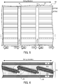
- the solar cell module 20 includes at least, the solar cell 10, a conductive adhesive agent 22, a sealing material 23 (a light reception side sealing material 23U and a backside sealing material 23B), a light reception side protective member 24, and a backside protective member 25.
- At least two solar cells 10 are included in the solar cell module 20, and the solar cells 10 are at least electrically connected through the conductive adhesive agent 22.
- the plurality of solar cells 10 connected in to the shape of a string is referred to as a solar cell string 21.
- the conductive adhesive agent 22 is interposed between the parts.
- the conductive adhesive agent 22 is interposed between the bus bar part BB that is a part of the metal electrode layer 13p of the first solar cell 10 and a part of the metal electrode layer 13n of the second solar cell 10, and thus electrically connects the solar cells 10.
- the solar cell module 20 includes one or more solar cell strings 21.
- first solar cell and the “second solar cell” indicate one and the other of two adjacent solar cells 10 and 10, in the solar cell string 21 formed of a plurality of solar cells 10.
- the solar cell 10 positioned in the center of three arranged solar cells 10 is the “second solar cell 10" in a case where the adjacent solar cell is the "first solar cell 10" on the other end side E2S (or one end side E1S), and is the "first solar cell 10" in a case where the adjacent solar cell is the "second solar cell 10" on one end side E1S (or the other end side E2S). That is, one solar cell 10 may be the "first solar cell", or may be the "second solar cell”.
- a deposition structure is formed in which a plurality of solar cells 10 are uniformly inclined in a certain direction as with a tiled roof.
- examples of the conductive adhesive agent 22 include a conductive adhesive paste.
- a conductive adhesive agent paste for example, is a paste-like adhesive agent in which conductive particles are dispersed in a thermosetting adhesive resin material such as an epoxy resin, an acrylic resin, or a urethane resin.
- a conductive adhesive film or an anisotropic conductive film that is formed into the shape of a film by dispersing conductive particles in a thermosetting adhesive resin material may be used.
- the sealing material 23 seals and protects the solar cell 10, and is interposed between the surface of the solar cell 10 on the light reception side and the light reception side protective member 24, and between the surface of the solar cell 10 on the backside and the backside protective member 25.
- the sealing material 23 covering the light reception side of the solar cell 10 may be referred to as the light reception side sealing material 23U
- the sealing material 23 covering the backside of the solar cell 10 may be referred to as the backside sealing material 23B in some cases.
- the shapes of the light reception side sealing material 23U and the backside sealing material 23B are not particularly limited, and examples of the shapes include a sheet shape. This is because in the sheet shape, the surface and the back surface of the planar solar cell 10 are easily covered.
- the material of the sealing material 23 is not particularly limited, but it is preferable that the material has properties of transmitting light (light transmissive properties).
- the material of the sealing material 23 has adhesive properties of allowing the solar cell 10, the light reception side protective member 24, and the backside protective member 25 to adhere with one another.
- Examples of such a material include a light transmissive resin such as an ethylene/vinyl acetate copolymer (EVA), an ethylene/ ⁇ -olefin copolymer, ethylene/vinyl acetate/triallyl isocyanurate (EVAT), polyvinyl butyrate (PVB), an acrylic resin, a urethane resin, or a silicone resin.
- a light transmissive resin such as an ethylene/vinyl acetate copolymer (EVA), an ethylene/ ⁇ -olefin copolymer, ethylene/vinyl acetate/triallyl isocyanurate (EVAT), polyvinyl butyrate (PVB), an acrylic resin, a urethane resin, or a silicone resin.
- EVA ethylene/vinyl acetate copolymer
- EVAT ethylene/vinyl acetate/triallyl isocyanurate
- PVB polyvinyl butyrate
- acrylic resin a ure
- the light reception side protective member 24 covers the surface of the solar cell 10 (the light receiving surface) through the light reception side sealing material 23U, and protects the solar cell 10.
- the shape of the light reception side protective member 24 is not particularly limited, but a plate shape or a sheet shape is preferable from the viewpoint of indirectly cover the planar light receiving surface.
- the material of the light reception side protective member 24 is not particularly limited, but as with the sealing material 23, a material resistant to ultraviolet light while having light transmissive properties is preferable, and examples of the material include glass, or a transparent resin such as an acrylic resin or a polycarbonate resin.
- the surface of the light reception side protective member 24 may be processed into a depression-protrusion shape, or may be covered with an antireflection coating layer. This is because the light reception side protective member 24 above is less likely to reflect received light, and thus, guides more light to the solar cell 10.
- the backside protective member 25 covers the back surface of the solar cell 10 through the backside sealing material 23B, and protects the solar cell 10.
- the shape of the backside protective member 25 is not particularly limited, but a plate shape or a sheet shape is preferable from the viewpoint of indirectly covering the planar back surface, as with the light reception side protective member 24.
- the material of the backside protective member 25 is not particularly limited, but a material preventing the infiltration of water or the like (having high water barrier properties) is preferable.
- the material include a laminated body of a resin film such as polyethylene terephthalate (PET), polyethylene (PE), an olefin-based resin, a fluorine-containing resin, or a silicone-containing resin, and a metal foil such as an aluminum foil.
- a manufacturing method of the solar cell module 20 is not particularly limited.
- the backside protective member 25, the backside sealing material 23B, the solar cell 10 (the solar cell string 21), the light reception side sealing material 23U, and the light reception side protective member 24 are overlapped in this order, are heated and pressurized at a predetermined temperature and a predetermined pressure, and thus, are sealed, by using a laminator or the like performing evacuation.
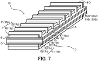
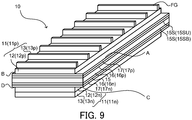
- the solar cell string 21 that is used in the solar cell module 20 as described above will be described in detail by using Figs. 3 and 4 , in addition to Fig. 1 that is an enlarged view of a circle portion with a dashed line of Fig. 6 .
- the solar cell 10 of the solar cell string 21 includes the semiconductor substrate 15, and the p-type semiconductor layer 17p and the transparent oxide electrode layer for p-type 12p corresponding to the p-type semiconductor layer 17p, for example, on the light receiving surface 15SU side [the light receiving surface side] that is one surface side of the major surfaces 15S of the semiconductor substrate 15.
- the solar cell 10 includes the n-type semiconductor layer 17n and the transparent oxide electrode layer for n-type 12n corresponding to the n-type semiconductor layer 17n, for example, on the back surface 15SB side [the back surface side] that is the other surface side of the major surface 15S of the semiconductor substrate 15.
- the conductive adhesive agent 22 is interposed between the parts and electrically connects both of the solar cells 10. Then, the region A is shielded by the second solar cell 10.
- one end side E1S of both facing sides in one solar cell 10 is shielded by the other end side E2S of both of the facing sides in another solar cell 10.
- a dark current may be generated.
- the recombination of the carrier is more likely to occur, and a dark current is also easily generated, compared to the central portion of the semiconductor substrate 15, due to film formation around a side opposite to a film formation surface of the p-type semiconductor layer 17p or the n-type semiconductor layer 17n, a mechanical damage, or the like.
- the region A is designed to be wide. For this reason, even in a case where a dark current is generated in pn junction in the region A, there is no transparent oxide electrode layer for p-type, and thus, the dark current is not collected. As a result thereof, a decrease in an operating point voltage of the solar cell module 20 due to the dark current is less likely to occur, and the output of the solar cell module 20 does not decrease.
- the transparent oxide electrode layer for p-type 12p most of the collection of the carriers generated in the semiconductor substrate 15 is performed by the transparent oxide electrode layer for p-type 12p, and thus, it is preferable that the area of the transparent oxide electrode layer for p-type 12p is large except for the region A.
- the length of the region B along a direction connecting one end side E1S to the other end side E2S is less than 2 times the thickness of the semiconductor substrate 15 (note that, in Fig. 4 , the direction is a direction parallel to the sides E3 and E4 of the semiconductor substrate 15, and the direction is referred to as a string direction from a direction in which the solar cell 10 forms the solar cell string 21).
- the solar cell module 20 on which the solar cell 10 is mounted improves the output while suppressing the influence of a dark current.
- a region facing the region B with the semiconductor substrate 15 as a boundary is defined as a "region D". Then, it is preferable that the area of the region D is smaller than or equal to the area of the region B.
- the region D may be narrow (that is, the transparent oxide electrode layer for n-type 12n may be wide). Note that, it is sufficient that the area of the region D is smaller than or equal to the area of the region B, and thus, the region D may not exist.
- a region facing the region A with the semiconductor substrate 15 as a boundary is defined as a "region C". Then, it is preferable that the area of the region C is larger than the area of the region B.
- the conductive adhesive agent 22 is disposed in the region A or in the vicinity thereof by coating or the like. For this reason, in the connection of the solar cells 10, the conductive adhesive agent 22 may not only spread to the region A, but also wrap around the region C positioned on a side opposite to the over the region A, over the end portion of the semiconductor substrate 15.
- the region C is designed to be wide, and thus, even in a case where the conductive adhesive agent 22 extends to the region C, the conductive adhesive agent 22 is less likely to contact with the transparent oxide electrode layer for n-type 12n. Therefore, a leakage due to the conductive adhesive agent 22 that bridges a gap between one end side E1S of the transparent oxide electrode layer for p-type 12p and one end side E1S of the transparent oxide electrode layer for n-type 12n is less likely to occur.
- the region A to the region D described above are not limited to the solar cell module 20 in which the p-type semiconductor layer 17p is disposed on the light reception side, and the n-type semiconductor layer 17n is disposed on the backside, as illustrated in Fig. 1 . That is, the same applies to the solar cell module 20 using the solar cell 10 in which the n-type semiconductor layer 17n is disposed on the light reception side, and the p-type semiconductor layer 17p is disposed on the backside, as illustrated in Fig. 2 .
- the conductive adhesive agent 22 is interposed between the parts, and electrically connects both of the solar cells 10. Then, the region C is shielded by the second solar cell 10.
- the solar cell 10 in the solar cell module 20 also includes the semiconductor substrate 15, the p-type semiconductor layer 17p and the transparent oxide electrode layer for p-type 12p corresponding to the p-type semiconductor layer 17p, for example, on the back surface 15SB side that is one surface side of the major surfaces 15S of the semiconductor substrate 15.
- the solar cell 10 includes the n-type semiconductor layer 17n and the transparent oxide electrode layer for n-type 12n corresponding to the n-type semiconductor layer 17n, for example, on the light receiving surface 15SU side that is the other surface side of the major surfaces 15S of the semiconductor substrate 15.
- the solar cell module 20 on which such a solar cell 10 is mounted even in a case where a dark current is generated in pn junction of the region A on the back surface 15SB side, there is no transparent oxide electrode layer for p-type, and thus, the dark current is not collected. As a result thereof, a decrease in the operating point voltage of the solar cell module 20 due to the dark current is less likely to occur, and the output of the solar cell module 20 does not decrease.
- the length of the region B along the direction connecting one end side E1S to the other end side E2S (the string direction) is less than 2 times the thickness of the semiconductor substrate 15.
- the p-type semiconductor layer 17p is disposed on the back surface 15SB side, and thus, even in a case where a pn junction surface is not directed towards the light reception side, most of the collection of the carriers generated in the semiconductor substrate 15 is performed by the transparent oxide electrode layer for p-type 12p, and therefore, it is preferable that the area of the transparent oxide electrode layer for p-type is large except for the region A.
- a region facing the region B with the semiconductor substrate 15 as a boundary is defined as a "region D". Then, it is preferable that the area of the region D is smaller than or equal to the area of the region B.
- a potential difference between the transparent oxide electrode layer for n-type 12n and the semiconductor substrate 15 is less than a potential difference between the transparent oxide electrode layer for p-type 12p and the semiconductor substrate 15, and thus, a dark current is less likely to flow through the transparent oxide electrode layer for n-type 12n, and the region D may be narrow.
- the area of the region D is smaller than or equal to the area of the region B, and thus, the region D may not exist. That is, the entire other end side E2S on the light receiving surface 15SU side may be covered with the transparent oxide electrode layer for n-type 12n. Therefore, the transparent oxide electrode layer for n-type 12n, for example, is capable of exhibiting the function of an antireflection layer, and thus, the appearance of the solar cell module 20 is improved.
- a region facing the region A with the semiconductor substrate 15 as a boundary is defined as a "region C". Then, it is preferable that the area of the region C is larger than the area of the region B.
- the conductive adhesive agent 22 is disposed in the region C or in the vicinity thereof. For this reason, in the connection of the solar cells 10, the conductive adhesive agent 22 may not only spread to the region C, but also wrap around the region A positioned on a side opposite to the region C, over the end portion of the semiconductor substrate 15.
- the region C is designed to be wide, and thus, the conductive adhesive agent 22 wraps around the region C to the region A, and thus, is less likely to advance to the p-type semiconductor layer 17p. Therefore, a leakage due to the conductive adhesive agent 22 that bridges a gap between one end side E1S of the transparent oxide electrode layer for p-type 12p and one end side E1S of the transparent oxide electrode layer for n-type 12n is less likely to occur.
- the solar cell module 20 is formed of the solar cell 10 in which the p-type semiconductor layer 17p is disposed on the light receiving surface 15SU side that is one surface, and the n-type semiconductor layer 17n is disposed on the back surface 15SB side that is the other surface side, in the solar cell 10, it is preferable that at least a part of the region A is covered with a part of the metal electrode layer for p-type 13p that is electrically connected to the transparent oxide electrode layer for p-type 12p, from the viewpoint of preventing the leakage between the p-type semiconductor layer 17p and the n-type semiconductor layer 17n.
- a part of the metal electrode layer for p-type 13p extends to the region A, that is, the end of the semiconductor substrate 15 on one end side E1S, and thus, the conductive adhesive agent 22 can be disposed in the portion. Then, in a case where the region A is covered with the solar cell 10, the conductive adhesive agent 22 is hidden by the solar cell 10. As a result thereof, in the solar cell module 20, the conductive adhesive agent 22 does not protrude to the light receiving surface 15SU side over a shielding region, and thus, a shadow loss due to the conductive adhesive agent 22 is suppressed.
- the region A is shielded by the second solar cell 10, and thus, a part of the metal electrode layer for p-type 13p that extends to the region A is also covered with the solar cell 10.
- the area of the metal electrode layer for n-type 13n that is electrically connected to the transparent oxide electrode layer for n-type 12n by covering the transparent oxide electrode layer for n-type 12n is smaller than or equal to the area of the transparent oxide electrode layer for n-type 13n, and does not overlap the region C.
- a part of the region C on an opposite side of the region A is not covered with a part of the metal electrode layer for n-type 13p. Then, for example, even in a case where the conductive adhesive agent 22 spreads to the region A, and wraps around the region C over the end portion of the semiconductor substrate 15, the conductive adhesive agent is less likely to reach the metal electrode layer for n-type 13n. For this reason, a leakage due to the conductive adhesive agent 22 that bridges a gap between one end side E1S of the metal electrode layer for p-type 13p and one end side E1S of the metal electrode layer for n-type 13n is less likely to occur.
- the solar cell module 20 including the solar cell 10 in which the n-type semiconductor layer 17n is disposed on the light receiving surface 15SU side that is the other surface, and the p-type semiconductor layer 17p is disposed on the back surface 15SB side that is one surface side it is preferable to adopt the same configuration as described above. That is, in such a solar cell 10, it is preferable that a part of the region C is covered with a part of the metal electrode layer for n-type 13n that is electrically connected to the transparent oxide electrode layer for n-type 12n.
- a part of the metal electrode layer for n-type 13n extends to the region C, that is, the end of the semiconductor substrate 15 on one end side E1S, and thus, the conductive adhesive agent 22 can be disposed in the portion. Then, in a case where the region C is covered with the solar cell 10, the conductive adhesive agent 22 is hidden by the solar cell 10, and a shadow loss due to the conductive adhesive agent 22 is suppressed, similarly to the above.
- the region C is shielded by the second solar cell 10, and thus, a part of the metal electrode layer for n-type 13n that extends to the region C is also covered with the solar cell 10.
- the area of the metal electrode layer for p-type 13p that is electrically connected to the transparent oxide electrode layer for p-type 12p by covering the transparent oxide electrode layer for p-type 12p is smaller than or equal to the area of the transparent oxide electrode layer for p-type 12p, and does not overlap the region A.
- a part of the region A on an opposite side of the region C is not covered with a part of the metal electrode layer for p-type 13p. For this reason, for example, even in a case where the conductive adhesive agent 22 spreads to the region C, and wraps around the region A over the end portion of the semiconductor substrate 15, the conductive adhesive agent is less likely to reach the metal electrode layer for p-type 13p. For this reason, a leakage due to the conductive adhesive agent 22 that bridges a gap between one end side E1S of the metal electrode layer for n-type 13n and one end side E1S of the metal electrode layer for p-type 13p is less likely to occur.
- the present invention is not limited thereto.
- the metal electrode layer 13p may include only the finger part FG.
- the conductive adhesive agent 22 may be disposed in the position of the bus bar part BB illustrated in Fig. 3 , instead of the bus bar part BB.
- the finger part FG may fall within the surface of the transparent oxide electrode layer 12.
- the conductive adhesive agent 22 may be disposed to connect the respective finger parts FG, and may be used instead of the bus bar part BB illustrated in Fig. 3 .
- the conductive adhesive agent 22 that is used instead of the bus bar part BB may be disposed on the transparent oxide electrode layer 12, and may not be disposed on the conductivity type semiconductor layer 17.
- bus bar part BB or the conductive adhesive agent 22 that is used instead of the bus bar part are in the shape of one line, but the present invention is not limited thereto, and the bus bar part BB or the conductive adhesive agent 22 may be in the shape of a plurality of lines, or may be in a non-linear shape.
- a 6-inch n-type monocrystalline silicon substrate having a thickness of 200 ⁇ m was washed with acetone, and then, was immersed in an aqueous solution of HF of 2 weight% for 5 minutes, a silicon oxide layer on the surface was removed, and rinsing with ultrapure water was performed twice. After that, the semiconductor substrate was immersed in an aqueous solution of KOH/isopropyl alcohol of 5/15 weight% that was retained at 75°C for 15 minutes. Next, the semiconductor substrate was immersed in an aqueous solution of HF of 2 weight% for 5 minutes, was rinsed with ultrapure water twice, and was dried at a normal temperature.
- the surface of the dried semiconductor substrate was observed with an atomic force microscope (AFM), and as a result thereof, a texture structure in the shape of a quadrangular pyramid was formed on both surfaces, and arithmetic average roughness thereof was 2100 nm.
- AFM atomic force microscope
- the surface of the monocrystalline silicon substrate in which the texture has been formed was immersed in an aqueous solution of HCl of 5% at 70°C for 5 minutes, and an alkaline component remaining on the surface was neutralized. After that, the surface was washed for 10 minutes by using ozone water of 15 ppm, and was immersed in an aqueous solution of HF of 5% for 2 minutes, and thus, an ozone oxide film was removed.
- Examples 1 and 2 and Comparative Example 1 described below the semiconductor substrate described above was used. Specifically, a p-type semiconductor layer and an n-type semiconductor layer were formed on the semiconductor substrate, a transparent oxide electrode layer and a metal electrode layer were formed thereon, and the semiconductor substrate was divided at a desired position, by using laser. For this reason, an electrode layer was formed in accordance with a plurality of divided pieces formed from a large-sized semiconductor substrate. In addition, the divided pieces (solar cells) were connected by using a conductive adhesive agent, in a singling method, and thus, a solar cell string was obtained. Then, a solar cell module was prepared by using the solar cell string.
- the details will be described.
- a large-sized semiconductor substrate was introduced into a CVD device, an i-layer amorphous silicon layer of 4 nm was formed on one surface, as an intrinsic semiconductor layer, and a p-type amorphous silicon layer of 5 nm was formed thereon, as the p-type semiconductor layer.
- a substrate temperature was 180°C
- a pressure was 130 Pa
- a flow ratio of SiH 4 /H 2 was 2/10
- an input power density was 0.03 W/cm 2 .
- a substrate temperature was 190°C
- a pressure was 130 Pa
- a flow ratio of SiH 4 /H 2 /B 2 H 6 was 1/10/3
- an input power density was 0.04 W/cm 2 .
- gas in which the concentration of B 2 H 6 was diluted by H 2 to 5000 ppm was used as B 2 H 6 gas described above.
- an i-layer amorphous silicon layer of 5 nm was formed on the other surface of the semiconductor substrate, as the intrinsic semiconductor layer, and an n-type amorphous silicon layer of 10 nm was formed thereon, as the n-type semiconductor layer.
- the film formation condition of the intrinsic semiconductor layer is as described above.
- a substrate temperature was 180°C
- a pressure was 60 Pa
- a flow ratio of SiH 4 /PH 3 was 1/2
- an input power density was 0.02 W/cm 2 .
- gas in which the concentration of PH 3 was diluted by H 2 to 5000 ppm was used as PH 3 gas described above.
- the semiconductor substrate including the conductivity type semiconductor layer was sent to a sputtering chamber, an ITO layer of 120 nm was formed on the p-type semiconductor layer and the n-type semiconductor layer, as a transparent electrode layer. Note that, a region A to a region D were formed by a lift-off method using a film mask.
- the length of the regions A and C along a string direction connecting one end side to the other end side, from the end of the solar cell on one end side was set to 1100 ⁇ m.
- the length of the regions B and D along a string direction connecting the other end side to one end side, from the end of the solar cell on the other end side was set to 150 ⁇ m.
- a flexible resin film formed of polypropylene was used as the film mask.
- a biaxially stretched film was used as the film mask, from the viewpoint of a strength, heat resistance, dimensional stability, or the like.
- the semiconductor substrate including the transparent oxide electrode layer was sent to a printing chamber, and was coated with a silver paste by screen printing, and thus, a metal electrode layer was formed.
- comb-tooth type metal electrode layers were formed on the transparent electrode layers on a light reception side and a backside.
- the metal electrode layer on the light reception side was approximately orthogonal to a finger part and a bus bar electrode.
- the width of the finger part of the light reception side was approximately 50 ⁇ m
- an interval (a pitch) therebetween was approximately 1800 ⁇ m
- the width of the finger part on the backside was approximately 50 ⁇ m
- an interval therebetween was approximately 500 ⁇ m.
- the semiconductor substrate including the electrode layer described above was sent to a laser chamber, and was cut by using a laser device, and thus, a solar cell having an approximately oblong shape was prepared. Note that, laser was incident from a formation surface side of the n-type semiconductor layer. In addition, the position of the laser was adjusted to a division position that was set at the time of forming the transparent oxide electrode layer.
- the solar cell was sent to a dispenser chamber, the conductive adhesive agent was applied to the bus bar part in a region of a first solar cell to be superimposed, by using a dispenser, a second solar cell was overlapped with the first solar cell, and the first solar cell and the second solar cell were joined by thermal compression bonding. Such junction using the overlap was repeated by using a total of 34 solar cells.
- a solar cell string was prepared in which 34 solar cells were electrically connected in series. Note that, as a thermal compression bonding condition, a temperature was 150°C, a time was 20 minutes, and a pressure was 5 MPa.
- the solar cell string was sent to a sealing chamber, a light reception side sealing material, the solar cell string, a backside sealing material, and a backside protective member were laminated in this order, on a light reception side protective material, and the solar cell string was sealed, and thus, a solar cell module was prepared.
- 10 solar cell strings were arranged in 5 parallels ⁇ 2 series (a total of 340 solar cells), and thus, an assembly of the solar cell strings was obtained.
- modularization was performed such that the p-type semiconductor layer of each of the solar cells was directed towards the light reception side.
- the p-type semiconductor layer was disposed on the light receiving surface side, and the n-type semiconductor layer was disposed on the back surface side in the solar cell module of Example 1 while in Example 2, the direction was reversed, that is, the n-type semiconductor layer was disposed on the light receiving surface side, and the p-type semiconductor layer was disposed on the back surface side.
- the length of the region A was 1100 ⁇ m
- the length of the region B was 150 ⁇ m
- the region C and the region D were not formed, that is, the transparent oxide electrode layer was formed on the entire surface of the n-type semiconductor layer on the light receiving surface side.
- Comparative Example 1 in the solar cell module of Example 1, only the transparent oxide electrode layer was changed. Specifically, the transparent oxide electrode layer was formed on the entire surface of the conductivity type semiconductor layer of the solar cell without using the film mask.
- Example 1 From Table 1, it was determined that the output was higher in Example 1 and Example 2 than in Comparative Example 1. It is considered that this is because in both of the examples, a dark current of a shield portion of the solar cell due to the singling method was reduced, and thus, a diode loss in the solar cell was reduced, and thus, the fill factor (FF) was improved.
- FF fill factor
- Comparative Example 1 it is considered that the transparent oxide electrode layer is formed on the entire surface of the conductivity type semiconductor layer, and thus, it is considered that a leakage occurs due to the reattachment of a residue, and fusion droop of the transparent oxide electrode layer, at the time of being divided by laser irradiation.
- a division portion of the laser irradiation is a region in which the transparent oxide electrode layer is not formed. For this reason, a leakage does not occur as with Comparative Example 1, and thus, it is considered that output properties are improved.
Landscapes
- Photovoltaic Devices (AREA)
- Life Sciences & Earth Sciences (AREA)
- Engineering & Computer Science (AREA)
- Sustainable Energy (AREA)
Applications Claiming Priority (2)
| Application Number | Priority Date | Filing Date | Title |
|---|---|---|---|
| JP2017209637 | 2017-10-30 | ||
| PCT/JP2018/034222 WO2019087590A1 (ja) | 2017-10-30 | 2018-09-14 | 両面電極型太陽電池および太陽電池モジュール |
Publications (2)
| Publication Number | Publication Date |
|---|---|
| EP3664155A1 true EP3664155A1 (de) | 2020-06-10 |
| EP3664155A4 EP3664155A4 (de) | 2020-07-08 |
Family
ID=66331616
Family Applications (1)
| Application Number | Title | Priority Date | Filing Date |
|---|---|---|---|
| EP18873145.9A Pending EP3664155A4 (de) | 2017-10-30 | 2018-09-14 | Doppelseitige elektrodenartige solarzelle und solarzellenmodul |
Country Status (6)
| Country | Link |
|---|---|
| US (1) | US11404593B2 (de) |
| EP (1) | EP3664155A4 (de) |
| JP (1) | JPWO2019087590A1 (de) |
| CN (1) | CN111095572B (de) |
| TW (1) | TW201931613A (de) |
| WO (1) | WO2019087590A1 (de) |
Families Citing this family (4)
| Publication number | Priority date | Publication date | Assignee | Title |
|---|---|---|---|---|
| JP2022002230A (ja) * | 2018-09-21 | 2022-01-06 | 株式会社カネカ | 太陽電池セル、太陽電池デバイスおよび太陽電池モジュール |
| CN115398652B (zh) | 2020-03-30 | 2025-06-10 | 株式会社钟化 | 电池单元集合体、电池单元集合体的制造方法、太阳电池单元、及太阳电池单元的制造方法 |
| JP2022025933A (ja) * | 2020-07-30 | 2022-02-10 | 株式会社カネカ | 太陽電池ストリング |
| CN116503425A (zh) * | 2023-05-18 | 2023-07-28 | 阳光智维科技股份有限公司 | 组串分割方法、装置、设备及介质 |
Family Cites Families (16)
| Publication number | Priority date | Publication date | Assignee | Title |
|---|---|---|---|---|
| JPH11186577A (ja) | 1997-12-19 | 1999-07-09 | Dainippon Printing Co Ltd | 薄膜太陽電池とその形成方法 |
| JP4194379B2 (ja) * | 2003-01-22 | 2008-12-10 | 三洋電機株式会社 | 光起電力装置 |
| ES2365904T3 (es) | 2004-01-13 | 2011-10-13 | Sanyo Electric Co., Ltd. | Dispositivo fotovoltaico. |
| JP4222991B2 (ja) * | 2004-01-13 | 2009-02-12 | 三洋電機株式会社 | 光起電力装置 |
| MY168566A (en) * | 2012-10-02 | 2018-11-13 | Kaneka Corp | Method for manufacturing crystalline silicon solar cell, method for manufacturing solar cell module, crystalline silicon solar cell, and solar cell module |
| WO2014132312A1 (ja) * | 2013-02-26 | 2014-09-04 | 三洋電機株式会社 | 太陽電池モジュールおよび太陽電池モジュールの製造方法 |
| JP6141670B2 (ja) * | 2013-03-29 | 2017-06-07 | 株式会社カネカ | 太陽電池の製造方法 |
| JP2015037002A (ja) * | 2013-08-09 | 2015-02-23 | 株式会社フジクラ | 電極、及び、これを有する色素増感太陽電池素子 |
| US9608140B2 (en) * | 2013-10-30 | 2017-03-28 | Kyocera Corporation | Solar cell and solar cell module |
| JP6360340B2 (ja) * | 2014-03-31 | 2018-07-18 | 株式会社カネカ | 太陽電池モジュールの製造方法 |
| US10593820B2 (en) * | 2014-03-31 | 2020-03-17 | Kaneka Corporation | Solar cell module and method for manufacturing same |
| TWI676299B (zh) * | 2014-10-06 | 2019-11-01 | 日商鐘化股份有限公司 | 太陽能電池及太陽能電池模組、以及太陽能電池及太陽能電池模組之製造方法 |
| EP3096360A1 (de) * | 2015-05-20 | 2016-11-23 | Lg Electronics Inc. | Solarzelle und solarzellenmodul |
| EP3182468B1 (de) * | 2015-12-18 | 2025-10-29 | JingAo Solar Co., Ltd. | Verfahren zur herstellung einer solarzelle |
| US20170256661A1 (en) * | 2016-03-02 | 2017-09-07 | Solarcity Corporation | Method of manufacturing photovoltaic panels with various geometrical shapes |
| WO2017179317A1 (ja) * | 2016-04-13 | 2017-10-19 | 株式会社カネカ | 結晶シリコン系太陽電池およびその製造方法、ならびに太陽電池モジュール |
-
2018
- 2018-09-14 WO PCT/JP2018/034222 patent/WO2019087590A1/ja not_active Ceased
- 2018-09-14 EP EP18873145.9A patent/EP3664155A4/de active Pending
- 2018-09-14 JP JP2019549937A patent/JPWO2019087590A1/ja active Pending
- 2018-09-14 CN CN201880058161.2A patent/CN111095572B/zh active Active
- 2018-10-18 TW TW107136680A patent/TW201931613A/zh unknown
-
2020
- 2020-02-28 US US16/805,016 patent/US11404593B2/en active Active
Also Published As
| Publication number | Publication date |
|---|---|
| WO2019087590A1 (ja) | 2019-05-09 |
| US20200203545A1 (en) | 2020-06-25 |
| US11404593B2 (en) | 2022-08-02 |
| CN111095572B (zh) | 2023-09-08 |
| TW201931613A (zh) | 2019-08-01 |
| JPWO2019087590A1 (ja) | 2020-11-12 |
| CN111095572A (zh) | 2020-05-01 |
| EP3664155A4 (de) | 2020-07-08 |
Similar Documents
| Publication | Publication Date | Title |
|---|---|---|
| US10593820B2 (en) | Solar cell module and method for manufacturing same | |
| EP3540785B1 (de) | Verfahren zur herstellung einer solarzelle | |
| CN103999242B (zh) | 晶体硅太阳能电池、太阳能电池模块及其制造方法 | |
| US11404593B2 (en) | Double-sided electrode type solar cell and solar cell module | |
| US10985289B2 (en) | Solar cell and solar cell module | |
| US11251319B2 (en) | Solar cell | |
| US10453981B2 (en) | Solar cell, solar cell module, method for manufacturing solar cell, and method for manufacturing solar cell module | |
| EP2136413A2 (de) | Photovoltaische Vorrichtung | |
| JP7353272B2 (ja) | 太陽電池デバイスおよび太陽電池デバイスの製造方法 | |
| JP6334871B2 (ja) | 太陽電池モジュール | |
| WO2019189267A1 (ja) | 太陽電池セルの製造方法、太陽電池モジュールの製造方法、太陽電池セル、および、太陽電池モジュール | |
| US8598447B2 (en) | Photoelectric conversion device | |
| JP7043308B2 (ja) | 太陽電池の製造方法、および、太陽電池 | |
| EP2806465B1 (de) | Solarzelle und Verfahren zu ihrer Herstellung | |
| JP6995828B2 (ja) | 太陽電池モジュール | |
| WO2014050193A1 (ja) | 光電変換モジュール | |
| JP6285713B2 (ja) | 結晶シリコン系太陽電池および太陽電池モジュール | |
| EP2618386B1 (de) | Beidseitige Solarzelle | |
| CN113330584B (zh) | 太阳能电池制造用基板托盘及太阳能电池的制造方法 | |
| WO2025204281A1 (ja) | タンデム型太陽電池セル、および、タンデム型太陽電池セルの製造方法 | |
| CN118476035A (zh) | 太阳能电池器件及太阳能电池模块 | |
| WO2025204282A1 (ja) | タンデム型太陽電池セル、および、タンデム型太陽電池セルの製造方法 | |
| KR102233886B1 (ko) | 태양전지 모듈 | |
| CN117957933A (zh) | 太阳能电池器件以及太阳能电池模块 | |
| TW202539463A (zh) | 光伏打裝置 |
Legal Events
| Date | Code | Title | Description |
|---|---|---|---|
| STAA | Information on the status of an ep patent application or granted ep patent |
Free format text: STATUS: THE INTERNATIONAL PUBLICATION HAS BEEN MADE |
|
| PUAI | Public reference made under article 153(3) epc to a published international application that has entered the european phase |
Free format text: ORIGINAL CODE: 0009012 |
|
| STAA | Information on the status of an ep patent application or granted ep patent |
Free format text: STATUS: REQUEST FOR EXAMINATION WAS MADE |
|
| 17P | Request for examination filed |
Effective date: 20200303 |
|
| AK | Designated contracting states |
Kind code of ref document: A1 Designated state(s): AL AT BE BG CH CY CZ DE DK EE ES FI FR GB GR HR HU IE IS IT LI LT LU LV MC MK MT NL NO PL PT RO RS SE SI SK SM TR |
|
| AX | Request for extension of the european patent |
Extension state: BA ME |
|
| A4 | Supplementary search report drawn up and despatched |
Effective date: 20200609 |
|
| RIC1 | Information provided on ipc code assigned before grant |
Ipc: H01L 31/0224 20060101AFI20200603BHEP Ipc: H01L 31/0747 20120101ALI20200603BHEP Ipc: H01L 31/05 20140101ALI20200603BHEP Ipc: H01L 31/043 20140101ALI20200603BHEP |
|
| DAV | Request for validation of the european patent (deleted) | ||
| DAX | Request for extension of the european patent (deleted) | ||
| STAA | Information on the status of an ep patent application or granted ep patent |
Free format text: STATUS: EXAMINATION IS IN PROGRESS |
|
| 17Q | First examination report despatched |
Effective date: 20220628 |