EP3664295B1 - Commande de commutateur à deux niveaux pour empêcher un effet d'avalanche pour un commutateur de redressement synchrone dans un convertisseur de puissance fonctionnant en mode rafale à faible puissance - Google Patents
Commande de commutateur à deux niveaux pour empêcher un effet d'avalanche pour un commutateur de redressement synchrone dans un convertisseur de puissance fonctionnant en mode rafale à faible puissance Download PDFInfo
- Publication number
- EP3664295B1 EP3664295B1 EP19212827.0A EP19212827A EP3664295B1 EP 3664295 B1 EP3664295 B1 EP 3664295B1 EP 19212827 A EP19212827 A EP 19212827A EP 3664295 B1 EP3664295 B1 EP 3664295B1
- Authority
- EP
- European Patent Office
- Prior art keywords
- switch
- driver
- pull
- power
- voltage
- Prior art date
- Legal status (The legal status is an assumption and is not a legal conclusion. Google has not performed a legal analysis and makes no representation as to the accuracy of the status listed.)
- Active
Links
Images



Classifications
-
- H—ELECTRICITY
- H02—GENERATION; CONVERSION OR DISTRIBUTION OF ELECTRIC POWER
- H02M—APPARATUS FOR CONVERSION BETWEEN AC AND AC, BETWEEN AC AND DC, OR BETWEEN DC AND DC, AND FOR USE WITH MAINS OR SIMILAR POWER SUPPLY SYSTEMS; CONVERSION OF DC OR AC INPUT POWER INTO SURGE OUTPUT POWER; CONTROL OR REGULATION THEREOF
- H02M3/00—Conversion of DC power input into DC power output
- H02M3/22—Conversion of DC power input into DC power output with intermediate conversion into AC
- H02M3/24—Conversion of DC power input into DC power output with intermediate conversion into AC by static converters
- H02M3/28—Conversion of DC power input into DC power output with intermediate conversion into AC by static converters using discharge tubes with control electrode or semiconductor devices with control electrode to produce the intermediate AC
- H02M3/325—Conversion of DC power input into DC power output with intermediate conversion into AC by static converters using discharge tubes with control electrode or semiconductor devices with control electrode to produce the intermediate AC using devices of a triode or a transistor type requiring continuous application of a control signal
- H02M3/335—Conversion of DC power input into DC power output with intermediate conversion into AC by static converters using discharge tubes with control electrode or semiconductor devices with control electrode to produce the intermediate AC using devices of a triode or a transistor type requiring continuous application of a control signal using semiconductor devices only
- H02M3/33569—Conversion of DC power input into DC power output with intermediate conversion into AC by static converters using discharge tubes with control electrode or semiconductor devices with control electrode to produce the intermediate AC using devices of a triode or a transistor type requiring continuous application of a control signal using semiconductor devices only having several active switching elements
- H02M3/33576—Conversion of DC power input into DC power output with intermediate conversion into AC by static converters using discharge tubes with control electrode or semiconductor devices with control electrode to produce the intermediate AC using devices of a triode or a transistor type requiring continuous application of a control signal using semiconductor devices only having several active switching elements having at least one active switching element at the secondary side of an isolation transformer
- H02M3/33592—Conversion of DC power input into DC power output with intermediate conversion into AC by static converters using discharge tubes with control electrode or semiconductor devices with control electrode to produce the intermediate AC using devices of a triode or a transistor type requiring continuous application of a control signal using semiconductor devices only having several active switching elements having at least one active switching element at the secondary side of an isolation transformer having a synchronous rectifier circuit or a synchronous freewheeling circuit at the secondary side of an isolation transformer
-
- H—ELECTRICITY
- H03—ELECTRONIC CIRCUITRY
- H03K—PULSE TECHNIQUE
- H03K17/00—Electronic switching or gating, i.e. not by contact-making and –breaking
- H03K17/16—Modifications for eliminating interference voltages or currents
- H03K17/161—Modifications for eliminating interference voltages or currents in field-effect transistor switches
- H03K17/162—Modifications for eliminating interference voltages or currents in field-effect transistor switches without feedback from the output circuit to the control circuit
- H03K17/163—Soft switching
- H03K17/164—Soft switching using parallel switching arrangements
-
- H—ELECTRICITY
- H02—GENERATION; CONVERSION OR DISTRIBUTION OF ELECTRIC POWER
- H02M—APPARATUS FOR CONVERSION BETWEEN AC AND AC, BETWEEN AC AND DC, OR BETWEEN DC AND DC, AND FOR USE WITH MAINS OR SIMILAR POWER SUPPLY SYSTEMS; CONVERSION OF DC OR AC INPUT POWER INTO SURGE OUTPUT POWER; CONTROL OR REGULATION THEREOF
- H02M1/00—Details of apparatus for conversion
- H02M1/08—Circuits specially adapted for the generation of control voltages for semiconductor devices incorporated in static converters
-
- H—ELECTRICITY
- H02—GENERATION; CONVERSION OR DISTRIBUTION OF ELECTRIC POWER
- H02M—APPARATUS FOR CONVERSION BETWEEN AC AND AC, BETWEEN AC AND DC, OR BETWEEN DC AND DC, AND FOR USE WITH MAINS OR SIMILAR POWER SUPPLY SYSTEMS; CONVERSION OF DC OR AC INPUT POWER INTO SURGE OUTPUT POWER; CONTROL OR REGULATION THEREOF
- H02M1/00—Details of apparatus for conversion
- H02M1/42—Circuits or arrangements for compensating for or adjusting power factor in converters or inverters
-
- H—ELECTRICITY
- H02—GENERATION; CONVERSION OR DISTRIBUTION OF ELECTRIC POWER
- H02M—APPARATUS FOR CONVERSION BETWEEN AC AND AC, BETWEEN AC AND DC, OR BETWEEN DC AND DC, AND FOR USE WITH MAINS OR SIMILAR POWER SUPPLY SYSTEMS; CONVERSION OF DC OR AC INPUT POWER INTO SURGE OUTPUT POWER; CONTROL OR REGULATION THEREOF
- H02M3/00—Conversion of DC power input into DC power output
- H02M3/22—Conversion of DC power input into DC power output with intermediate conversion into AC
- H02M3/24—Conversion of DC power input into DC power output with intermediate conversion into AC by static converters
- H02M3/28—Conversion of DC power input into DC power output with intermediate conversion into AC by static converters using discharge tubes with control electrode or semiconductor devices with control electrode to produce the intermediate AC
- H02M3/325—Conversion of DC power input into DC power output with intermediate conversion into AC by static converters using discharge tubes with control electrode or semiconductor devices with control electrode to produce the intermediate AC using devices of a triode or a transistor type requiring continuous application of a control signal
- H02M3/335—Conversion of DC power input into DC power output with intermediate conversion into AC by static converters using discharge tubes with control electrode or semiconductor devices with control electrode to produce the intermediate AC using devices of a triode or a transistor type requiring continuous application of a control signal using semiconductor devices only
- H02M3/33569—Conversion of DC power input into DC power output with intermediate conversion into AC by static converters using discharge tubes with control electrode or semiconductor devices with control electrode to produce the intermediate AC using devices of a triode or a transistor type requiring continuous application of a control signal using semiconductor devices only having several active switching elements
- H02M3/33576—Conversion of DC power input into DC power output with intermediate conversion into AC by static converters using discharge tubes with control electrode or semiconductor devices with control electrode to produce the intermediate AC using devices of a triode or a transistor type requiring continuous application of a control signal using semiconductor devices only having several active switching elements having at least one active switching element at the secondary side of an isolation transformer
-
- H—ELECTRICITY
- H02—GENERATION; CONVERSION OR DISTRIBUTION OF ELECTRIC POWER
- H02M—APPARATUS FOR CONVERSION BETWEEN AC AND AC, BETWEEN AC AND DC, OR BETWEEN DC AND DC, AND FOR USE WITH MAINS OR SIMILAR POWER SUPPLY SYSTEMS; CONVERSION OF DC OR AC INPUT POWER INTO SURGE OUTPUT POWER; CONTROL OR REGULATION THEREOF
- H02M7/00—Conversion of AC power input into DC power output; Conversion of DC power input into AC power output
- H02M7/02—Conversion of AC power input into DC power output without possibility of reversal
- H02M7/04—Conversion of AC power input into DC power output without possibility of reversal by static converters
- H02M7/12—Conversion of AC power input into DC power output without possibility of reversal by static converters using discharge tubes with control electrode or semiconductor devices with control electrode
- H02M7/21—Conversion of AC power input into DC power output without possibility of reversal by static converters using discharge tubes with control electrode or semiconductor devices with control electrode using devices of a triode or transistor type requiring continuous application of a control signal
- H02M7/217—Conversion of AC power input into DC power output without possibility of reversal by static converters using discharge tubes with control electrode or semiconductor devices with control electrode using devices of a triode or transistor type requiring continuous application of a control signal using semiconductor devices only
-
- H—ELECTRICITY
- H03—ELECTRONIC CIRCUITRY
- H03K—PULSE TECHNIQUE
- H03K17/00—Electronic switching or gating, i.e. not by contact-making and –breaking
- H03K17/08—Modifications for protecting switching circuit against overcurrent or overvoltage
- H03K17/081—Modifications for protecting switching circuit against overcurrent or overvoltage without feedback from the output circuit to the control circuit
- H03K17/0812—Modifications for protecting switching circuit against overcurrent or overvoltage without feedback from the output circuit to the control circuit by measures taken in the control circuit
- H03K17/08122—Modifications for protecting switching circuit against overcurrent or overvoltage without feedback from the output circuit to the control circuit by measures taken in the control circuit in field-effect transistor switches
-
- H—ELECTRICITY
- H02—GENERATION; CONVERSION OR DISTRIBUTION OF ELECTRIC POWER
- H02M—APPARATUS FOR CONVERSION BETWEEN AC AND AC, BETWEEN AC AND DC, OR BETWEEN DC AND DC, AND FOR USE WITH MAINS OR SIMILAR POWER SUPPLY SYSTEMS; CONVERSION OF DC OR AC INPUT POWER INTO SURGE OUTPUT POWER; CONTROL OR REGULATION THEREOF
- H02M1/00—Details of apparatus for conversion
- H02M1/0003—Details of control, feedback or regulation circuits
- H02M1/0029—Circuits or arrangements for limiting the slope of switching signals, e.g. slew rate
-
- H—ELECTRICITY
- H02—GENERATION; CONVERSION OR DISTRIBUTION OF ELECTRIC POWER
- H02M—APPARATUS FOR CONVERSION BETWEEN AC AND AC, BETWEEN AC AND DC, OR BETWEEN DC AND DC, AND FOR USE WITH MAINS OR SIMILAR POWER SUPPLY SYSTEMS; CONVERSION OF DC OR AC INPUT POWER INTO SURGE OUTPUT POWER; CONTROL OR REGULATION THEREOF
- H02M1/00—Details of apparatus for conversion
- H02M1/0003—Details of control, feedback or regulation circuits
- H02M1/0032—Control circuits allowing low power mode operation, e.g. in standby mode
-
- H—ELECTRICITY
- H02—GENERATION; CONVERSION OR DISTRIBUTION OF ELECTRIC POWER
- H02M—APPARATUS FOR CONVERSION BETWEEN AC AND AC, BETWEEN AC AND DC, OR BETWEEN DC AND DC, AND FOR USE WITH MAINS OR SIMILAR POWER SUPPLY SYSTEMS; CONVERSION OF DC OR AC INPUT POWER INTO SURGE OUTPUT POWER; CONTROL OR REGULATION THEREOF
- H02M1/00—Details of apparatus for conversion
- H02M1/0003—Details of control, feedback or regulation circuits
- H02M1/0032—Control circuits allowing low power mode operation, e.g. in standby mode
- H02M1/0035—Control circuits allowing low power mode operation, e.g. in standby mode using burst mode control
-
- H—ELECTRICITY
- H03—ELECTRONIC CIRCUITRY
- H03K—PULSE TECHNIQUE
- H03K2217/00—Indexing scheme related to electronic switching or gating, i.e. not by contact-making or -breaking covered by H03K17/00
- H03K2217/0072—Low side switches, i.e. the lower potential [DC] or neutral wire [AC] being directly connected to the switch and not via the load
-
- Y—GENERAL TAGGING OF NEW TECHNOLOGICAL DEVELOPMENTS; GENERAL TAGGING OF CROSS-SECTIONAL TECHNOLOGIES SPANNING OVER SEVERAL SECTIONS OF THE IPC; TECHNICAL SUBJECTS COVERED BY FORMER USPC CROSS-REFERENCE ART COLLECTIONS [XRACs] AND DIGESTS
- Y02—TECHNOLOGIES OR APPLICATIONS FOR MITIGATION OR ADAPTATION AGAINST CLIMATE CHANGE
- Y02B—CLIMATE CHANGE MITIGATION TECHNOLOGIES RELATED TO BUILDINGS, e.g. HOUSING, HOUSE APPLIANCES OR RELATED END-USER APPLICATIONS
- Y02B70/00—Technologies for an efficient end-user side electric power management and consumption
- Y02B70/10—Technologies improving the efficiency by using switched-mode power supplies [SMPS], i.e. efficient power electronics conversion e.g. power factor correction or reduction of losses in power supplies or efficient standby modes
Definitions
- the present application relates to a switched-mode power converter in which a power switch is controlled by a driver having two strength levels, wherein the driver limits the rate at which the power switch is turned on so as to prevent the voltage across a synchronous rectification (SR) switch from reaching an avalanche breakdown level.
- SR synchronous rectification
- switching power converters In addition to providing efficient power transfer while they are in active use, e.g., charging a battery, switching power converters preferably draw minimal power when there is no load attached to them. For example, consumers often leave battery chargers connected to a mains supply even after the device being charged has been removed and/or after a battery is fully charged. To minimize power loss during such standby periods, power converters often resort to a burst mode of operation. During burst-mode operation, switching of the power switches is suspended for relatively long intervals of time. Once the output voltage has decreased to a minimum allowed standby-mode voltage level during an idle interval, the switching is enabled and the output voltage is boosted to a desired maximum standby-mode voltage during a burst interval.
- Burst-mode operation potentially creates a problem in that the voltage across a secondary-side rectification device, such as an SR switch, reaches much higher levels than during normal operation.
- the load e.g., a battery
- the sharp rising voltage edge of each voltage pulse on the secondary side of the transformer generates more extreme ringing of the voltage across the SR switch than occurs during normal operational modes.
- the upper voltage excursion may exceed a maximum allowed voltage for the SR switch. Violation of such a maximum voltage may occur repeatedly during burst-mode operation, and may damage the rectification device.
- US 2016 0 380 527 A1 discloses a switched-mode power converter including an inductor, a switching element serially connected to the inductor, and a control circuit.
- the control circuit is configured to switch on and off the switching element to perform an output voltage control in any one of a plurality of modes including a continuous mode and a discontinuous mode.
- the control circuit includes a driver for driving the switching element, wherein the driver includes two pull-up switches and two pull-down switches.
- switching on the switching element includes switching on a first one of the pull-up switches at the beginning of a respective drive cycle and switching on a second one of the pull-up switches after a delay time.
- switching on the switching element includes switching on both pull-up switches at the beginning of a respective drive cycle.
- Circuits and methods are desired to limit the maximum voltage occurring across a rectification device in a switched-mode power converter during burst-mode operation. Such circuits and methods should require minimal additional circuit components, and should be power efficient.
- the switch driver is configured to control a power switch in a switched-mode power converter, so as to prevent excessive voltage levels across a synchronous rectification (SR) switch of the power converter.
- the switch driver comprises a pull-down driver switch, two pull-up driver switches, a mode indication input, a switch control input, and a high-side control circuit.
- the pull-down driver switch sinks current from a control terminal of the power switch.
- the pull-up driver switches source current to the control terminal.
- a first of the pull-up switches has a first on-state resistance, and a second has a second on-state resistance, wherein the second on-state resistance is substantially higher than the first on-state resistance.
- the mode indication input indicates whether the power converter is operating in a burst mode or not.
- the switch control input controls the conductivity of the pull-down driver switch, the second (high resistance) pull-up driver switch and, in conjunction with the mode indication input, the first pull-up driver switch.
- the high-side control circuit disables the first (low-resistance) pull-up driver switch when burst-mode operation is indicated at the mode indication input.
- the method is for controlling a power switch of the power converter so as to prevent excessive voltage levels across a synchronous rectification (SR) switch of the power converter.
- the power converter includes a switch driver configured as described above including, notably, first and second pull-up driver switches.
- the method comprises detecting that a load of the power converter is drawing power below a low-power threshold, e.g., that the load is in a standby mode. Responsive to such detecting, a burst mode of operation is entered and the first (low-resistance) pull-up driver switch is disabled.
- the isolated power converter comprises an input, an output, a transformer, a power stage, an SR switch, and a controller.
- the input is for coupling to an input power source, whereas the output is for coupling to a load of the power converter.
- the transformer includes primary and secondary windings.
- the power stage is configured to switchably couple power from the input to the primary winding.
- the power stage includes a power switch and a switch driver for controlling the power switch.
- the switch driver is configured as described above and, notably, includes first and second pull-up driver switches, wherein the first pull-up driver switch is disabled responsive to the power converter entering a burst mode of operation (standby).
- the SR switch is configured to rectify power provided by the secondary winding such that DC power is provided to the output, and has an SR voltage across its terminals.
- the SR switch has an avalanche breakdown voltage level associated with the SR voltage.
- the controller is configured to control the transfer of power to the output by generating a switch control signal to drive the power stage.
- the controller also generates, responsive to detecting a low-power state, a burst-mode indication, which is used to disable the first pull-up driver switch, as described above.
- the low-power state is detected based upon a sensed current and/or a sensed voltage of the load.
- the embodiments described herein provide techniques for switching a power switch within a switched-mode power converter.
- the techniques are primarily described in the context of an isolated power converter, in which the power switch is located on the primary side of the power converter, and a synchronous rectification (SR) switch is located on the secondary side of the power converter.
- SR synchronous rectification
- These techniques use a two-level switch driver such that the power switch may be transitioned to its conducting mode at different rates.
- the switch driver includes a low-resistance and a high-resistance pull-up driver switch for sourcing current to the control terminal (e.g., gate) of the power switch.
- both pull-up drivers are used so that the control terminal of the power switch may be charged as quickly as possible.
- the alternating current (AC) voltage provided by the secondary winding must be rectified so that direct current (DC) voltage is provided to a load of the power converter.
- DC direct current
- Such rectification is provided by current-blocking devices, such as diodes or synchronous rectification (SR) switches.
- SR switches provide lower voltage drops than diodes and have lower associated power losses. Hence, SR switches are preferred in applications where power efficiency is important.
- the embodiments herein are described primarily in the context of power converters using an SR switch for rectification, but the described two-level switch driver exhibits similar benefits for power converters that use diodes for rectification.
- the voltage pulses induced across the secondary winding lead to corresponding voltage pulses across conduction terminals of the SR switch, e.g., drain and source terminals of a metal-oxide semiconductor field-effect transistor (MOSFET).
- MOSFET metal-oxide semiconductor field-effect transistor
- the rising edge of each voltage pulse leads to ringing in the voltage applied across the SR switch.
- the current sunk by the load curtails the extremes of such voltage ringing.
- the load is not sinking any appreciable current meaning that the voltage across the SR switch oscillates to higher levels than during normal operational mode, if no mitigating techniques are used.
- An SR switch (or a diode) can only safely handle voltage levels below a certain threshold.
- the SR switch Once the voltage across the SR switch reaches such a level, the SR switch enters an avalanche breakdown region.
- the voltage across the SR switch is constrained (clamped) by the switch's avalanche-breakdown voltage, and the current through the SR switch increases significantly once the SR voltage reaches this breakdown voltage.
- An SR switch may tolerate a limited number of avalanche breakdowns.
- an isolated power converter operating in burst mode may lead to repetitive avalanche breakdown of its SR switch.
- the specification for an SR switch such as a MOSFET, typically provides an avalanche breakdown voltage threshold and cautions against exceeding this threshold.
- An SR switch in avalanche breakdown incurs excessive current, and related excessive temperature, which damage the SR switch.
- repetitive avalanche breakdown of a MOSFET leads to trapped charges within the MOSFET which changes the internal field distribution and, ultimately, leads to an inability of the MOSFET to block voltage. Regardless of the specific mechanism, avalanche breakdown, particularly repetitive avalanche breakdown, alters the MOSFET's switching properties thereby damaging and/or destroying the MOSFET. Repetitive avalanche breakdown must, therefore, be avoided.
- One technique for avoiding avalanche breakdown of an SR switch is to connect a snubber circuit, such as a resistor-capacitor-diode (RCD) snubber, in parallel with the SR switch.
- the RCD snubber uses a serially-connected resistor and capacitor to dissipate energy trapped in the leakage inductance of the transformer.
- the charge stored on the capacitor is returned to the circuit via a current flowing through the diode.
- the energy stored on the capacitor is returned to an inductor of the secondary side, which may be an inductance of the secondary winding, so that this energy is not lost.
- the RCD snubber Even though the energy stored by the RCD snubber capacitor is mostly returned to the circuit, the RCD snubber incurs some power loss. Notably, the voltage drop across the RCD resistor leads to power loss when the SR voltage is being limited (i.e., current is flowing through the resistor and charging the capacitor), and the voltage drop across the RCD diode leads to power loss when energy is returned to the circuit from the RCD capacitor. These power losses are fairly small when the isolated power converter is operating in its burst mode. However, power losses of the RCD snubber may also be incurred during normal operational mode, and thus degrade the overall power efficiency of the isolated power converter. For this reason, as well as the extra circuit components required by an RCD snubber, the RCD snubber does not provide an ideal solution for avoiding avalanche breakdown.
- the circuits herein reduce the slope of the rising edge of the voltage pulse across the SR switch. Such a reduced slope reduces the high-frequency components of the voltage ringing and leads to a maximum voltage across the SR switch that is much lower than the maximum voltage incurred otherwise.
- the reduced slope is only needed during standby (low-power) modes, when the load is not sinking appreciable current, e.g., when the isolated power converter is operating in burst mode.
- the reduced rising slope for the secondary-side voltage pulse is created by slowing the rising edge of a corresponding voltage slope on the primary side. This, in turn, is accomplished by slowing the transition of the primary-side power switch from its off to its on state.
- the switch driver which is driving the MOSFET gate, operates in a reduced-current mode when the power converter is in its burst mode of operation, so as to realize the slow gate charging.
- the two-level switch driver includes two pull-up driver switches. Only the high-resistance pull-up driver switch is enabled during burst mode of operation. During normal operational mode, both pull-up driver switches are enabled, so that the power switch may transition from its cutoff to its saturated state as quickly as possible.
- the embodiments are described below primarily by way of particular examples of an isolated switched-mode power converter, a switch driver, and a method for controlling a power switch in an isolated switched-mode power converter. These examples have the common feature that they make use of a switch driver having two current sourcing levels, wherein the current sourcing level is based upon a burst-mode indication.
- the switch driver techniques may also be applied to non-isolated power converters.
- the description provided below uses a flyback converter topology and uses an SR switch on the ground side of the secondary winding of the transformer. It should be appreciated that the invention could be used in variants of the flyback converter topology described herein, as well as other isolated switched-mode power converter topologies.
- the primary side could use a half bridge, full bridge, or LLC power stage.
- the SR switch could be connected between the other terminal of the secondary winding and the output terminal of the power converter.
- Other rectification topologies may also be used including, e.g., a center-tapped secondary winding with SR switches on each outer leg, a current doubler, or a full-wave rectifier bridge.
- Diode-based rectification comes at the expense, typically, of increased power loss, but has the advantage of not requiring switch control, as does rectification based upon SR switches. Diodes often have avalanche breakdown modes, which should be avoided in the same way as described above for MOSFETs.
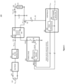
- Figure 1 illustrates an isolated switched-mode power converter 100 making use of a two-level switch driver 160 that limits a voltage V DS_Q2 across a synchronous rectification (SR) switch Q2 during burst-mode operation.
- the power converter 100 includes an AC input 102, a DC input 104, an output 106, a rectifier 120, a power factor correction (PFC) circuit 130, a transformer 140, a power stage 150, and a controller 190.
- PFC power factor correction
- the AC input 102 is for connecting to an AC power supply 110, which supplies an AC voltage V AC_IN .
- the AC power supply 110 is not part of the isolated power converter 100.
- the rectifier 120 rectifies the AC voltage V AC_IN , providing a DC voltage at its output.
- the optional power factor correction (PFC) and protection circuit may provide several functions, including correcting the power factor of the power converter by boosting the DC voltage provided by the rectifier 120, providing protection against voltage spikes or other input anomalies, and filtering the input voltage.
- the rectifier 120 and PFC 130 may be swapped in order, or may be integrated within a combined circuit.
- the PFC 130 outputs a DC voltage V DC_IN that is appropriate for coupling to the transformer 140.
- the illustrated power converter 100 provides AC-to-DC conversion, but a DC-to-DC variant may be realized by omitting the rectifier 120 and PFC 130, and coupling the DC input 104 to a DC power supply, e.g., a battery or another power converter that provides DC power.
- a DC power supply e.g., a battery or another power converter that provides DC power.
- the transformer 140 includes a primary winding 142 having N1 turns, a secondary winding 144 having N2 turns, and a core 146.
- the transformer provides a voltage step-down (or step-up) according to the turns ratio N1 :N2.
- the secondary side of the isolated power converter 100 includes an output capacitor Co, the SR switch Q2, and the output 106.
- the output capacitor Co filters the voltage pulses provided by the secondary winding 144 and the SR switch Q2, thereby providing a relatively constant voltage V OUT at the output 106.
- the output 106 is for connecting to a load 170, which is not actually part of the power converter 100.
- the SR switch Q2 switchably connects one side of the secondary winding 144 to ground, thereby rectifying the voltage V OUT provided at the output.
- the SR switch Q2 illustrated in Figure 1 is an enhancement-mode metal-oxide-semiconductor field-effect transistor (MOSFET), but other switch types may be used.
- MOSFET metal-oxide-semiconductor field-effect transistor
- JFETs junction field-effect transistors
- BJTs bipolar junction transistors
- IGBTs insulated gate bipolar transistors
- HEMTs high electron mobility transistors
- GaN Gallium Nitride MOSFETs
- power transistors may be preferred in some applications.
- transistor types have a maximum allowed voltage, such as an avalanche breakdown voltage.
- the controller 190 and its constituent parts may be implemented using a combination of analog hardware components (such as transistors, amplifiers, diodes, and resistors), and processor circuitry that includes primarily digital components.
- the processor circuitry may include one or more of a digital signal processor (DSP), a general-purpose processor, and an application-specific integrated circuit (ASIC).
- DSP digital signal processor
- ASIC application-specific integrated circuit
- the controller 190 may also include memory, e.g., non-volatile memory such as flash, which includes instructions or data for use by the processor circuitry, and one or more timers.
- the controller 190 inputs sensor signals such as signals corresponding to the output voltage V OUT and a sensed output current I OUT_SENSE .
- the controller 190 is responsible for controlling the power converter 100 so as to supply necessary power to the load 170.
- the controller 190 senses the output voltage V OUT and current I OUT_SENSE , and uses these measurements to generate control signals CTL_Q1, CTL_Q2 for controlling the primary-side power stage 150 and the secondary-side SR switch Q2.
- a rectifier controller within the controller 190 generates the control signal CTL_Q2 based upon a sensed current through the SR switch Q2, sensed secondary-side voltages such as the drain-to-source voltage V DS_Q2 , or timing from a pulse-width-modulation (PWM) generator 192.
- PWM pulse-width-modulation
- the control signal CTL_Q2 is provided to a gate of the SR switch Q2, via a driver 180, thereby controlling conduction of the SR switch Q2.
- the controller 190 includes the PWM generator 192 and a low-power detector 194.
- the PWM generator 192 typically includes a linear feedback controller, such as a proportional-integral-derivative (PID) controller, for regulating the output voltage V OUT .
- PID proportional-integral-derivative
- the PWM generator 192 senses the output voltage V OUT and compares this voltage against a reference (target) voltage V TARGET to determine control parameters for generating the control signal CTL_Q1 for the power stage 150.
- the PWM generator 192 might generate control signals CTL_Q1 having a fixed switching frequency and variable duty cycle, in which case the determined control parameter is a duty cycle.
- the PWM generator 192 might generate control signals having fixed pulse widths and variable frequencies, in which case the control parameter is a switching frequency.
- the low-power detector 194 determines whether the power converter 100 should operate in a normal or a burst mode.
- the low-power detector 194 may detect that the load 170 is inactive by comparing the sensed current I OUT_SENSE against a low-power current threshold.
- the output current I OUT_SENSE may be sensed using a shunt resistor, a current transformer, the DC resistance (DCR) of an inductance associated with the secondary winding 144, or other current-sensing techniques. Because such current-sensing techniques are well known in the art, they are not described in further detail herein.
- a primary-side current flowing through the primary winding 142 and the power switch Q1 may be measured and used to sense that the load 170 is inactive. Sensing of a primary-side current may be preferred in some applications including, e.g., when a controller is located on the primary side rather than the secondary side of the power converter 190 and/or when current-mode control is used for the power switch Q1.
- Sensing of a primary-side current may use similar techniques as described previously for measuring the output current I OUT_SENSE , e.g., measuring the voltage across a shunt resistor connecting the source of the power transistor Q2 to ground, measuring the drain-to-source voltage of the power transistor Q2, etc.
- sensing of the output current I OUT_SENSE via measurement of a primary-side current is not shown in Figure 1 .
- the low-power detector 194 indicates, via a burst-mode indicator BRST, that the power converter 100 should enter a burst mode of operation responsive to detecting that the load 170 is inactive, e.g., in a low-power state. Such inactivity may be determined, e.g., by detecting that the output current I OUT_SENSE is below the low-power current threshold or, similarly, that a primary-side current is below a corresponding primary-side low-power current threshold. While in burst-mode operation, the PWM generator 192 ceases generation of control signals CTL_Q1 for the power stage 150 for large intervals of time.
- the net effect is that the PWM generator 192, during burst-mode operation, provides bursts of pulses on the control signal CTL_Q1, separated by long intervals of inactivity.
- the controller 190 may be located on the primary or secondary side of the power converter 100. So as to maintain the integrity of the primary-to-secondary boundary, signals input or output from the controller 190 may need to pass through isolators, which are not shown for ease of illustration. For example, a controller 190 located on the secondary side would require that the output signals CTL_Q1, BRST provided to the (primary-side) power stage 150 be passed through isolators. Conversely, a primary-side controller would require that the other input and output signals to the controller 190 be passed through isolators.
- the power stage 150 includes a power switch Q1 and a two-level switch driver 160.
- the power switch Q1 switchably connects one terminal, corresponding to the illustrated node VSW, of the primary winding 142 to ground, thereby generating voltage pulses across the primary winding 142.
- the illustrated power switch Q1 is a MOSFET having gate, drain and source terminals. In some applications, other switch types may be preferred such as junction field-effect transistors (JFETs), bipolar junction transistors (BJTs), insulated gate bipolar transistors (IGBTs), Gallium Nitride (GaN) MOSFETs or high electron mobility transistors (HEMTs).
- JFETs junction field-effect transistors
- BJTs bipolar junction transistors
- IGBTs insulated gate bipolar transistors
- GaN Gallium Nitride
- HEMTs high electron mobility transistors
- the gate of the power switch Q1 is charged at different rates by the two-level switch driver 160, according to the burst-mode indication BRST input to the power stage 150.
- the switch driver 160 disables at least some of its sourcing current, so that the gate of the power switch Q1 is charged more slowly.
- FIG. 2 illustrates a particular embodiment for a power stage 250, including a two-level switch driver 260, in further detail.
- the switch driver 260 provides a gate signal GS_Q1 to the gate (G) of the power switch Q1, by sourcing or sinking current to the gate via a push-pull arrangement of driver switches.
- the switch driver 260 includes pull-up driver switches MPa, MPb and a pull-down driver switch MN1.
- Pre-drivers 264, 266, 268 provide gate signals GHa, GHb, GL for each of the driver switches MPa, MPb, MN1.
- the pull-down driver switch MN1 is an n-channel MOSFET, meaning that this switch is set to conduct when a high voltage is provided to its gate.
- the pull-up driver switches MPa, MPb are p-channel MOSFETs, meaning that they are set to conduct when a low voltage, e.g., 0V, is provided to their respective gates.
- the first pull-up driver switch MPa has a low on-state resistance R DS_ON
- the second pull-up driver switch MPb has a high on-state resistance.
- the first pull-up driver switch MPa is controlled by a gate signal GHa output from a high-side control circuit 262.
- the high-side control circuit 262 effectively disables the first pull-up driver switch MPa when burst-mode operation is indicated.
- the high-side control circuit 262 includes an OR gate 263 and a first high-side pre-driver 264. During normal operation, the burst-mode indication BRST is low and the OR gate 263 passes the control signal CTL_Q2 through to the first high-side pre-driver 264. In this state, the first and second pull-up driver switches are switched simultaneously according to the control signal CTL_Q2.
- a high voltage (VDD) for the control signal CTL_Q2 is passed through to the gate terminals of the pull-up driver switches MPa, MPb, such that their gate-to-source voltages V GS_MPa , V GS_MPb are zero and the switches are turned off.
- a low voltage (0V) for the control signal CTL_Q2 is passed through to the gate terminals of the pull-up driver switches MPa, MPb, such that their gate-to-source voltages V GS_MPa , V GS_MPb are (-VDD) and the switches are turned on.
- the burst-mode indication BRST is high and the output of the OR gate 263 stays high regardless of the state of the control signal CTRL_Q2.
- the second pull-up driver switch MPb is controlled by the control signal CTRL_Q2, and has no dependence on the burst-mode indication BRST.
- the low-side driver switch MN1 is turned on when the control signal CTL_Q2 is high (logical "1"), and turns off when this signal is low (0V). When turned on, the low-side driver switch MN1 sinks current from the gate of the power switch Q1, thereby turning the power switch Q1 off.
- the current-sourcing ability of the pull-up driver stage is determined by its on-state resistance. During burst mode, only the second (high resistance) pull-up driver switch is enabled, meaning that the current sourcing ability is considerably reduced relative to normal operation. With a lower sourcing current provided to the gate of the power switch Q1, the power switch Q1 turns on more slowly and the voltage pulse generated across the primary winding 142 has a low slew rate.
- the on-state resistance of a switch is typically determined by its size, e.g., channel length and width.
- the channel widths of the first and second pull-up driver switches MPa, MPb may be set to achieve a desired ratio of the on-state resistances or, similarly, an absolute desired on-state resistance of the second pull-up driver switch MPb that leads to a desired voltage slew rate across a secondary-side SR switch such as Q2 in Figure 1 .
- the pull-up driver switches MPa, MPb may be portions of the same device, but have separate control terminals.
- a MOSFET may have multiple source and drain regions connected in parallel, wherein a gate finger is provided to control each source/drain region. Multiple gate fingers may be tied together, to effectively create a larger MOSFET having lower on-state resistance than a single source/drain portion of the MOSFET.
- the gate fingers may be partitioned into one group allocated to the first pull-up driver switch MPa, and another group allocated to the second pull-up driver switch MPb.
- a MOSFET having 120 gate fingers may be characterized in that each drain/source pair may has an effective on-state resistance of 600 Q.
- One such finger may be allocated to control one drain/source pair making up the second (high-resistance) pull-up driver switch MPb.
- the remaining 119 fingers may be allocated to control the remaining 119 drain/source pairs which make up the first (low-resistance) pull-up driver switch MPa.
- the allocation of gate fingers between the first and second pull-up driver switches MPa may be done during fabrication via a metal mask, or be otherwise programmable, e.g., using a digital code to allocate MOSFET sections between the first and second pull-up driver switches.
- the pre-drivers 264, 266 for the first and second pull-up driver switches MPa, MPb must be sized according to the size of the pull-up driver switches MPa, MPb, e.g., the number of sections allocated.
- the overall pull-up driver strength characterized by the combined on resistance of the pull-up driver switches MPa, MPb in parallel, must be sized to provide the source current required by the gate of the power switch Q1 during normal operation of the power converter 100.
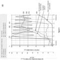
- Figure 3 illustrates waveforms 300 corresponding to the drain-to-source voltage V DS_Q2 across the SR switch Q2 for different power converter circuits.
- These waveforms 300 are initiated by voltage pulses applied across a primary-side winding using a primary-side power switch such as Q1 within Figure 1 , wherein the voltage pulses induce secondary-side voltage pulses leading to the drain-to-source voltage waveforms 300 illustrated.
- These waveforms are generated during a low-power (standby) mode, during which there is negligible current drawn by a load of the respective power converters.
- a first waveform 310 corresponds to a first power converter in which no mitigation is provided for the steep rising edge of the voltage pulse.
- the voltage attempts to ring to a high voltage, but the SR switch clamps 312 the voltage at an avalanche breakdown voltage of approximately 165V.
- the SR switch conducts excessive current levels and the SR switch is potentially damaged, particularly when the avalanche breakdown occurs repetitively.
- a second waveform 320 corresponds to a second power converter in which a snubber circuit, such as the RCD snubber described previously, limits the maximum voltage across the SR switch.
- the peak voltage of this second waveform only reaches about 158 V, meaning that avalanche breakdown of the SR switch is avoided.
- the third waveform 330 corresponds to a third power converter, which includes a two-level switch driver as illustrated in Figure 2 .
- the drain-to-source voltage of the SR switch rises more slowly than either the first or the second waveforms 310, 320.
- Avalanche breakdown of the SR switch is avoided, without the necessity of an RCD circuit and its components.
- the maximum voltage of approximately 125V across the SR switch is significantly lower than in the power converters having no protection or having an RCD snubber.
- FIG 4 illustrates waveforms 400 corresponding to energy consumed from an input power source for the power converter circuits described in relation to Figure 3 .
- the first energy waveform 410 corresponds to the consumed energy for the first power converter, in which no mitigation for the steep rising voltage pulse is provided.
- the second energy waveform 420 corresponds to the energy consumed for the second power converter, in which a snubber circuit is used to avoid avalanche breakdown in the SR switch. Note that more energy is consumed for this power converter, due to the energy consumption of the snubber.
- the third energy waveform 430 corresponds to the energy consumed for the third power converter, in which a two-level switch driver, such as the switch driver 260 of Figure 2 , is used for switching a primary-side power stage. It can be seen that the energy consumption incurred by the third power converter, making use of a two-level switch driver, is much lower than the other illustrated alternatives.
- Figure 5 illustrates a method 500 for controlling a primary-side power switch within an isolated power converter, so as to prevent excessive voltage levels across a secondary-side SR switch.
- the method 500 may be implemented within an isolated power converter, such as the one illustrated in Figure 1 .
- the method 500 begins by sensing 510 the power P LOAD drawn by a load of the power converter, and comparing 520 this power P LOAD against a low-power threshold P LP_THRESH .
- a load current e.g., I OUT_SENSE in Figure 1
- a low-power current threshold I LP_THRESH may be sensed and compared against a low-power current threshold I LP_THRESH .
- the power converter enters 530 a burst mode of operation, and a first (low-resistance) pull-up driver switch is disabled.
- the burst-mode operation continues until the power P LOAD drawn by the load exceeds the low-power threshold P LP_THRESH , as indicated by sensing 550 the drawn power P LOAD .
- burst-mode operation is exited 570 and normal operation resumes.
- the first (low-resistance) pull-up driver switch is enabled 580.
- a non-isolated buck-boost power converter uses an inductor to temporarily store energy rather than using a transformer to transfer energy across an isolation barrier.
- a power switch switch ably connects an input power source to the energy-storage inductor, thereby generating an AC voltage across the inductor.
- the AC voltage is rectified, e.g., using an SR switch, and the resultant DC voltage is provided to a load of the power converter.
- the SR switch in such a buck-boost converter may be subject to excessive voltages, including an avalanche breakdown voltage limit, during periods when the load is inactive and not drawing significant current.
- the two-level switch driver described previously and illustrated in Figure 2 may be similarly used in such a non-isolated buck-boost power converter. More particularly, the two-level switch driver may drive the power switch that couples the input power source to the energy storage inductor. During periods when the load is drawing low power and particularly when such a state causes burst-mode operation, the two-level driver is placed in a state where only its high-resistance pull-up driver is enabled, as described previously.
- a burst-mode indication e.g., the BRST signal in Figure 2
- the voltage pulses provided to the energy-storage inductor have lower rising edges, and the extent of any voltage ringing across the SR switch is thereby reduced.
- the switch driver is configured to control a power switch located in a switched-mode power converter, so as to prevent excessive voltage levels across a synchronous rectification (SR) switch of the power converter.
- the switch driver comprises a pull-down driver switch, two pull-up driver switches, a mode indication input, a switch control input, and a high-side control circuit.
- the pull-down driver switch sinks current from a control terminal of the power switch.
- the pull-up driver switches source current to the control terminal.
- a first of the pull-up switches has a first on-state resistance, and a second has a second on-state resistance, wherein the second on-state resistance is substantially higher than the first on-state resistance.
- the mode indication input indicates whether the power converter is operating in a burst mode or not.
- the switch control input controls the conductivity of the pull-down driver switch, the second (high resistance) pull-up driver switch and, in conjunction with the mode indication input, the first pull-up driver switch.
- the high-side control circuit disables the first (low resistance) pull-up driver switch when burst-mode operation is indicated at the mode indication input.
- the pull-down driver switch is an n-channel metal-oxide semiconductor field-effect transistor (MOSFET), and the first and second pull-up driver switches are p-channel MOSFETs.
- MOSFET metal-oxide semiconductor field-effect transistor
- the high-side control circuit comprises a high-side pre-driver and an inclusive OR gate.
- the high-side pre-driver is coupled to and controls conductivity of the first pull-up driver switch.
- the inclusive OR gate inputs the mode indication and the switch control signal, and outputs a high-side switch control signal to the high-side pre-driver.
- the second pull-up driver switch is sized so as to source a current level that limits the voltage levels across the SR switch to be lower than an upper voltage limit of the SR switch, the upper voltage limit corresponding to an avalanche breakdown voltage of the SR switch.
- the first pull-up driver switch when turned on, sources a current level at least 100 times a current level sourced by the second pull-up driver switch, when the second pull-up driver switch is turned on.
- a size ratio between the first and second pull-up driver switches is programmable by a configurable digital code.
- a size ratio between the first and second pull-up driver switches is set by a metal option during fabrication of the pull-up driver switches.
- the method is for controlling a power switch of the power converter so as to prevent excessive voltage levels across a synchronous rectification (SR) switch of the power converter.
- the power converter includes a switch driver configured as described above including, notably, first and second pull-up driver switches.
- the method comprises detecting that a load of the power converter is drawing power below a low-power threshold, e.g., that the load is in a standby mode. Responsive to such detecting, a burst mode of operation is entered and the first pull-up driver switch is disabled.
- the SR switch has an associated avalanche breakdown voltage corresponding to a voltage limit across first and second terminals of the SR switch, and the on-state resistance of the second pull-up driver switch is configured to support a current level through the second pull-up driver switch such that a rate at which the power switch turns on ensures that the voltage across the first and second terminals of the SR switch stays below the avalanche breakdown voltage of the SR switch.
- the method also comprises exiting the burst mode of operation and enabling the first pull-up driver switch, responsive to detecting that the load of the power converter is drawing more than the low power level.
- the isolated power converter comprises an input, an output, a transformer, a power stage, an SR switch, and a controller.
- the input is for coupling to an input power source, whereas the output is for coupling to a load of the power converter.
- the transformer includes primary and secondary windings.
- the power stage is configured to switch power from the input to the primary winding.
- the power stage includes a power switch and a switch driver for controlling the power switch.
- the switch driver is configured as described above and, notably, includes first and second pull-up driver switches, wherein the first pull-up driver switch is disabled responsive to the power converter entering a burst mode of operation (standby).
- the SR switch is configured to rectify power provided by the secondary winding such that DC power is provided to the output, and has an SR voltage across its terminals.
- the SR switch has an avalanche breakdown voltage level associated with the SR voltage.
- the controller is configured to control the power transferred to the output by generating a switch control signal to drive the power stage.
- the controller also generates, responsive to detecting a low-power state, a burst-mode indication, which is used to disable the first pull-up driver switch.
- the low-power state is detected based upon a sensed current and/or a sensed voltage of the load.
- the pull-down driver switch is an n-channel metal-oxide semiconductor field-effect transistor (MOSFET), and the first and second pull-up driver switches are p-channel MOSFETs.
- MOSFET metal-oxide semiconductor field-effect transistor
- the high-side control circuit comprises a high-side pre-driver and an inclusive OR gate.
- the high-side pre-driver is coupled to and controls conductivity of the first pull-up driver switch.
- the inclusive OR gate inputs the mode indication and the switch control signal, and outputs a high-side switch control signal to the high-side pre-driver.
- the second pull-up driver switch is sized so as to source a current level that limits the voltage levels across the SR switch of the secondary side to be lower than an upper voltage limit of the SR switch, the upper voltage limit corresponding to an avalanche breakdown voltage of the SR switch.
- the first pull-up driver switch when turned on, sources a current level at least 100 times a current level sourced by the second pull-up driver switch, when the second pull-up driver switch is turned on.
- a size ratio between the first and second pull-up driver switches is programmable by a configurable digital code.
- a size ratio between the first and second pull-up driver switches is set by a metal option during fabrication of the pull-up driver switches.
- the isolated power converter has a flyback converter topology.
Landscapes
- Engineering & Computer Science (AREA)
- Power Engineering (AREA)
- Dc-Dc Converters (AREA)
Claims (15)
- Circuit d'attaque de commutateur configuré pour commander un commutateur (Q1) de puissance dans un convertisseur de puissance en mode commuté, de manière à prévenir des niveaux de tension excessifs aux bornes d'un commutateur (Q2) synchrone de redressement (SR) du convertisseur de puissance, le circuit d'attaque (160 ; 260) de commutateur comprenant :un commutateur(MN1) de circuit d'attaque pull-down pour abaisser du courant provenant d'une borne (GS_Q1) de commande du commutateur (Q1) de puissance ;un premier commutateur (MPa) de circuit d'attaque pull-up pour fournir du courant à la borne (GS_Q1) de commande, le premier commutateur (MPa) de circuit d'attaque pull-up ayant une première résistance à l'état de conduction ;un deuxième commutateur (MPb) de circuit d'attaque pull-up pour fournir du courant à la borne (GS_Q1) de commande, le deuxième commutateur (MPb) de circuit d'attaque pull-up ayant une deuxième résistance à l'état de conduction sensiblement plus grande que la première résistance à l'état de conduction ;une entrée d'indication de mode configurée pour recevoir une indication (BRST) de mode ;une entrée de commande de commutateur configurée pour recevoir un signal (CTL_Q1) de commande, qui commande le commutateur (MN1) de circuit d'attaque pull-down, le premier commutateur (MPa) de circuit d'attaque pull-up et le deuxième commutateur (MPb) de circuit d'attaque pull-up ; etun circuit (262) de commande de côté haut configuré pour mettre hors circuit le premier commutateur (MPa) de circuit d'attaque pull-up en réaction à une indication en mode rafale à l'entrée de l'indication de mode.
- Circuit d'attaque de commutateur suivant la revendication 1, dans laquelle le commutateur (MN1) de circuit d'attaque pull-down est un transistor à effet de champ métal oxyde semiconducteur (MOSFET) à canal n et le premier et le deuxième commutateurs (MPa, MPb) de circuit d'attaque pull-up sont des MOSFET à canal p.
- Circuit d'attaque de commutateur suivant la revendication 1 ou 2, dans laquelle le circuit (262) de commande du côté haut comprend :un circuit de préattaque (264) de côté haut pour commander le premier commutateur (MPa) de circuit d'attaque pull-up ;une porte (263) OU inclusif ayant des entrées reliées à l'entrée d'indication de mode et à l'entrée de commande de commutateur et ayant une sortie reliée à une entrée du circuit de préattaque (264) de côté haut.
- Circuit d'attaque de commutateur suivant l'une quelconque des revendications 1 à 3, dans laquelle le deuxième commutateur (MPb) de circuit d'attaque pull-up est dimensionné de manière à fournir un niveau de courant, qui limite les niveaux de tension aux bornes du commutateur (Q2) SR, afin que la tension soit inférieure à une limite supérieure de tension du commutateur (Q2) SR, la limite supérieure de tension correspondant à une tension de claquage d'avalanche du commutateur (Q2) SR.
- Circuit d'attaque de commutateur suivant l'une quelconque des revendications 1 à 4, dans laquelle le premier commutateur (MPa) de circuit d'attaque pull-up, lorsqu'il est dans l'état de conduction, fournit un niveau de courant représentant au moins 100 fois un niveau de courant fourni par le deuxième commutateur (MPb) de circuit d'attaque pull-up, lorsque le deuxième commutateur (MPb) de circuit d'attaque pull-up est dans l'état de conduction.
- Circuit d'attaque de commutateur suivant l'une quelconque des revendications 1 à 5, dans laquelle un rapport de dimension entre le premier et le deuxième commutateurs (MPa, MPb) de circuit d'attaque pull-up est programmable par un code numérique configurable.
- Circuit d'attaque de commutateur suivant l'une quelconque des revendications 1 à 5, dans laquelle un rapport de dimension entre le premier et le deuxième commutateurs (MPa, MPb) de circuit d'attaque pull-up est fixé par une option métallique pendant la fabrication des commutateurs (MPa, MPb) de circuit d'attaque pull-up.
- Procédé de commande d'un commutateur (Q1) de puissance dans un convertisseur de puissance en mode commuté, de manière à prévenir des niveaux de tension excessifs aux bornes d'un commutateur (Q2) synchrone de redressement (SR) du convertisseur de puissance, le convertisseur de puissance comprenant une Circuit d'attaque (160 ; 260) de commutateur comprenant un premier et un deuxième commutateurs (MPa, MPb) de circuit d'attaque pull-up, dans lequel le deuxième commutateur (MPb) de circuit d'attaque pull-up a une résistance à l'état de conduction sensiblement plus grande qu'une résistance à l'état de conduction du premier commutateur (MPa) de circuit d'attaque pull-up, le procédé comprenant :détecter qu'une charge du convertisseur de puissance tire un niveau bas de puissance ;en réaction à la détection, entrer dans un mode rafale de fonctionnement et invalider le premier commutateur (MPa) de circuit d'attaque pull-up.
- Procédé suivant la revendication 8,
dans lequel le commutateur (Q2) SR a une tension de claquage d'avalanche associée correspondant à une limite de tension aux bornes des première et deuxième bornes du commutateur (Q2) SR, et dans lequel la résistance à l'état de conduction du deuxième commutateur (MPb) de circuit d'attaque pull-up est configurée pour supporter un niveau de courant dans le deuxième commutateur (MPb) de circuit d'attaque pull-up, de manière à ce qu'une vitesse, à laquelle le commutateur (Q1) de puissance passe à l'état de conduction, assure que la tension aux bornes des première et deuxième bornes du commutateur (Q2) SR reste en dessous de la tension de claquage d'avalanche du commutateur (Q2) SR. - Procédé suivant la revendication 8 ou 9, comprenant :
en réaction de la détection que la charge du convertisseur tire plus que le niveau bas de puissance, sortir du mode de fonctionnement en rafale et valider le premier interrupteur (MPa) de circuit d'attaque pull-up. - Convertisseur de puissance isolé, comprenant :une entrée de liaison à une source (110) d'entrée de puissance ;une sortie (106) de liaison et une charge ;un transformateur (140) comprenant un enroulement (142) primaire et un enroulement (144) secondaire ;un étage (150) de puissance configuré pour commuter de la puissance de l'entrée à l'enroulement (142) primaire, l'étage (150) de puissance comprenant un commutateur (Q1) de puissance et une Circuit d'attaque (160 ; 260) de commutateur conformément à la revendication 1 pour commander le commutateur (Q1) de puissance ;un commutateur (Q2) synchrone de redressement (SR) configuré pour redresser de la puissance fournie par l'enroulement (144) secondaire, le commutateur (Q2) SR ayant une tension (VDS_Q2) SR aux bornes des première et deuxième bornes du commutateur (Q2) SR ayant un niveau de tension de claquage d'avalanche associée à la tension (VDS_Q2) SR ; etune unité (190) de commande configurée pour commander un transfert de puissance à la sortie en créant un signal (CTL_Q1) de commande de commutateur, et pour créer une indication (BRST) de mode rafale, après détection que la charge est dans un état de puissance faible.
- Convertisseur de puissance isolé suivant la revendication 11, dans lequel le commutateur (MN1) de circuit d'attaque pull-down est un transistor à effet de champ métal oxyde semiconducteur (MOSFET) à canal n et le premier et le deuxième commutateurs (MPa, MPb) de circuit d'attaque pull-up sont des MOSFET à canal p.
- Convertisseur de puissance isolé suivant la revendication 12, dans lequelle circuit de commande de côté haut comprend un premier circuit de préattaque (264) de côté haut pour commander le premier commutateur (MPa) de circuit d'attaque pull-up ;une porte (263) OU inclusif ayant des entrées configurées pour recevoir l'indication (BRST) de mode rafale et le signal (CTL_Q1) de commande et ayant une sortie reliée à une entrée de du circuit de préattaque (264) de côté haut.
- Convertisseur de puissance isolé suivant l'une quelconque des revendications 1 à 13, dans lequel le deuxième commutateur (MPb) de circuit d'attaque pull-up est dimensionné de manière à fournir un niveau de courant, qui limite le niveau de tension aux bornes des première et deuxième bornes du commutateur (Q2) SR, de manière à ce qu'il soit inférieur à une limite supérieure de tension du commutateur (Q2) SR, la limite supérieure de tension correspondant à la tension de claquage d'avalanche du commutateur (Q2) SR.
- Convertisseur de puissance isolé suivant l'une quelconque des revendications 11 à 14, dans lequel le convertisseur de puissance isolé a une topologie de convertisseur indirect.
Applications Claiming Priority (1)
| Application Number | Priority Date | Filing Date | Title |
|---|---|---|---|
| US16/209,102 US10707767B2 (en) | 2018-12-04 | 2018-12-04 | Two-level switch driver for preventing avalanche breakdown for a synchronous rectification switch in a power converter operating in a low-power burst mode |
Publications (2)
| Publication Number | Publication Date |
|---|---|
| EP3664295A1 EP3664295A1 (fr) | 2020-06-10 |
| EP3664295B1 true EP3664295B1 (fr) | 2024-02-21 |
Family
ID=68762569
Family Applications (1)
| Application Number | Title | Priority Date | Filing Date |
|---|---|---|---|
| EP19212827.0A Active EP3664295B1 (fr) | 2018-12-04 | 2019-12-02 | Commande de commutateur à deux niveaux pour empêcher un effet d'avalanche pour un commutateur de redressement synchrone dans un convertisseur de puissance fonctionnant en mode rafale à faible puissance |
Country Status (3)
| Country | Link |
|---|---|
| US (1) | US10707767B2 (fr) |
| EP (1) | EP3664295B1 (fr) |
| CN (1) | CN111277119B (fr) |
Families Citing this family (14)
| Publication number | Priority date | Publication date | Assignee | Title |
|---|---|---|---|---|
| CN111564971B (zh) * | 2019-08-21 | 2025-09-16 | 杰华特微电子股份有限公司 | 开关电源电路的控制方法、控制电路及开关电源电路 |
| US11031922B1 (en) * | 2019-12-03 | 2021-06-08 | Alpha And Omega Semiconductor (Cayman) Limited | Switch circuit with reduced switch node ringing |
| US11031929B1 (en) * | 2020-07-30 | 2021-06-08 | Infineon Technologies Ag | Actively tracking switching speed control of a power transistor |
| US12068696B2 (en) * | 2020-09-22 | 2024-08-20 | Semiconductor Components Industries, Llc | Methods and systems related to operation of a switching power converter |
| CN113037069B (zh) * | 2021-03-12 | 2022-07-15 | 杰华特微电子股份有限公司 | 一种开关保护电路和功率变换器 |
| EP4423893A1 (fr) * | 2021-10-26 | 2024-09-04 | Telefonaktiebolaget LM Ericsson (publ) | Alimentation électrique et procédé mis en oeuvre par une alimentation électrique |
| CN118216089A (zh) * | 2021-12-06 | 2024-06-18 | 罗姆股份有限公司 | 信号传递装置、电子设备、车辆 |
| CN115514239A (zh) * | 2022-01-28 | 2022-12-23 | 英诺赛科(苏州)半导体有限公司 | 开关模式电力供应、电子装置充电器及ac到dc转换器 |
| US11804783B2 (en) | 2022-02-01 | 2023-10-31 | Silanna Asia Pte Ltd | Dynamic intra-pulse-sequence switch transition-time controller |
| US12027978B2 (en) | 2022-05-31 | 2024-07-02 | Texas Instruments Incorporated | Switching regulator with configurable snubber |
| JP2024003305A (ja) * | 2022-06-27 | 2024-01-15 | ローム株式会社 | スイッチ駆動回路、電源制御装置、スイッチング電源 |
| IT202200019947A1 (it) * | 2022-09-28 | 2024-03-28 | St Microelectronics Srl | Procedimento per rilevare una corrente che fluisce in un transistore che pilota un carico, e corrispondente disposizione circuitale per il rilevamento |
| US12261605B2 (en) * | 2023-01-13 | 2025-03-25 | GM Global Technology Operations LLC | Gate driving with phased slew rate control and overcurrent protection |
| CN116360540B (zh) * | 2023-05-19 | 2023-09-29 | 四川奥库科技有限公司 | 用于芯片测试的电压调节系统及电压调节方法 |
Family Cites Families (10)
| Publication number | Priority date | Publication date | Assignee | Title |
|---|---|---|---|---|
| CN101841247B (zh) * | 2009-11-20 | 2013-01-23 | Bcd半导体制造有限公司 | 一种开关电源的基极驱动电路 |
| JP5928506B2 (ja) | 2014-02-28 | 2016-06-01 | サンケン電気株式会社 | スイッチング電源装置 |
| US20150280576A1 (en) * | 2014-03-26 | 2015-10-01 | Infineon Technologies Austria Ag | System and Method for a Switched Mode Power Supply |
| JP2016027775A (ja) | 2014-06-27 | 2016-02-18 | サンケン電気株式会社 | スイッチング電源装置 |
| EP3219010B1 (fr) * | 2014-11-11 | 2020-07-08 | Maschinenfabrik Reinhausen GmbH | Émulation de résistance et amplificateur de grille |
| US9627987B2 (en) | 2014-12-13 | 2017-04-18 | Richtek Technology Corporation | Flyback converter operating by synchronous rectification with transient protection, primary side control circuit therein, and control method thereof |
| TWI599160B (zh) * | 2015-05-06 | 2017-09-11 | 立錡科技股份有限公司 | 返馳式電源供應器及其控制器與驅動器 |
| US9742289B2 (en) * | 2015-06-23 | 2017-08-22 | Sanken Electric Co., Ltd. | Integrated circuit and switching power-supply device |
| US9825546B2 (en) * | 2016-03-30 | 2017-11-21 | Infineon Technologies Austria Ag | Circuits and methods for auxiliary secondary supply generation with self-starting primary side driver in isolated power converters |
| US10965281B2 (en) * | 2017-09-25 | 2021-03-30 | Dialog Semiconductor (Uk) Limited | Circuit based on a III/V semiconductor and a method of operating the same |
-
2018
- 2018-12-04 US US16/209,102 patent/US10707767B2/en active Active
-
2019
- 2019-12-02 EP EP19212827.0A patent/EP3664295B1/fr active Active
- 2019-12-03 CN CN201911219381.1A patent/CN111277119B/zh active Active
Also Published As
| Publication number | Publication date |
|---|---|
| CN111277119B (zh) | 2025-01-10 |
| CN111277119A (zh) | 2020-06-12 |
| US20200177090A1 (en) | 2020-06-04 |
| US10707767B2 (en) | 2020-07-07 |
| EP3664295A1 (fr) | 2020-06-10 |
Similar Documents
| Publication | Publication Date | Title |
|---|---|---|
| EP3664295B1 (fr) | Commande de commutateur à deux niveaux pour empêcher un effet d'avalanche pour un commutateur de redressement synchrone dans un convertisseur de puissance fonctionnant en mode rafale à faible puissance | |
| US8755203B2 (en) | Valley-mode switching schemes for switching power converters | |
| US9991800B2 (en) | Switched mode power supply with efficient operation at light loads and method therefor | |
| EP2621069B1 (fr) | Convertisseur à transfer indirect avec détection de tension primaire et protection à maximum de tension pendant l'opération avec charge faible | |
| US7570497B2 (en) | Discontinuous quasi-resonant forward converter | |
| US7738266B2 (en) | Forward power converter controllers | |
| US10855183B1 (en) | Method and device to operate a power switch in multiple modes | |
| US9647562B2 (en) | Power conversion with switch turn-off delay time compensation | |
| CN106537744B (zh) | 同步整流 | |
| US11451152B2 (en) | Active clamp circuit with steering network | |
| US10432097B2 (en) | Selection control for transformer winding input in a power converter | |
| US10461644B1 (en) | Synchronous rectification switch control with automatic compensation and reset | |
| WO2015065592A1 (fr) | Commande adaptative de redresseur synchrone | |
| GB2451088A (en) | Regulating the output of a forward power converter | |
| US11979090B2 (en) | Power converter controller with branch switch | |
| EP3977610B1 (fr) | Contrôle du fonctionnement d'un convertisseur de tension basé sur le courant inducteur | |
| US20170302176A1 (en) | System and Method for a Switched-Mode Power Supply | |
| US20240186903A1 (en) | Power converter controller with bias drive circuit for bias supply | |
| JP2003299354A (ja) | フライバックコンバータの同期整流回路 | |
| US9112353B2 (en) | Power supply device | |
| US20240154535A1 (en) | Switch mode power converter with synchronous rectifier implementing adaptive turn-off voltage | |
| KR101047339B1 (ko) | 전류 모드 제어기에서의 전류 검출 시스템 | |
| US20240204678A1 (en) | Enable circuit with winding signal detection | |
| TWI677177B (zh) | 電源控制裝置、及絕緣型開關電源裝置 | |
| TW202420722A (zh) | 具有實現自適應關斷電壓的同步整流器的開關模式功率轉換器及其方法 |
Legal Events
| Date | Code | Title | Description |
|---|---|---|---|
| PUAI | Public reference made under article 153(3) epc to a published international application that has entered the european phase |
Free format text: ORIGINAL CODE: 0009012 |
|
| STAA | Information on the status of an ep patent application or granted ep patent |
Free format text: STATUS: THE APPLICATION HAS BEEN PUBLISHED |
|
| AK | Designated contracting states |
Kind code of ref document: A1 Designated state(s): AL AT BE BG CH CY CZ DE DK EE ES FI FR GB GR HR HU IE IS IT LI LT LU LV MC MK MT NL NO PL PT RO RS SE SI SK SM TR |
|
| AX | Request for extension of the european patent |
Extension state: BA ME |
|
| STAA | Information on the status of an ep patent application or granted ep patent |
Free format text: STATUS: REQUEST FOR EXAMINATION WAS MADE |
|
| 17P | Request for examination filed |
Effective date: 20201210 |
|
| RBV | Designated contracting states (corrected) |
Designated state(s): AL AT BE BG CH CY CZ DE DK EE ES FI FR GB GR HR HU IE IS IT LI LT LU LV MC MK MT NL NO PL PT RO RS SE SI SK SM TR |
|
| GRAP | Despatch of communication of intention to grant a patent |
Free format text: ORIGINAL CODE: EPIDOSNIGR1 |
|
| STAA | Information on the status of an ep patent application or granted ep patent |
Free format text: STATUS: GRANT OF PATENT IS INTENDED |
|
| RIC1 | Information provided on ipc code assigned before grant |
Ipc: H02M 1/00 20060101ALN20230530BHEP Ipc: H02M 3/335 20060101ALI20230530BHEP Ipc: H03K 17/0812 20060101ALI20230530BHEP Ipc: H03K 17/16 20060101AFI20230530BHEP |
|
| INTG | Intention to grant announced |
Effective date: 20230616 |
|
| P01 | Opt-out of the competence of the unified patent court (upc) registered |
Effective date: 20230818 |
|
| GRAS | Grant fee paid |
Free format text: ORIGINAL CODE: EPIDOSNIGR3 |
|
| GRAJ | Information related to disapproval of communication of intention to grant by the applicant or resumption of examination proceedings by the epo deleted |
Free format text: ORIGINAL CODE: EPIDOSDIGR1 |
|
| GRAL | Information related to payment of fee for publishing/printing deleted |
Free format text: ORIGINAL CODE: EPIDOSDIGR3 |
|
| STAA | Information on the status of an ep patent application or granted ep patent |
Free format text: STATUS: REQUEST FOR EXAMINATION WAS MADE |
|
| GRAP | Despatch of communication of intention to grant a patent |
Free format text: ORIGINAL CODE: EPIDOSNIGR1 |
|
| STAA | Information on the status of an ep patent application or granted ep patent |
Free format text: STATUS: GRANT OF PATENT IS INTENDED |
|
| INTC | Intention to grant announced (deleted) | ||
| RIC1 | Information provided on ipc code assigned before grant |
Ipc: H02M 1/00 20060101ALN20231101BHEP Ipc: H02M 3/335 20060101ALI20231101BHEP Ipc: H03K 17/0812 20060101ALI20231101BHEP Ipc: H03K 17/16 20060101AFI20231101BHEP |
|
| INTG | Intention to grant announced |
Effective date: 20231114 |
|
| GRAA | (expected) grant |
Free format text: ORIGINAL CODE: 0009210 |
|
| STAA | Information on the status of an ep patent application or granted ep patent |
Free format text: STATUS: THE PATENT HAS BEEN GRANTED |
|
| AK | Designated contracting states |
Kind code of ref document: B1 Designated state(s): AL AT BE BG CH CY CZ DE DK EE ES FI FR GB GR HR HU IE IS IT LI LT LU LV MC MK MT NL NO PL PT RO RS SE SI SK SM TR |
|
| REG | Reference to a national code |
Ref country code: GB Ref legal event code: FG4D |
|
| REG | Reference to a national code |
Ref country code: CH Ref legal event code: EP |
|
| REG | Reference to a national code |
Ref country code: DE Ref legal event code: R096 Ref document number: 602019046843 Country of ref document: DE |
|
| REG | Reference to a national code |
Ref country code: IE Ref legal event code: FG4D |
|
| REG | Reference to a national code |
Ref country code: LT Ref legal event code: MG9D |
|
| REG | Reference to a national code |
Ref country code: NL Ref legal event code: MP Effective date: 20240221 |
|
| PG25 | Lapsed in a contracting state [announced via postgrant information from national office to epo] |
Ref country code: IS Free format text: LAPSE BECAUSE OF FAILURE TO SUBMIT A TRANSLATION OF THE DESCRIPTION OR TO PAY THE FEE WITHIN THE PRESCRIBED TIME-LIMIT Effective date: 20240621 |
|
| PG25 | Lapsed in a contracting state [announced via postgrant information from national office to epo] |
Ref country code: LT Free format text: LAPSE BECAUSE OF FAILURE TO SUBMIT A TRANSLATION OF THE DESCRIPTION OR TO PAY THE FEE WITHIN THE PRESCRIBED TIME-LIMIT Effective date: 20240221 |
|
| PG25 | Lapsed in a contracting state [announced via postgrant information from national office to epo] |
Ref country code: GR Free format text: LAPSE BECAUSE OF FAILURE TO SUBMIT A TRANSLATION OF THE DESCRIPTION OR TO PAY THE FEE WITHIN THE PRESCRIBED TIME-LIMIT Effective date: 20240522 |
|
| REG | Reference to a national code |
Ref country code: AT Ref legal event code: MK05 Ref document number: 1659996 Country of ref document: AT Kind code of ref document: T Effective date: 20240221 |
|
| PG25 | Lapsed in a contracting state [announced via postgrant information from national office to epo] |
Ref country code: NL Free format text: LAPSE BECAUSE OF FAILURE TO SUBMIT A TRANSLATION OF THE DESCRIPTION OR TO PAY THE FEE WITHIN THE PRESCRIBED TIME-LIMIT Effective date: 20240221 Ref country code: RS Free format text: LAPSE BECAUSE OF FAILURE TO SUBMIT A TRANSLATION OF THE DESCRIPTION OR TO PAY THE FEE WITHIN THE PRESCRIBED TIME-LIMIT Effective date: 20240521 Ref country code: HR Free format text: LAPSE BECAUSE OF FAILURE TO SUBMIT A TRANSLATION OF THE DESCRIPTION OR TO PAY THE FEE WITHIN THE PRESCRIBED TIME-LIMIT Effective date: 20240221 |
|
| PG25 | Lapsed in a contracting state [announced via postgrant information from national office to epo] |
Ref country code: ES Free format text: LAPSE BECAUSE OF FAILURE TO SUBMIT A TRANSLATION OF THE DESCRIPTION OR TO PAY THE FEE WITHIN THE PRESCRIBED TIME-LIMIT Effective date: 20240221 |
|
| PG25 | Lapsed in a contracting state [announced via postgrant information from national office to epo] |
Ref country code: AT Free format text: LAPSE BECAUSE OF FAILURE TO SUBMIT A TRANSLATION OF THE DESCRIPTION OR TO PAY THE FEE WITHIN THE PRESCRIBED TIME-LIMIT Effective date: 20240221 |
|
| PG25 | Lapsed in a contracting state [announced via postgrant information from national office to epo] |
Ref country code: RS Free format text: LAPSE BECAUSE OF FAILURE TO SUBMIT A TRANSLATION OF THE DESCRIPTION OR TO PAY THE FEE WITHIN THE PRESCRIBED TIME-LIMIT Effective date: 20240521 Ref country code: NO Free format text: LAPSE BECAUSE OF FAILURE TO SUBMIT A TRANSLATION OF THE DESCRIPTION OR TO PAY THE FEE WITHIN THE PRESCRIBED TIME-LIMIT Effective date: 20240521 Ref country code: NL Free format text: LAPSE BECAUSE OF FAILURE TO SUBMIT A TRANSLATION OF THE DESCRIPTION OR TO PAY THE FEE WITHIN THE PRESCRIBED TIME-LIMIT Effective date: 20240221 Ref country code: LT Free format text: LAPSE BECAUSE OF FAILURE TO SUBMIT A TRANSLATION OF THE DESCRIPTION OR TO PAY THE FEE WITHIN THE PRESCRIBED TIME-LIMIT Effective date: 20240221 Ref country code: IS Free format text: LAPSE BECAUSE OF FAILURE TO SUBMIT A TRANSLATION OF THE DESCRIPTION OR TO PAY THE FEE WITHIN THE PRESCRIBED TIME-LIMIT Effective date: 20240621 Ref country code: HR Free format text: LAPSE BECAUSE OF FAILURE TO SUBMIT A TRANSLATION OF THE DESCRIPTION OR TO PAY THE FEE WITHIN THE PRESCRIBED TIME-LIMIT Effective date: 20240221 Ref country code: GR Free format text: LAPSE BECAUSE OF FAILURE TO SUBMIT A TRANSLATION OF THE DESCRIPTION OR TO PAY THE FEE WITHIN THE PRESCRIBED TIME-LIMIT Effective date: 20240522 Ref country code: FI Free format text: LAPSE BECAUSE OF FAILURE TO SUBMIT A TRANSLATION OF THE DESCRIPTION OR TO PAY THE FEE WITHIN THE PRESCRIBED TIME-LIMIT Effective date: 20240221 Ref country code: ES Free format text: LAPSE BECAUSE OF FAILURE TO SUBMIT A TRANSLATION OF THE DESCRIPTION OR TO PAY THE FEE WITHIN THE PRESCRIBED TIME-LIMIT Effective date: 20240221 Ref country code: BG Free format text: LAPSE BECAUSE OF FAILURE TO SUBMIT A TRANSLATION OF THE DESCRIPTION OR TO PAY THE FEE WITHIN THE PRESCRIBED TIME-LIMIT Effective date: 20240221 Ref country code: AT Free format text: LAPSE BECAUSE OF FAILURE TO SUBMIT A TRANSLATION OF THE DESCRIPTION OR TO PAY THE FEE WITHIN THE PRESCRIBED TIME-LIMIT Effective date: 20240221 |
|
| PG25 | Lapsed in a contracting state [announced via postgrant information from national office to epo] |
Ref country code: PL Free format text: LAPSE BECAUSE OF FAILURE TO SUBMIT A TRANSLATION OF THE DESCRIPTION OR TO PAY THE FEE WITHIN THE PRESCRIBED TIME-LIMIT Effective date: 20240221 Ref country code: PT Free format text: LAPSE BECAUSE OF FAILURE TO SUBMIT A TRANSLATION OF THE DESCRIPTION OR TO PAY THE FEE WITHIN THE PRESCRIBED TIME-LIMIT Effective date: 20240621 |
|
| PG25 | Lapsed in a contracting state [announced via postgrant information from national office to epo] |
Ref country code: SE Free format text: LAPSE BECAUSE OF FAILURE TO SUBMIT A TRANSLATION OF THE DESCRIPTION OR TO PAY THE FEE WITHIN THE PRESCRIBED TIME-LIMIT Effective date: 20240221 Ref country code: PT Free format text: LAPSE BECAUSE OF FAILURE TO SUBMIT A TRANSLATION OF THE DESCRIPTION OR TO PAY THE FEE WITHIN THE PRESCRIBED TIME-LIMIT Effective date: 20240621 Ref country code: PL Free format text: LAPSE BECAUSE OF FAILURE TO SUBMIT A TRANSLATION OF THE DESCRIPTION OR TO PAY THE FEE WITHIN THE PRESCRIBED TIME-LIMIT Effective date: 20240221 Ref country code: LV Free format text: LAPSE BECAUSE OF FAILURE TO SUBMIT A TRANSLATION OF THE DESCRIPTION OR TO PAY THE FEE WITHIN THE PRESCRIBED TIME-LIMIT Effective date: 20240221 |
|
| PG25 | Lapsed in a contracting state [announced via postgrant information from national office to epo] |
Ref country code: DK Free format text: LAPSE BECAUSE OF FAILURE TO SUBMIT A TRANSLATION OF THE DESCRIPTION OR TO PAY THE FEE WITHIN THE PRESCRIBED TIME-LIMIT Effective date: 20240221 |
|
| PG25 | Lapsed in a contracting state [announced via postgrant information from national office to epo] |
Ref country code: SM Free format text: LAPSE BECAUSE OF FAILURE TO SUBMIT A TRANSLATION OF THE DESCRIPTION OR TO PAY THE FEE WITHIN THE PRESCRIBED TIME-LIMIT Effective date: 20240221 |
|
| PG25 | Lapsed in a contracting state [announced via postgrant information from national office to epo] |
Ref country code: CZ Free format text: LAPSE BECAUSE OF FAILURE TO SUBMIT A TRANSLATION OF THE DESCRIPTION OR TO PAY THE FEE WITHIN THE PRESCRIBED TIME-LIMIT Effective date: 20240221 Ref country code: EE Free format text: LAPSE BECAUSE OF FAILURE TO SUBMIT A TRANSLATION OF THE DESCRIPTION OR TO PAY THE FEE WITHIN THE PRESCRIBED TIME-LIMIT Effective date: 20240221 |
|
| PG25 | Lapsed in a contracting state [announced via postgrant information from national office to epo] |
Ref country code: SK Free format text: LAPSE BECAUSE OF FAILURE TO SUBMIT A TRANSLATION OF THE DESCRIPTION OR TO PAY THE FEE WITHIN THE PRESCRIBED TIME-LIMIT Effective date: 20240221 |
|
| PG25 | Lapsed in a contracting state [announced via postgrant information from national office to epo] |
Ref country code: SM Free format text: LAPSE BECAUSE OF FAILURE TO SUBMIT A TRANSLATION OF THE DESCRIPTION OR TO PAY THE FEE WITHIN THE PRESCRIBED TIME-LIMIT Effective date: 20240221 Ref country code: SK Free format text: LAPSE BECAUSE OF FAILURE TO SUBMIT A TRANSLATION OF THE DESCRIPTION OR TO PAY THE FEE WITHIN THE PRESCRIBED TIME-LIMIT Effective date: 20240221 Ref country code: RO Free format text: LAPSE BECAUSE OF FAILURE TO SUBMIT A TRANSLATION OF THE DESCRIPTION OR TO PAY THE FEE WITHIN THE PRESCRIBED TIME-LIMIT Effective date: 20240221 Ref country code: EE Free format text: LAPSE BECAUSE OF FAILURE TO SUBMIT A TRANSLATION OF THE DESCRIPTION OR TO PAY THE FEE WITHIN THE PRESCRIBED TIME-LIMIT Effective date: 20240221 Ref country code: DK Free format text: LAPSE BECAUSE OF FAILURE TO SUBMIT A TRANSLATION OF THE DESCRIPTION OR TO PAY THE FEE WITHIN THE PRESCRIBED TIME-LIMIT Effective date: 20240221 Ref country code: CZ Free format text: LAPSE BECAUSE OF FAILURE TO SUBMIT A TRANSLATION OF THE DESCRIPTION OR TO PAY THE FEE WITHIN THE PRESCRIBED TIME-LIMIT Effective date: 20240221 |
|
| REG | Reference to a national code |
Ref country code: DE Ref legal event code: R097 Ref document number: 602019046843 Country of ref document: DE |
|
| PG25 | Lapsed in a contracting state [announced via postgrant information from national office to epo] |
Ref country code: IT Free format text: LAPSE BECAUSE OF FAILURE TO SUBMIT A TRANSLATION OF THE DESCRIPTION OR TO PAY THE FEE WITHIN THE PRESCRIBED TIME-LIMIT Effective date: 20240221 |
|
| PLBE | No opposition filed within time limit |
Free format text: ORIGINAL CODE: 0009261 |
|
| STAA | Information on the status of an ep patent application or granted ep patent |
Free format text: STATUS: NO OPPOSITION FILED WITHIN TIME LIMIT |
|
| PG25 | Lapsed in a contracting state [announced via postgrant information from national office to epo] |
Ref country code: IT Free format text: LAPSE BECAUSE OF FAILURE TO SUBMIT A TRANSLATION OF THE DESCRIPTION OR TO PAY THE FEE WITHIN THE PRESCRIBED TIME-LIMIT Effective date: 20240221 |
|
| 26N | No opposition filed |
Effective date: 20241122 |
|
| PG25 | Lapsed in a contracting state [announced via postgrant information from national office to epo] |
Ref country code: SI Free format text: LAPSE BECAUSE OF FAILURE TO SUBMIT A TRANSLATION OF THE DESCRIPTION OR TO PAY THE FEE WITHIN THE PRESCRIBED TIME-LIMIT Effective date: 20240221 |
|
| PG25 | Lapsed in a contracting state [announced via postgrant information from national office to epo] |
Ref country code: MC Free format text: LAPSE BECAUSE OF FAILURE TO SUBMIT A TRANSLATION OF THE DESCRIPTION OR TO PAY THE FEE WITHIN THE PRESCRIBED TIME-LIMIT Effective date: 20240221 |
|
| REG | Reference to a national code |
Ref country code: CH Ref legal event code: PL |
|
| PG25 | Lapsed in a contracting state [announced via postgrant information from national office to epo] |
Ref country code: LU Free format text: LAPSE BECAUSE OF NON-PAYMENT OF DUE FEES Effective date: 20241202 |
|
| REG | Reference to a national code |
Ref country code: BE Ref legal event code: MM Effective date: 20241231 |
|
| PG25 | Lapsed in a contracting state [announced via postgrant information from national office to epo] |
Ref country code: BE Free format text: LAPSE BECAUSE OF NON-PAYMENT OF DUE FEES Effective date: 20241231 |
|
| PG25 | Lapsed in a contracting state [announced via postgrant information from national office to epo] |
Ref country code: CH Free format text: LAPSE BECAUSE OF NON-PAYMENT OF DUE FEES Effective date: 20241231 |
|
| PG25 | Lapsed in a contracting state [announced via postgrant information from national office to epo] |
Ref country code: IE Free format text: LAPSE BECAUSE OF NON-PAYMENT OF DUE FEES Effective date: 20241202 |
|
| PGFP | Annual fee paid to national office [announced via postgrant information from national office to epo] |
Ref country code: GB Payment date: 20251219 Year of fee payment: 7 |
|
| PGFP | Annual fee paid to national office [announced via postgrant information from national office to epo] |
Ref country code: FR Payment date: 20251229 Year of fee payment: 7 |
|
| PG25 | Lapsed in a contracting state [announced via postgrant information from national office to epo] |
Ref country code: CY Free format text: LAPSE BECAUSE OF FAILURE TO SUBMIT A TRANSLATION OF THE DESCRIPTION OR TO PAY THE FEE WITHIN THE PRESCRIBED TIME-LIMIT; INVALID AB INITIO Effective date: 20191202 |
|
| PGFP | Annual fee paid to national office [announced via postgrant information from national office to epo] |
Ref country code: DE Payment date: 20260224 Year of fee payment: 7 |