EP3667378A1 - Optisches modul - Google Patents
Optisches modul Download PDFInfo
- Publication number
- EP3667378A1 EP3667378A1 EP17917577.3A EP17917577A EP3667378A1 EP 3667378 A1 EP3667378 A1 EP 3667378A1 EP 17917577 A EP17917577 A EP 17917577A EP 3667378 A1 EP3667378 A1 EP 3667378A1
- Authority
- EP
- European Patent Office
- Prior art keywords
- stem
- optical module
- optical
- ground connection
- module according
- Prior art date
- Legal status (The legal status is an assumption and is not a legal conclusion. Google has not performed a legal analysis and makes no representation as to the accuracy of the status listed.)
- Granted
Links
Images




Classifications
-
- G—PHYSICS
- G02—OPTICS
- G02B—OPTICAL ELEMENTS, SYSTEMS OR APPARATUS
- G02B6/00—Light guides; Structural details of arrangements comprising light guides and other optical elements, e.g. couplings
- G02B6/24—Coupling light guides
- G02B6/42—Coupling light guides with opto-electronic elements
- G02B6/4201—Packages, e.g. shape, construction, internal or external details
- G02B6/4266—Thermal aspects, temperature control or temperature monitoring
- G02B6/4268—Cooling
-
- G—PHYSICS
- G02—OPTICS
- G02B—OPTICAL ELEMENTS, SYSTEMS OR APPARATUS
- G02B6/00—Light guides; Structural details of arrangements comprising light guides and other optical elements, e.g. couplings
- G02B6/24—Coupling light guides
- G02B6/42—Coupling light guides with opto-electronic elements
- G02B6/4201—Packages, e.g. shape, construction, internal or external details
- G02B6/4274—Electrical aspects
- G02B6/428—Electrical aspects containing printed circuit boards [PCB]
-
- G—PHYSICS
- G02—OPTICS
- G02B—OPTICAL ELEMENTS, SYSTEMS OR APPARATUS
- G02B6/00—Light guides; Structural details of arrangements comprising light guides and other optical elements, e.g. couplings
- G02B6/24—Coupling light guides
- G02B6/42—Coupling light guides with opto-electronic elements
- G02B6/4201—Packages, e.g. shape, construction, internal or external details
- G02B6/4204—Packages, e.g. shape, construction, internal or external details the coupling comprising intermediate optical elements, e.g. lenses, holograms
- G02B6/421—Packages, e.g. shape, construction, internal or external details the coupling comprising intermediate optical elements, e.g. lenses, holograms the intermediate optical component consisting of a short length of fibre, e.g. fibre stub
-
- G—PHYSICS
- G02—OPTICS
- G02B—OPTICAL ELEMENTS, SYSTEMS OR APPARATUS
- G02B6/00—Light guides; Structural details of arrangements comprising light guides and other optical elements, e.g. couplings
- G02B6/24—Coupling light guides
- G02B6/42—Coupling light guides with opto-electronic elements
- G02B6/4201—Packages, e.g. shape, construction, internal or external details
- G02B6/4256—Details of housings
- G02B6/4262—Details of housings characterised by the shape of the housing
- G02B6/4263—Details of housings characterised by the shape of the housing of the transisitor outline [TO] can type
-
- G—PHYSICS
- G02—OPTICS
- G02B—OPTICAL ELEMENTS, SYSTEMS OR APPARATUS
- G02B6/00—Light guides; Structural details of arrangements comprising light guides and other optical elements, e.g. couplings
- G02B6/24—Coupling light guides
- G02B6/42—Coupling light guides with opto-electronic elements
- G02B6/4201—Packages, e.g. shape, construction, internal or external details
- G02B6/4274—Electrical aspects
- G02B6/4283—Electrical aspects with electrical insulation means
-
- G—PHYSICS
- G02—OPTICS
- G02B—OPTICAL ELEMENTS, SYSTEMS OR APPARATUS
- G02B6/00—Light guides; Structural details of arrangements comprising light guides and other optical elements, e.g. couplings
- G02B6/24—Coupling light guides
- G02B6/42—Coupling light guides with opto-electronic elements
- G02B6/4201—Packages, e.g. shape, construction, internal or external details
- G02B6/4219—Mechanical fixtures for holding or positioning the elements relative to each other in the couplings; Alignment methods for the elements, e.g. measuring or observing methods especially used therefor
- G02B6/4228—Passive alignment, i.e. without a detection of the degree of coupling or the position of the elements
- G02B6/423—Passive alignment, i.e. without a detection of the degree of coupling or the position of the elements using guiding surfaces for the alignment
- G02B6/4231—Passive alignment, i.e. without a detection of the degree of coupling or the position of the elements using guiding surfaces for the alignment with intermediate elements, e.g. rods and balls, between the elements
-
- G—PHYSICS
- G02—OPTICS
- G02B—OPTICAL ELEMENTS, SYSTEMS OR APPARATUS
- G02B6/00—Light guides; Structural details of arrangements comprising light guides and other optical elements, e.g. couplings
- G02B6/24—Coupling light guides
- G02B6/42—Coupling light guides with opto-electronic elements
- G02B6/4201—Packages, e.g. shape, construction, internal or external details
- G02B6/4219—Mechanical fixtures for holding or positioning the elements relative to each other in the couplings; Alignment methods for the elements, e.g. measuring or observing methods especially used therefor
- G02B6/4236—Fixing or mounting methods of the aligned elements
- G02B6/4238—Soldering
-
- G—PHYSICS
- G02—OPTICS
- G02B—OPTICAL ELEMENTS, SYSTEMS OR APPARATUS
- G02B6/00—Light guides; Structural details of arrangements comprising light guides and other optical elements, e.g. couplings
- G02B6/24—Coupling light guides
- G02B6/42—Coupling light guides with opto-electronic elements
- G02B6/4201—Packages, e.g. shape, construction, internal or external details
- G02B6/4274—Electrical aspects
- G02B6/428—Electrical aspects containing printed circuit boards [PCB]
- G02B6/4281—Electrical aspects containing printed circuit boards [PCB] the printed circuit boards being flexible
-
- G—PHYSICS
- G02—OPTICS
- G02B—OPTICAL ELEMENTS, SYSTEMS OR APPARATUS
- G02B6/00—Light guides; Structural details of arrangements comprising light guides and other optical elements, e.g. couplings
- G02B6/24—Coupling light guides
- G02B6/42—Coupling light guides with opto-electronic elements
- G02B6/4292—Coupling light guides with opto-electronic elements the light guide being disconnectable from the opto-electronic element, e.g. mutually self aligning arrangements
-
- H—ELECTRICITY
- H01—ELECTRIC ELEMENTS
- H01S—DEVICES USING THE PROCESS OF LIGHT AMPLIFICATION BY STIMULATED EMISSION OF RADIATION [LASER] TO AMPLIFY OR GENERATE LIGHT; DEVICES USING STIMULATED EMISSION OF ELECTROMAGNETIC RADIATION IN WAVE RANGES OTHER THAN OPTICAL
- H01S5/00—Semiconductor lasers
- H01S5/02—Structural details or components not essential to laser action
- H01S5/022—Mountings; Housings
- H01S5/02208—Mountings; Housings characterised by the shape of the housings
- H01S5/02212—Can-type, e.g. TO-CAN housings with emission along or parallel to symmetry axis
Definitions
- the present invention relates to an optical module used for optical communication.
- an optical module for sending and receiving an optical signal has been demanded to satisfy needs including not only a higher transmission speed and a lower cost, but also a reduction in the size (particularly, a low height) to an extent that the optical module is small enough to be housed in a small-size/thin apparatus and a high-density packaging apparatus.
- For the optical module on which an optical element is mounted alignment in a micrometer order between the optical element and an optical fiber or the like is required.
- a method of satisfying these needs is to mount the optical element on a TO (Transistor Outline)-CAN package and perform a precise optical axis alignment by YAG (Yttrium Aluminum Garnet) laser welding. As the lowest-cost method, this method is in wide use.
- Patent Literature 1 discloses "An optical module including a spherical lens and an electronic circuit with a photoelectric conversion element, and configured to convert an optical signal into an electrical signal and an electrical signal into an optical signal using the photoelectric conversion element, comprising: a stem supporting the electronic circuit with the photoelectric conversion element; a cylindrical cap member joined to the stem, and holding the lens such that the lens faces the photoelectric conversion element; and a sleeve (receptacle) joined to the cap member, and being capable of holding an optical fiber such that the optical fiber faces the lens, wherein the cap member has an opening for holding the lens, and an inner diameter of the opening is less than a diameter of the lens.”
- Patent Literature 2 discloses "An optical module comprising: a stem; a signal pin extending through the stem; an insulated glass filled between the stem and the signal pin; a ground pin welded to a main surface of the stem; a weld part existing on a root of the ground pin, and being wider than the ground pin; a flexible printed circuit board including a first through-hole which the signal pin penetrates, and a second through-hole which the ground pin penetrates, and attached to the stem; a wiring pattern provided on an upper surface of the flexible printed circuit board, and connected to the signal pin; and a ground conductor provided on a lower surface of the flexible printed circuit board, and connected to the stem, wherein a portion of the flexible printed circuit board which surrounds the second through-hole is folded along the weld part, and around the signal pin, the ground conductor on the lower surface of the flexible printed circuit board is in close contact with the main surface of the stem.”
- an object of the present invention is to reduce the size of the optical module.
- an aspect of the present invention is an optical module characterized in that the optical module includes: a stem; a lead pin extending through the stem; an insulated material filled between the stem and the lead pin; an element disposed on a first main surface of the stem, and connected to the lead pin; a circuit board in contact with a second main surface of the stem; a cap attachable to the stem; an optical fiber stub; and an aligning-fixing part which aligns and fixes the fiber stub to the cap.
- the present invention can reduce the size of the optical module.
- the optical module 200 according to the comparative example illustrated in FIGs. 10A and 10B is an optical module using a conventional TO-CAN package for optical reception. As illustrated in FIGs. 10A and 10B , the optical module 200 includes a stem 1, five lead pins 2a to 2e, glasses 3a to 3d, a photodiode 4, an amplifier 5, a weld part 6 and a flexible printed circuit board (FPC) 7.
- a stem 1 five lead pins 2a to 2e, glasses 3a to 3d, a photodiode 4, an amplifier 5, a weld part 6 and a flexible printed circuit board (FPC) 7.
- FPC flexible printed circuit board
- the stem 1 is a disc-shaped body which supports elements such as the photodiode 4 and the amplifier 5.
- the stem 1 includes a front main surface 1a (a first main surface) and a rear main surface 1b (a second main surface).
- the stem 1 further includes through-holes 20a to 20d extending in a plate-thickness direction.
- the first lead pin 2a is a pin (signal pin) which outputs a signal.
- the second lead pin 2b is a pin (signal pin) which outputs an inverted signal.
- the third lead pin 2c is a pin which biases the amplifier 5.
- the fourth lead pin 2d is a pin which biases the photodiode 4.
- the lead pins 2a to 2d penetrate the respective through-holes 20a to 20d in the stem 1, and are fixed therein by the respective glasses 3a to 3d.
- the fifth lead pin 2e is a ground pin for grounding.
- the fifth lead pin 2e is directly fixed to the rear main surface 1b of the stem 1 by welding, and an electrical potential of the fifth lead pin 2e is equal to one of (a housing of) the stem 1.
- the weld part 6 is a bead where the fifth lead pin 2e is joined to the rear main surface 1b of the stem 1. A diameter of the weld part 6 is slightly larger than one of the fifth lead pin 2e.
- the glasses 3a to 3d are filled in the respective through-holes 20a to 20d.
- the glasses 3a to 3d are insulated materials filled between the stem 1 and the respective lead pins 2a to 2d, and electrically insulate (the housing of) the stem 1 from the lead pins 2a to 2d.
- the photodiode 4 is an optical element which receives an optical signal and converts the optical signal into an electrical signal.
- the photodiode 4 is disposed on the front main surface 1a of the stem 1, and in the center of the stem 1.
- the amplifier 5 is an electrical element which amplifies the electrical signal into which the optical signal is converted.
- the amplifier 5 is disposed on the front main surface 1a of the stem 1, and near the center of the stem 1.
- An output terminal of the photodiode 4 is wire-connected to an input terminal of the amplifier 5.
- a bias terminal of the photodiode 4 is wire-connected to the fourth lead pin 2d.
- a bias terminal of the amplifier 5 is wire-connected to the third lead pin 2c.
- a signal output terminal of the amplifier 5 is wire-connected to the first lead pin 2a.
- An inverted signal output terminal of the amplifier 5 is wire-connected to the second lead pin 2b.
- the FPC 7 is a foldable high-speed wiring board and is in close contact with the rear main surface 1b of the stem 1.
- the FPC 7 includes a high-speed signal differential wire comprising a signal transmission line and a ground formed by extending along the transmission line.
- the FPC 7 further includes bias supply power lines respectively for the photodiode 4 and the amplifier 5.
- the FPC 7 may have a configuration according to which, for example, a dielectric 10 (for example, polyimide) with a thickness of approximately 50 ⁇ m is located between an upper layer wire 12 and a lower layer ground 11.
- a microstrip line as a signal transmission line can be formed as a signal transmission line, and a high-speed wiring board which is flexible and easy to handle can be obtained.
- the FPC 7 includes a protective layer 19.
- the protective layer 19 protects the lower layer ground 11, except for its regions where the lead pins 2a to 2e pass, from a side of the optical module 200 on which the stem 1 is provided.
- the FPC 7 further includes a protective layer (not shown) having the same function as the protective layer 19 on an opposing surface of the surface on which the stem 1 is provided. This protective layer protects the upper layer wire 12, except for regions of lands (see lands 40a to 40e in FIG. 11 ), from the side opposite to the side where the stem 1 is provided.
- the FPC 7 further has a reinforcement plate (not shown) for preventing bending and warping of the portion of the protective layer 19 in contact with the stem 1 and facilitating solder mounting.
- the reinforcing plate may be suitably provided at any place where curving or warping is effectively prevented except for a place where the FPC 7 is to be bent, and may be provided between the protective layer 19 and the lower layer ground 11 or between the stem 1 and the prospective layer 19.
- Reference signs 40b, 40c, 40e in FIG. 10B respectively denote the lands of solders 8b, 8c, 8e which serve as electrical connection means to the lead pins 2b, 2c, 2e, respectively.
- the FPC 7 includes five through-holes 13a to 13e corresponding to the lead pins 2a to 2e.
- the FPC 7 further includes the lands 40a to 40e surrounding the respective through-holes 13a to 13e. Electrical connection is achieved by: inserting the lead pins 2a to 2e into the respective through-holes 13a to 13e; and soldering the lead pins 2a to 2e to the respective lands 40a to 40e.
- a cap 14 having a light-incident window or lens is attached to the stem 1 of the optical module 200.
- an optical signal from optical waveguide means 15 is received by the photodiode 4 through which an optical axis 16 of the optical waveguide means (optical connection part) 15 passes.
- the FPC 7 has a pad (not shown) for connecting the FPC 7 to a mother board 17. The FPC 7 can therefore send and receive an electrical signal to and from the mother board 17.
- the optical module 200 can be attached to the mother board 17 by bending the FPC 7 at an end portion of the stem 1 such that the optical axis 16 of the optical waveguide means 15 is in parallel to the mother board 17.
- the optical waveguide means (optical connection part) 15 may be formed of, for example, an optical fiber and a sleeve (receptacle) for holding the optical fiber, or may be formed by fixing one or two condenser lenses to a hollow pipe.
- the area of the disc of the stem 1 in the optical module 200 according to the comparative example is generally determined by the number of needed pins and the sizes of the elements mounted thereon.
- the optical module 200 according to the comparative example therefore, has difficulty in making the diameter of the stem 1 less than a predetermined size (for example, 4 mm).
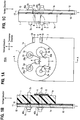
- An optical module 100A illustrated in FIGs. 1A to 1C is an optical module using a TO-CAN package for optical reception according to a first embodiment.
- the optical module 100A includes a stem 1, four lead pins 2a to 2d, glasses 3a to 3d, a photodiode 4 (an element: an optical element), an amplifier 5 (an element: an electrical element), and an FPC 7 (a circuit board: a flexible printed circuit board).
- the photodiode 4 and the amplifier 5 are disposed proximate to each other.
- the optical module 100A of the present embodiment does not include the lead pin 2e serving as the ground pin which the optical module 200 includes.
- the stem 1 in the optical module 100A includes a protrusion 9.
- the FPC 7 includes a ground connection land 18, and the protrusion 9 is soldered and thereby ground-connected to the ground connection land 18.
- the FPC 7 is formed in the shape of a belt which extends in one direction. As illustrated in FIGs. 1A to 1C , the rear main surface 1b of the stem 1 is in contact (for example, in close contact) with a part of the surface of the FPC 7.
- the FPC 7 further includes a portion opposite to the protrusion 9 of the stem 1.
- the ground connection land 18 is a ground-forming land.
- the ground connection land 18 is formed at a position opposite to the protrusion 9 in the FPC 7.
- the ground connection land 18 can be realized, for example, by cutting out the protective layer 19 and the reinforcement plate (not shown) at a position where the ground connection land 18 is formed and exposing the lower layer ground 11. Otherwise, the ground connection land 18 can be realized, for example, by providing a through-hole in the protective layer 19 and the reinforcement plate (not shown).
- a solder 8 makes a ground connection with the stem 1 at a position where the ground connection land 18 is formed.
- the protrusion 9 is disposed on a side surface of the stem 1.
- the protrusion 9 may be formed integrally with the disc of the stem 1, for example by press working.
- the solder 8 serving as an electrical connection means with the ground connection land 18 is attached to the protrusion 9.
- the protrusion 9 of the present embodiment has a thickness similar to one of the stem 1, but is not limited to this.
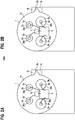
- the protrusion 9 can be formed in various shapes. For example, as illustrated in FIG. 1 , the protrusion 9 can be formed in a rectangular shape (in the shape of a quadrangular prism). Instead, the protrusion 9 can be formed in a triangular shape (in the shape of a triangular prism), as illustrated in FIG. 2A . Otherwise, a curved surface may be provided in each boundary between the protrusion 9 and the main body of the stem 1, as shown in FIG. 2B .
- the ground connection land 18 is disposed on the right side of the stem 1 on the sheet of FIG. 1 .
- the ground connection land 18 may be disposed anywhere in the circumferential direction of the stem 1, and outward of the stem 1 (for example, on the outer edge of the stem 1).
- a benefit of the arrangement of the ground connection land 18 outward of the stem 1, for example on the outer edge of the stem 1, is that the ground connection land 18 can be easily soldered to the stem 1.
- the ground connection land 18 like this makes the fifth lead pin 2e no longer necessary as the ground pin. Therefore, the region in which the ground pin is disposed on the rear main surface 1b of the stem 1 becomes unnecessary, and a diameter of the stem 1 can be designed to be small. As a result, the entire optical module 100A can be reduced in size.
- the ground pin is not required, the weld part 6 ( FIG. 10 ) exiting around the root of the ground pin also becomes unnecessary.
- the high-frequency characteristics can be improved through things such as reductions in inductances of the first and second lead pins 2a, 2b serving as the signal pins, and a transmission speed can be increased.
- a straight line segment between the center of the stem 1 and the center of the ground connection land 18 (a straight line segment extending in the left-right direction on the sheet of FIG. 1 ) is orthogonal to a direction in which the FPC 7 is drawn out from the stem 1 (see arrows in FIG. 1 , and the direction will be sometimes referred to as a "vertical direction"). Because of this, when the FPC 7 is mounted on the mother board 17 by being bent (see FIG. 12 ), the ground connection land 18 does not protrude in the up-down direction in FIG. 12 (such as from the main body of the stem 1 to the mother board 17). The vertical dimension of the optical module 100A can be reduced (low profile mounting on the mother board 17). Incidentally, the direction orthogonal to the vertical direction as illustrated in FIG. 1 will be sometimes referred to as a "transverse direction.” Like in FIG. 1 , the arrows representing the vertical and transverse directions are drawn as appropriate in other drawings.
- the optical module 100A of the present embodiment can improve the heat dissipation performance of the stem 1. This is because the ground connection area between the stem 1 and the FPC 7 can be greatly increased as compared with the comparative example in which the fifth lead pin 2e having a small diameter is used as the ground pin. This makes it easy to deal with the increase in the heat dissipation density accompanied by the size reduction, and accordingly makes it possible to enhance the reliability of the smaller-sized optical module.
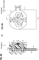
- An optical module 100B illustrated in FIGs. 3A and 3B is an optical module using a TO-CAN package for optical reception according to a second embodiment.
- the photodiode 4 is disposed on the amplifier 5.
- the lead pins 2a to 2d are positioned so as to surround the amplifier 5.
- the direction of the straight line connecting the center of the stem 1 and the center of the ground connection land 18 (or the protrusion 9) is the transverse direction.
- the photodiode 4 By disposing the photodiode 4 on the amplifier 5, the region in which the photodiode 4 is disposed on the front main surface 1a of the stem 1 becomes virtually unnecessary. This makes it possible to minimize the space needed to mount the components, and to design the stem 1 with a smaller diameter. Incidentally, as illustrated in FIG. 3A , the photodiode 4 and the amplifier 5 are disposed at the center of the front main surface 1a of the stem 1.
- the first and second lead pins 2a, 2b for the signals are disposed in the transverse direction such that a space between them is large enough for the amplifier 5 to be mounted between them.
- the third and fourth lead pins 2c, 2d for the biases are disposed in the vertical direction such that a space between them is large enough for the amplifier 5 to be mounted between them.
- the lead pins 2a to 2d may be disposed around the amplifier 5, no matter where the lead pins 2a to 2d are disposed in the circumferential direction of the stem 1. By disposing the lead pins 2a to 2d in this manner, the diameter of the stem 1 can be minimized.
- the protrusion 9 is disposed on the side surface of the stem 1, the protrusion 9 serves as a mark when the FPC 7 is assembled. Therefore, by referring to the protrusion 9, therefore, the manufacturer of the optical module 100A can easily connect the terminals of the stem 1 and the FPC 7 without mistake even when the pin arrangement is centrosymmetric as shown in FIG. 3 .
- An optical module 100C illustrated in FIGs. 5A and 5B is an optical module using a TO-CAN package for optical reception of the present embodiment. What makes the optical module 100C of the present embodiment different from the optical module 100B of the second embodiment is mainly that a flat portion is provided at the outer periphery of the stem 1.
- the optical module 100C is also different from the optical modules 100A, 100B in that: the optical module 100C includes two ground connection lands 18 disposed with the center of the stem 1 interposed therebetween, and two protrusions 9 disposed with the center of the stem 1 interposed therebetween; and the ground connection lands 18 are provided with solders 8, respectively.
- the number of ground connection lands 18 and the number of protrusions 9 in the optical module 100C, as well as the positions of the respective ground connection lands 18 and the positions of the respective protrusions 9 in the circumferential direction of the stem 1 are applicable not only to the present embodiment but also to other embodiments.
- a transverse width of the FPC 7, except for where the ground connection lands 18 exist can be set equal to a transverse width of the stem 1.
- Such a shape is not limited to the present embodiment, and can also be applied to other embodiments.
- the third and fourth lead pins 2c, 2d for the biases are disposed in the vertical direction such that a space between them is large enough for the amplifier 5 to be mounted between them, as described in the second embodiment.
- considerably large unoccupied spaces are respectively formed in the two vertical ends of the stem 1.
- the forming of the flat parts in the respective two vertical ends of the stem 1 makes it possible to further reduce the size of the stem 1.
- the stem 1 is formed in such shape that two portions are cut away from the stem 1 in parallel to a straight line connecting the first and second lead pins 2a, 2b for the signals which are disposed in the transverse direction with the amplifier 5 interposed between them, as well as the ground connection lands 18, 18 and the protrusions 9, 9 are disposed substantially on this straight line.
- the arrangement like this makes it possible to much further reduce the size of the optical module.
- Characteristic impedances of the first and second lead pins 2a, 2b serving as the signal pins are preferably set to an impedance (for example, 50 ⁇ ) matching an output impedance of the amplifier 5.
- impedances of the third and fourth lead pins 2c, 2d for the biases are preferably set low, since the third and fourth lead pins 2c, 2d are connected to an external power supply or the like. Therefore, the glasses 3c, 3d which insulate the third and fourth lead pins 2c, 2d for the biases can have a smaller dimension in the radial direction than the glasses 3a, 3b which insulate the first lead pin 2a and the second lead pin 2b for the signals.
- the first and second lead pins 2a, 2b for the signals are disposed in the transverse direction with the amplifier 5 interposed therebetween, while the third and fourth lead pins 2c, 2d for the biases are disposed in the vertical direction with the amplifier 5 interposed therebetween.
- This arrangement makes it possible to provide the vertical ends of the stem 1 with respective large unoccupied spaces, and to enlarge the notched areas at the two vertical ends of the stem 1.
- the stem 1 is formed in such shape that the portions are cut away from the stem 1 in parallel to the straight line connecting the first and second lead pins 2a, 2b for the signals, the vertical dimension of the stem 1 can be reduced to a large extent.
- the FPC 7 is formed in such shape that as illustrated in FIG. 5A , an upper portion is cut away from the FPC 7 corresponding to the shape of the stem 1, the height of the optical module 100C can be reduced to a large extent.
- the position near the outer side in the radial direction of the third lead pin 2c can be set as the bending position of the FPC 7 (see reference sign C1 in FIG. 6 ).
- the bending position indicated with reference sign C1 is closer to the center of the stem 1 than the bending position (see reference sign B1 in FIG. 4 ) shown in the second embodiment.
- the optical module 100C includes the two ground connection lands 18, the area in which to ground-connect the stem 1 and the FPC 7 can be increased, and the heat dissipation performance of the stem 1 can be enhanced further. This makes it easy to deal with the increase in the heat dissipation density accompanied by the size reduction, and accordingly makes it possible to enhance the reliability of the smaller-sized optical module.
- the ground connection lands 18 (and a portion of the FPC supporting the ground connection lands 18 which is located outside the circular stem main body) may be formed in any shape, as long as the shape enables the ground connection lands 18 to be soldered to the protrusions 9 of the stem 1.
- the ground connection lands 18 may be formed in various shapes including not only a rectangular (quadrangular) one, but also a triangular (triangular prismatic) one which is the shape of the protrusion 9 exemplified in FIG. 2 .
- An optical module 100D illustrated in FIGs. 7A and 7B is an optical module using a TO-CAN package for optical transmission according to the present embodiment.
- the optical module 100D includes a VCSEL (Vertical Cavity Surface Emitting LASER) 30 (a laser diode: an element: an optical element) which is a laser diode, instead of the photodiode 4.
- the optical module 100D has a driver 50 (a driving circuit: an element: an electrical element) instead of the amplifier 5.
- the optical module 100D has three lead pins in total: a single lead pin 2c for a bias instead of the two lead pins for the biases, a lead pin 2a for signal input, and a lead pin 2b for inverted signal input.
- the VCSEL 30 resonates light in a direction perpendicular to the main surface of the stem 1, and emits an optical signal in the perpendicular direction.
- the driver 50 outputs a drive signal in order to make the VCSEL 30 emit the optical signal.
- a signal input terminal of the driver 50 is wire-connected to the lead pin 2a, and an inverted signal input terminal of the driver 50 is wire-connected to the lead pin 2b.
- the output terminals of the driver 50 are wire-connected to the terminals (anode/cathode) of the VCSEL 30.
- optical module 100A functioning as the optical reception system shown in the first embodiment is also applied to the optical module 100D functioning as the optical transmission system shown in the present embodiment.
- the optical module functions as the optical transmission system, the overall size of the optical module can be reduced.
- An optical module 100E illustrated in FIGs. 8A and 8B is an optical module using a TO-CAN package for optical transmission according to a fifth embodiment. There are three differences between the optical module 100E of the present embodiment and the optical module 100D of the fourth embodiment.
- the VCSEL 30 is disposed on the driver 50.
- the lead pins 2a to 2c are positioned so as to surround the driver 50.
- a flat part is provided at an outer periphery of the stem 1.
- the VCSEL 30 and the driver 50 are disposed at the center of the front main surface 1a of the stem 1.
- the first and second lead pins 2a, 2b for the signals are disposed in the transverse direction such that a space between them is large enough for the driver 50 to be mounted between them.
- the single third lead pin 2c for the bias is disposed under the driver 50 on the sheet of FIG. 8A .
- the lead pins 2a to 2c are disposed close to the driver. The arrangement of the lead pins 2a to 2c in this manner makes it possible to minimize the diameter of the stem 1.
- the first and second lead pins 2a, 2b for the signals are disposed in the transverse direction with the driver 50 interposed therebetween. Furthermore, the third lead pin 2c for the bias is disposed under the driver 50 on the sheet of FIG. 8A .
- the stem 1 is formed in such shape that portions are cut away from the stem 1 in parallel to a straight line connecting the first and second lead pins 2a, 2b for the signals. Thus, the vertical dimension of the stem 1 can be reduced to a large extent.
- the FPC 7 is formed in such shape that as illustrated in FIG. 8A , an upper portion is cut away from the FPC 7 corresponding to the shape of the stem 1, a height of the optical module 100E can be reduced to a large extent.
- the optical module 100E of the fifth embodiment is substantially the same as the optical module 100D of the fourth embodiment for explaining an optical transmission system in which the characteristics of the optical modules of the first to third embodiments for explaining an optical reception system are introduced. Therefore, the optical module 100E as an optical transmission system achieves the same effects as the first to third embodiments, and the optical module 100E can be reduced in size, particularly in height in the vertical direction.
- An optical module 100F illustrated in FIGs. 9A and 9B is an optical module using a TO-CAN package for optical transmission of the present embodiment.
- the optical module 100F includes a monitoring photodiode 21 (an element: an optical element) instead of the driver 50.
- the VCSEL 30 and the monitoring photodiode 21 are disposed at the center of the front main surface 1a of the stem 1.
- the VCSEL 30 is disposed on the monitoring photodiode 21.
- the driver is mounted on the mother board to which the FPC 7 is connected (not shown).
- the monitoring photodiode 21 receives a light reflection signal from the cap (not shown) attached to the optical module 100F, and generates an electric current corresponding to an optical transmission power from the VCSEL 30.
- the electric current is sent to the mother board via the FPC 7, and is used by the VCSEL 30 for performing APC (automatic power control) and the like.
- APC automatic power control
- the optical module 100F of the sixth embodiment forms an optical transmission system which is different from that of the optical module 100E of the fifth embodiment.
- the optical module 100F includes four lead pins 2a to 2d in total, two of which are the third and fourth lead pins 2c, 2d for the biases.
- the first and second lead pins 2a, 2b are respectively used to input a signal and an inverted signal into the VCSEL 30, and are wire-connected to the anode and cathode of the VCSEL 30, respectively.
- the third and fourth lead pins 2c, 2d are wire-connected to the anode and cathode of the monitoring photodiode 21, respectively.
- the VCSEL 30 emits an optical signal in the perpendicular direction.
- the third and fourth lead pins 2c, 2d for the biases are disposed in the vertical direction such as a space between them is large enough for the monitoring photodiode 21 to be mounted between them.
- the optical module 100F of the sixth embodiment constitutes an optical transmission system different from that of the optical module 100E of the fifth embodiment, the effects of the fifth embodiment can be realized.
- the optical module 100F of the sixth embodiment serving as the optical transmission system can exert all the same effects as the optical modules of the first to third embodiments, and can achieve a reduction in the size of the optical module 110E, particularly a reduction in its height in the vertical direction.
- An optical module 100G illustrated in FIG. 13 is an optical module using a TO-CAN package for optical reception of the present embodiment.
- a cap 14 including a light-incident window or lens is attached to the stem 1.
- a part called an optical fiber stub 24 is used as an optical connection part 15 (see FIG. 4 ).
- the optical fiber stub 24 is aligned with and fixed to the cap 14.
- the optical fiber stub 24 is a part comprising an optical fiber strand 24a and a cylindrical ceramic 24b.
- the optical fiber stub 24 is formed as a part obtained by: making a hole, having substantially the same diameter as the optical fiber strand 24a, at the center of the cylindrical ceramic 24b excellent in mechanical strength; making the optical fiber strand 24a penetrate through the hole; and thereafter optically polishing the two ends of the optical fiber strand 24a.
- YAG Yittrium Aluminum Garnet
- a part obtained by integrally fixing a cylindrical metal-made flange 22 (an aligning-fixing part) to the optical fiber stub 24 in advance is held by an X-Y two-axis stage (not shown).
- the metal-made flange 22 is a member for aligning the optical fiber stub 24 with the cap 14 and fixing the optical fiber stub 24 to the cap 14.
- the X-Y two-axis stage is a jig for aligning the optical fiber stub 24 with the cap 14 and fixing the optical fiber stub 24 to the cap 14 by the metal made flange 22 with respect to the vertical direction (X) and the transverse direction (Y).
- X vertical direction
- Y transverse direction
- peak alignment is performed on the light emitted from the cap 14 on a horizontal plane (an X-Y plane).
- the metal-made flange 22 is fixed to the cap 14 by YAG laser welding.
- the fixing of the metal-made flange 22 to the optical fiber stub 24 may be performed, for example, by using an epoxy-based adhesive, or by swaging the metal-made flange 22.
- the X-Y two-axis alignment of the optical fiber stub 24 is realized by the above steps.
- a cylindrical metal part called a Z-sleeve 23 (an aligning-fixing part) on the outer periphery of the metal-made flange 22
- Z represents a direction which is perpendicular to the X-Y plane, and which is identical to the direction of the optical axis 16.
- the Z-sleeve 23 is a member for, while fixed to the metal-made flange 22, aligning the optical fiber stub 24 with the cap 14 and fixing the optical fiber stub 24 to the cap 14.
- the fixing of the Z-sleeve 23 to the metal-made flange 22 may be performed, for example, by using an epoxy-based adhesive, or by swaging the Z-sleeve 23.
- the X-Y-Z three-axis alignment can be achieved with the optical fiber stub 24 held by an X-Y-Z three-axis stage (not shown).
- the X-Y-Z three-axis stage is a jig for aligning the optical fiber stub 24 with the cap 14 and fixing the optical fiber stub 24 to the cap 14 with regard to the vertical direction (X), the transverse direction (Y) and the perpendicular direction (Z) with the metal-made flange 22 and Z-sleeve 23.
- peak alignment is performed on the light emitted from the cap 14. Once a peak position is obtained, the metal-made flange 22 is fixed to the cap 14 by YAG laser welding.
- the X-Y-Z three-axis alignment can be achieved, too, by coordinately operating the X-Y stage with the optical fiber stub 24 held thereby, and a Z stage (not shown) with the stem 1 held thereby while the cap 14 is fixed to the stem 1. Either of the two alignment methods can be used.
- the Z stage is a jig for aligning the optical fiber stub 24 with the cap 14 and fixing the optical fiber stub 24 to the cap 14 with respect to the direction (Z) of the optical axis 16.
- the photodiode 4 through which the optical axis 16 of the optical fiber stub 24 passes receives the optical signal inputted from the optical fiber stub 24 with a very high optical coupling rate.
- the FPC 7 includes a pad (not shown) for connecting the FPC 7 to the mother board 17.
- the FPC 7 can therefore send and receive an electrical signal to and from the mother board 17.
- the optical IF (Interface) of the optical module 100G of the present embodiment becomes the optical fiber stub 24, it is necessary to provide a receptacle to an apparatus or the like on the other side.
- This means the configuration of the optical module 100G of the seventh embodiment is to the reverse of the configuration of the optical module disclosed in Patent Literature 1.
- the optical module 100G of the present embodiment since the optical module 100G itself does not have a receptacle, the optical module 100G can be miniaturized and reduced in height. As a result, the optical module 100G of the present embodiment can be miniaturized to a size smaller than that of the receptacle.
- the mating device or the like, which the optical module 100G is optically connected to is required to include a receptacle, the mating device has a higher degree of freedom in the design since the mating device is formed from only passive parts. Overall, reductions in the size and height can be easily achieved. The effect of reducing the size is more obvious in an array configuration and the like using multiple optical modules 100G.
- the stem 1 and the ground connection land 18 are connected to each other by the protrusion 9, but as in the modification (a), the stem 1 and the ground connection land 18 may be directly connected to each other.
- the ground connection land 18 may be provided near the connection part, and is not limited to the outer edge or the outer side of the stem 1.
Landscapes
- Physics & Mathematics (AREA)
- General Physics & Mathematics (AREA)
- Optics & Photonics (AREA)
- Light Receiving Elements (AREA)
- Semiconductor Lasers (AREA)
- Optical Couplings Of Light Guides (AREA)
Applications Claiming Priority (1)
| Application Number | Priority Date | Filing Date | Title |
|---|---|---|---|
| PCT/JP2017/025298 WO2019012607A1 (ja) | 2017-07-11 | 2017-07-11 | 光モジュール |
Publications (3)
| Publication Number | Publication Date |
|---|---|
| EP3667378A1 true EP3667378A1 (de) | 2020-06-17 |
| EP3667378A4 EP3667378A4 (de) | 2020-08-26 |
| EP3667378B1 EP3667378B1 (de) | 2026-04-08 |
Family
ID=65002125
Family Applications (1)
| Application Number | Title | Priority Date | Filing Date |
|---|---|---|---|
| EP17917577.3A Active EP3667378B1 (de) | 2017-07-11 | 2017-07-11 | Optisches modul |
Country Status (6)
| Country | Link |
|---|---|
| US (1) | US11327258B2 (de) |
| EP (1) | EP3667378B1 (de) |
| JP (1) | JP7057357B2 (de) |
| CN (1) | CN110741298B (de) |
| TW (1) | TWI663737B (de) |
| WO (1) | WO2019012607A1 (de) |
Families Citing this family (6)
| Publication number | Priority date | Publication date | Assignee | Title |
|---|---|---|---|---|
| JP7454996B2 (ja) * | 2020-05-11 | 2024-03-25 | CIG Photonics Japan株式会社 | 光モジュール |
| JP7204065B2 (ja) * | 2020-11-24 | 2023-01-13 | 三菱電機株式会社 | 光モジュール |
| JP7542419B2 (ja) * | 2020-12-02 | 2024-08-30 | CIG Photonics Japan株式会社 | 光モジュール |
| JP2022143754A (ja) * | 2021-03-18 | 2022-10-03 | CIG Photonics Japan株式会社 | 光モジュール |
| US12085770B2 (en) * | 2021-10-13 | 2024-09-10 | Electronics And Telecommunications Research Institute | Optical submodule |
| US20250112437A1 (en) * | 2023-09-29 | 2025-04-03 | Keysight Technologies, Inc. | Bandwidth improvement of through-hole distributed feedback laser |
Family Cites Families (33)
| Publication number | Priority date | Publication date | Assignee | Title |
|---|---|---|---|---|
| JP2001296457A (ja) | 1999-10-07 | 2001-10-26 | Sumitomo Electric Ind Ltd | 光送受信器 |
| JP4609818B2 (ja) | 2000-03-31 | 2011-01-12 | 古河電気工業株式会社 | 半導体レーザモジュール |
| US7215886B2 (en) | 2002-02-04 | 2007-05-08 | Hitachi, Ltd. | Optical communication module |
| JP2003241029A (ja) | 2002-02-14 | 2003-08-27 | Sumitomo Electric Ind Ltd | 光モジュールおよび光送受信器 |
| EP1388916A1 (de) | 2002-08-09 | 2004-02-11 | Agilent Technologies, Inc. - a Delaware corporation - | Optoelektronisches Gehäuse |
| JP4586337B2 (ja) | 2002-08-26 | 2010-11-24 | 住友電気工業株式会社 | 半導体レーザモジュールおよび半導体レーザ装置 |
| JP2004349567A (ja) | 2003-05-23 | 2004-12-09 | Kyocera Corp | 半導体素子収納用パッケージおよび半導体装置 |
| US7315698B2 (en) * | 2003-10-22 | 2008-01-01 | Sumitomo Electric Industries, Ltd. | Optical module and an optical receiver using the same |
| JP2005294429A (ja) * | 2004-03-31 | 2005-10-20 | Murata Mfg Co Ltd | 光受信モジュール |
| JP2006351610A (ja) * | 2005-06-13 | 2006-12-28 | Sumitomo Electric Ind Ltd | 光モジュール |
| JP2007042756A (ja) * | 2005-08-01 | 2007-02-15 | Sony Corp | 光デバイスと光通信装置 |
| US20070051877A1 (en) * | 2005-09-06 | 2007-03-08 | Fuji Xerox Co., Ltd. | Optical transmitter-receiver, optical transmitter-receiver module, and optical communication device |
| JP4940628B2 (ja) * | 2005-10-31 | 2012-05-30 | ソニー株式会社 | 光送信モジュール、光送受信モジュール及び光通信装置 |
| JP5076460B2 (ja) * | 2005-12-07 | 2012-11-21 | 住友電気工業株式会社 | サーミスタを搭載した光サブアセンブリ |
| US7467898B2 (en) * | 2006-03-29 | 2008-12-23 | Sumitomo Electric Industries, Ltd. | Optical transceiver installing bi-directional optical sub-assembly |
| JP2008177310A (ja) * | 2007-01-18 | 2008-07-31 | Sumitomo Electric Ind Ltd | 光モジュール及びそれを搭載した光トランシーバ |
| JP5228585B2 (ja) * | 2008-04-08 | 2013-07-03 | 住友電気工業株式会社 | 双方向光モジュール |
| JP5273600B2 (ja) * | 2008-06-17 | 2013-08-28 | 日本オクラロ株式会社 | 光半導体装置 |
| GB2463226B (en) * | 2008-07-22 | 2011-01-12 | Conjunct Ltd | Optical sub-assembly |
| US8145061B2 (en) * | 2009-01-13 | 2012-03-27 | Sumitomo Electric Industries, Ltd. | Optical module implementing a light-receiving device and a light-transmitting device within a common housing |
| TW201113985A (en) * | 2009-06-10 | 2011-04-16 | Coretek Opto Corp | Header structure of opto-electronic element and opto-electronic element using the same |
| TWM375895U (en) * | 2009-08-14 | 2010-03-11 | Ezconn Corp | Light source apparatus |
| US20110085767A1 (en) * | 2009-10-09 | 2011-04-14 | Emcore Corporation | Cooled Laser Module |
| JP5373578B2 (ja) * | 2009-12-15 | 2013-12-18 | 日本電信電話株式会社 | 光モジュール製造方法及び検査方法 |
| US8721193B2 (en) | 2010-08-13 | 2014-05-13 | Finisar Corporation | Electronic module having multiple flex circuit connectors |
| US8723283B2 (en) * | 2011-02-10 | 2014-05-13 | Electronics And Telecommunications Research Institute | Optical module |
| JP2012256692A (ja) * | 2011-06-08 | 2012-12-27 | Mitsubishi Electric Corp | 光モジュール |
| US8913388B2 (en) * | 2012-01-18 | 2014-12-16 | Finisar Corporation | Thermally conductive flexible member for heat transfer |
| JP5958364B2 (ja) * | 2013-01-28 | 2016-07-27 | 日立金属株式会社 | 光モジュール |
| US9063309B2 (en) | 2013-04-22 | 2015-06-23 | Avago Technologies General Ip (Singapore) Pte. Ltd. | Optoelectronic module with flexible substrate |
| JP6445268B2 (ja) * | 2014-07-11 | 2018-12-26 | 日本オクラロ株式会社 | 光モジュール、光送受信モジュール、及びフレキシブル基板 |
| CN105610040A (zh) * | 2014-11-25 | 2016-05-25 | 青岛海信宽带多媒体技术有限公司 | 一种激光发射器 |
| JP6600546B2 (ja) * | 2015-12-11 | 2019-10-30 | 日本ルメンタム株式会社 | 光モジュール |
-
2017
- 2017-07-11 EP EP17917577.3A patent/EP3667378B1/de active Active
- 2017-07-11 JP JP2019529360A patent/JP7057357B2/ja active Active
- 2017-07-11 CN CN201780092007.2A patent/CN110741298B/zh active Active
- 2017-07-11 WO PCT/JP2017/025298 patent/WO2019012607A1/ja not_active Ceased
- 2017-07-11 US US16/629,756 patent/US11327258B2/en active Active
- 2017-08-04 TW TW106126369A patent/TWI663737B/zh active
Also Published As
| Publication number | Publication date |
|---|---|
| CN110741298A (zh) | 2020-01-31 |
| WO2019012607A1 (ja) | 2019-01-17 |
| JPWO2019012607A1 (ja) | 2020-05-21 |
| JP7057357B2 (ja) | 2022-04-19 |
| US11327258B2 (en) | 2022-05-10 |
| CN110741298B (zh) | 2022-11-15 |
| EP3667378B1 (de) | 2026-04-08 |
| EP3667378A4 (de) | 2020-08-26 |
| US20200292764A1 (en) | 2020-09-17 |
| TWI663737B (zh) | 2019-06-21 |
| TW201909436A (zh) | 2019-03-01 |
Similar Documents
| Publication | Publication Date | Title |
|---|---|---|
| EP3667378B1 (de) | Optisches modul | |
| US6940091B2 (en) | Semiconductor laser module and semiconductor laser apparatus | |
| JP5147832B2 (ja) | 光電子パッケージ、サブマウントアセンブリ及び光学サブアセンブリ | |
| US6155724A (en) | Light transmitting module for optical communication and light transmitting unit thereof | |
| US7127142B2 (en) | Optical communication device | |
| US20140099123A1 (en) | Flexible printed circuit board and optical communication module including the same | |
| CN110794524B (zh) | 光学子组件和光学模块 | |
| CN114815093B (zh) | 光模块 | |
| US10295768B2 (en) | Chip on leadframe optical subassembly | |
| US6492698B2 (en) | Flexible circuit with two stiffeners for optical module packaging | |
| JP4212845B2 (ja) | 光半導体素子モジュール | |
| JP2004334189A (ja) | 光モジュール用マウント部材、光モジュール、アレイ型光モジュール、光伝送モジュール | |
| JPWO2005057262A1 (ja) | 光モジュールおよびその製造方法 | |
| US7061025B2 (en) | Optoelectronic device packaging assemblies and methods of making the same | |
| US7004646B2 (en) | Receptacle type optical transmitter and/or receiver module | |
| US7192201B2 (en) | Optical transmitting module having a de-coupling inductor therein | |
| JP6832091B2 (ja) | 光モジュール | |
| US6973227B2 (en) | Optical communication device | |
| US20030161367A1 (en) | Opto-electrical module packaging | |
| JP2005222003A (ja) | マウント、光部品、光送受信モジュール及び双方向光通信モジュール | |
| CN114942493A (zh) | 一种芯片组件、光器件及组装方法 | |
| JP2004309925A (ja) | 光モジュール及びその製造方法、光通信装置、電子機器 | |
| JP4241262B2 (ja) | 発光モジュール | |
| KR20250042342A (ko) | 광 모듈 조립체 | |
| JP2016200622A (ja) | 光配線基板、光モジュール、及び光アクティブケーブル |
Legal Events
| Date | Code | Title | Description |
|---|---|---|---|
| STAA | Information on the status of an ep patent application or granted ep patent |
Free format text: STATUS: THE INTERNATIONAL PUBLICATION HAS BEEN MADE |
|
| PUAI | Public reference made under article 153(3) epc to a published international application that has entered the european phase |
Free format text: ORIGINAL CODE: 0009012 |
|
| STAA | Information on the status of an ep patent application or granted ep patent |
Free format text: STATUS: REQUEST FOR EXAMINATION WAS MADE |
|
| 17P | Request for examination filed |
Effective date: 20200206 |
|
| AK | Designated contracting states |
Kind code of ref document: A1 Designated state(s): AL AT BE BG CH CY CZ DE DK EE ES FI FR GB GR HR HU IE IS IT LI LT LU LV MC MK MT NL NO PL PT RO RS SE SI SK SM TR |
|
| AX | Request for extension of the european patent |
Extension state: BA ME |
|
| A4 | Supplementary search report drawn up and despatched |
Effective date: 20200727 |
|
| RIC1 | Information provided on ipc code assigned before grant |
Ipc: H01S 5/022 20060101ALI20200721BHEP Ipc: G02B 6/42 20060101AFI20200721BHEP |
|
| DAV | Request for validation of the european patent (deleted) | ||
| DAX | Request for extension of the european patent (deleted) | ||
| STAA | Information on the status of an ep patent application or granted ep patent |
Free format text: STATUS: EXAMINATION IS IN PROGRESS |
|
| 17Q | First examination report despatched |
Effective date: 20220919 |
|
| GRAP | Despatch of communication of intention to grant a patent |
Free format text: ORIGINAL CODE: EPIDOSNIGR1 |
|
| STAA | Information on the status of an ep patent application or granted ep patent |
Free format text: STATUS: GRANT OF PATENT IS INTENDED |
|
| INTG | Intention to grant announced |
Effective date: 20251117 |
|
| GRAS | Grant fee paid |
Free format text: ORIGINAL CODE: EPIDOSNIGR3 |
|
| GRAA | (expected) grant |
Free format text: ORIGINAL CODE: 0009210 |
|
| STAA | Information on the status of an ep patent application or granted ep patent |
Free format text: STATUS: THE PATENT HAS BEEN GRANTED |
|
| RAP3 | Party data changed (applicant data changed or rights of an application transferred) |
Owner name: YOKOWO CO., LTD. |
|
| AK | Designated contracting states |
Kind code of ref document: B1 Designated state(s): AL AT BE BG CH CY CZ DE DK EE ES FI FR GB GR HR HU IE IS IT LI LT LU LV MC MK MT NL NO PL PT RO RS SE SI SK SM TR |
|
| REG | Reference to a national code |
Ref country code: CH Ref legal event code: F10 Free format text: ST27 STATUS EVENT CODE: U-0-0-F10-F00 (AS PROVIDED BY THE NATIONAL OFFICE) Effective date: 20260408 Ref country code: GB Ref legal event code: FG4D |
|
| REG | Reference to a national code |
Ref country code: DE Ref legal event code: R096 Ref document number: 602017094754 Country of ref document: DE |