EP3667404A1 - Anzeigetafelmodul und elektronische vorrichtung - Google Patents
Anzeigetafelmodul und elektronische vorrichtung Download PDFInfo
- Publication number
- EP3667404A1 EP3667404A1 EP17928429.4A EP17928429A EP3667404A1 EP 3667404 A1 EP3667404 A1 EP 3667404A1 EP 17928429 A EP17928429 A EP 17928429A EP 3667404 A1 EP3667404 A1 EP 3667404A1
- Authority
- EP
- European Patent Office
- Prior art keywords
- connection area
- panel
- bifurcated
- touch panel
- oled
- Prior art date
- Legal status (The legal status is an assumption and is not a legal conclusion. Google has not performed a legal analysis and makes no representation as to the accuracy of the status listed.)
- Granted
Links
Images






Classifications
-
- H—ELECTRICITY
- H04—ELECTRIC COMMUNICATION TECHNIQUE
- H04M—TELEPHONIC COMMUNICATION
- H04M1/00—Substation equipment, e.g. for use by subscribers
- H04M1/02—Constructional features of telephone sets
- H04M1/0202—Portable telephone sets, e.g. cordless phones, mobile phones or bar type handsets
- H04M1/026—Details of the structure or mounting of specific components
- H04M1/0277—Details of the structure or mounting of specific components for a printed circuit board assembly
-
- H—ELECTRICITY
- H04—ELECTRIC COMMUNICATION TECHNIQUE
- H04M—TELEPHONIC COMMUNICATION
- H04M1/00—Substation equipment, e.g. for use by subscribers
- H04M1/72—Mobile telephones; Cordless telephones, i.e. devices for establishing wireless links to base stations without route selection
- H04M1/724—User interfaces specially adapted for cordless or mobile telephones
- H04M1/72469—User interfaces specially adapted for cordless or mobile telephones for operating the device by selecting functions from two or more displayed items, e.g. menus or icons
-
- G—PHYSICS
- G02—OPTICS
- G02F—OPTICAL DEVICES OR ARRANGEMENTS FOR THE CONTROL OF LIGHT BY MODIFICATION OF THE OPTICAL PROPERTIES OF THE MEDIA OF THE ELEMENTS INVOLVED THEREIN; NON-LINEAR OPTICS; FREQUENCY-CHANGING OF LIGHT; OPTICAL LOGIC ELEMENTS; OPTICAL ANALOGUE/DIGITAL CONVERTERS
- G02F1/00—Devices or arrangements for the control of the intensity, colour, phase, polarisation or direction of light arriving from an independent light source, e.g. switching, gating or modulating; Non-linear optics
- G02F1/01—Devices or arrangements for the control of the intensity, colour, phase, polarisation or direction of light arriving from an independent light source, e.g. switching, gating or modulating; Non-linear optics for the control of the intensity, phase, polarisation or colour
- G02F1/13—Devices or arrangements for the control of the intensity, colour, phase, polarisation or direction of light arriving from an independent light source, e.g. switching, gating or modulating; Non-linear optics for the control of the intensity, phase, polarisation or colour based on liquid crystals, e.g. single liquid crystal display cells
- G02F1/133—Constructional arrangements; Operation of liquid crystal cells; Circuit arrangements
- G02F1/1333—Constructional arrangements; Manufacturing methods
-
- G—PHYSICS
- G06—COMPUTING OR CALCULATING; COUNTING
- G06F—ELECTRIC DIGITAL DATA PROCESSING
- G06F1/00—Details not covered by groups G06F3/00 - G06F13/00 and G06F21/00
- G06F1/16—Constructional details or arrangements
- G06F1/1613—Constructional details or arrangements for portable computers
- G06F1/1633—Constructional details or arrangements of portable computers not specific to the type of enclosures covered by groups G06F1/1615 - G06F1/1626
- G06F1/1637—Details related to the display arrangement, including those related to the mounting of the display in the housing
-
- G—PHYSICS
- G06—COMPUTING OR CALCULATING; COUNTING
- G06F—ELECTRIC DIGITAL DATA PROCESSING
- G06F3/00—Input arrangements for transferring data to be processed into a form capable of being handled by the computer; Output arrangements for transferring data from processing unit to output unit, e.g. interface arrangements
- G06F3/01—Input arrangements or combined input and output arrangements for interaction between user and computer
- G06F3/03—Arrangements for converting the position or the displacement of a member into a coded form
- G06F3/041—Digitisers, e.g. for touch screens or touch pads, characterised by the transducing means
-
- G—PHYSICS
- G06—COMPUTING OR CALCULATING; COUNTING
- G06F—ELECTRIC DIGITAL DATA PROCESSING
- G06F3/00—Input arrangements for transferring data to be processed into a form capable of being handled by the computer; Output arrangements for transferring data from processing unit to output unit, e.g. interface arrangements
- G06F3/01—Input arrangements or combined input and output arrangements for interaction between user and computer
- G06F3/048—Interaction techniques based on graphical user interfaces [GUI]
- G06F3/0481—Interaction techniques based on graphical user interfaces [GUI] based on specific properties of the displayed interaction object or a metaphor-based environment, e.g. interaction with desktop elements like windows or icons, or assisted by a cursor's changing behaviour or appearance
- G06F3/04817—Interaction techniques based on graphical user interfaces [GUI] based on specific properties of the displayed interaction object or a metaphor-based environment, e.g. interaction with desktop elements like windows or icons, or assisted by a cursor's changing behaviour or appearance using icons
-
- G—PHYSICS
- G06—COMPUTING OR CALCULATING; COUNTING
- G06F—ELECTRIC DIGITAL DATA PROCESSING
- G06F3/00—Input arrangements for transferring data to be processed into a form capable of being handled by the computer; Output arrangements for transferring data from processing unit to output unit, e.g. interface arrangements
- G06F3/01—Input arrangements or combined input and output arrangements for interaction between user and computer
- G06F3/048—Interaction techniques based on graphical user interfaces [GUI]
- G06F3/0481—Interaction techniques based on graphical user interfaces [GUI] based on specific properties of the displayed interaction object or a metaphor-based environment, e.g. interaction with desktop elements like windows or icons, or assisted by a cursor's changing behaviour or appearance
- G06F3/0482—Interaction with lists of selectable items, e.g. menus
-
- H—ELECTRICITY
- H04—ELECTRIC COMMUNICATION TECHNIQUE
- H04W—WIRELESS COMMUNICATION NETWORKS
- H04W4/00—Services specially adapted for wireless communication networks; Facilities therefor
- H04W4/60—Subscription-based services using application servers or record carriers, e.g. SIM application toolkits
-
- H—ELECTRICITY
- H05—ELECTRIC TECHNIQUES NOT OTHERWISE PROVIDED FOR
- H05K—PRINTED CIRCUITS; CASINGS OR CONSTRUCTIONAL DETAILS OF ELECTRIC APPARATUS; MANUFACTURE OF ASSEMBLAGES OF ELECTRICAL COMPONENTS
- H05K1/00—Printed circuits
- H05K1/18—Printed circuits structurally associated with non-printed electric components
- H05K1/189—Printed circuits structurally associated with non-printed electric components characterised by the use of flexible or folded printed circuits
-
- H—ELECTRICITY
- H04—ELECTRIC COMMUNICATION TECHNIQUE
- H04M—TELEPHONIC COMMUNICATION
- H04M1/00—Substation equipment, e.g. for use by subscribers
- H04M1/02—Constructional features of telephone sets
- H04M1/0202—Portable telephone sets, e.g. cordless phones, mobile phones or bar type handsets
- H04M1/026—Details of the structure or mounting of specific components
- H04M1/0266—Details of the structure or mounting of specific components for a display module assembly
-
- H—ELECTRICITY
- H04—ELECTRIC COMMUNICATION TECHNIQUE
- H04M—TELEPHONIC COMMUNICATION
- H04M2250/00—Details of telephonic subscriber devices
- H04M2250/22—Details of telephonic subscriber devices including a touch pad, a touch sensor or a touch detector
-
- H—ELECTRICITY
- H05—ELECTRIC TECHNIQUES NOT OTHERWISE PROVIDED FOR
- H05K—PRINTED CIRCUITS; CASINGS OR CONSTRUCTIONAL DETAILS OF ELECTRIC APPARATUS; MANUFACTURE OF ASSEMBLAGES OF ELECTRICAL COMPONENTS
- H05K1/00—Printed circuits
- H05K1/02—Details
- H05K1/14—Structural association of two or more printed circuits
- H05K1/147—Structural association of two or more printed circuits at least one of the printed circuits being bent or folded, e.g. by using a flexible printed circuit
-
- H—ELECTRICITY
- H05—ELECTRIC TECHNIQUES NOT OTHERWISE PROVIDED FOR
- H05K—PRINTED CIRCUITS; CASINGS OR CONSTRUCTIONAL DETAILS OF ELECTRIC APPARATUS; MANUFACTURE OF ASSEMBLAGES OF ELECTRICAL COMPONENTS
- H05K2201/00—Indexing scheme relating to printed circuits covered by H05K1/00
- H05K2201/05—Flexible printed circuits [FPCs]
- H05K2201/052—Branched
-
- H—ELECTRICITY
- H05—ELECTRIC TECHNIQUES NOT OTHERWISE PROVIDED FOR
- H05K—PRINTED CIRCUITS; CASINGS OR CONSTRUCTIONAL DETAILS OF ELECTRIC APPARATUS; MANUFACTURE OF ASSEMBLAGES OF ELECTRICAL COMPONENTS
- H05K2201/00—Indexing scheme relating to printed circuits covered by H05K1/00
- H05K2201/10—Details of components or other objects attached to or integrated in a printed circuit board
- H05K2201/10007—Types of components
- H05K2201/10128—Display
Definitions
- This application relates to the field of electronic products, and in particular, to a narrow bezel display panel module and an electronic device.
- a product bezel becomes a key challenge, and how to reduce a bezel size of a display panel module has become an essential point.
- FIG. 1(a) An out-terminal (PIN) side bezel of an active matrix/organic light emitting diode (active matrix organic light emitting diode, AMOLED) panel is shown in FIG. 1(a) .
- the out-PIN side bezel is located at a lower part of the AMOLED panel, that is, the bottom of a mobile terminal.
- the out-PIN side bezel includes three parts of the panel: a signal wiring area, a chip on film (chip on film, COF) connection region, and a COF bending area, as shown in FIG. 1(b) .
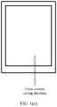
- a cutting direction of the cross section shown in FIG. 1(b) is shown in FIG. 1(c) .
- a touch panel (touch panel) is bonded to the organic light-emitting diode (organic light-emitting diode, OLED) panel by using an optically clear adhesive (optically clear adhesive, OCA).
- OCA optically clear adhesive
- the touch panel and the OLED panel are both connected to a main FPC.
- the touch panel is connected to the main FPC by using a touch-control FPC, and the OLED panel is connected to the main FPC by using a COF.
- the touch panel Seen from a configuration of the display panel module, the touch panel is disposed on an outer side of the OLED panel. In the COF bending area, the touch-control FPC is also bent on an outer side of the COF.
- the out-PIN side bezel is relatively wide.
- Embodiments of the present invention provide a display panel module and an electronic device.
- a touch panel connection area and an OLED panel are connected to a bifurcated COF, thereby reducing a width of an out-PIN side bezel of the display panel module.
- a display panel module may include an organic light-emitting diode OLED panel, a touch panel, and a bifurcated chip on film COF.
- An OLED panel connection area is disposed at a first location on a first side of the OLED panel, a touch panel connection area is disposed at a first location on a first side of the touch panel, and the OLED panel connection area and the touch panel connection area are located at a same side of the display panel module.
- One bifurcated terminal of a bifurcated end of the bifurcated COF is connected to the OLED panel connection area, and the other bifurcated terminal of the bifurcated end of the bifurcated COF is connected to the touch panel connection area.
- the other end of the bifurcated COF is connected to a main flexible printed circuit FPC.
- a chip of the bifurcated chip on film COF is a touch and display driver chip.
- the first location on the first side of the OLED panel is a middle location on the first side of the OLED panel, and the first location on the first side of the touch panel is locations at two ends of the first side of the touch panel; or the first location on the first side of the OLED panel and the first location on the first side of the touch panel are respectively at two ends of a first side of the display panel module.
- the OLED panel connection area is disposed at the first location on the first side of the OLED panel in a fan-like shape.
- a second location on the first side of the touch panel is disposed as an opening area, and a location of the OLED panel connection area is corresponding to the second location after the touch panel is bonded to the OLED panel, to expose the OLED panel connection area after the OLED panel is bonded to the touch panel.
- a distance D is kept between the OLED panel connection area and the touch panel connection area, to avoid signal interference between the touch panel and the OLED panel.
- the distance D is any value between 0.05 mm and 15 mm.
- a width of the OLED panel connection area is W, and the width W is any value between 20 mm and 70 mm.
- the height difference T is any value between 0.01 mm and 2 mm.
- the bifurcated COF is a flexible circuit board to which the touch and display driver chip is bonded.
- a manufacturing method of a display panel module is provided, and the method may include:
- the OLED panel connection area is disposed at a first location on a first side of the OLED panel
- the touch panel connection area is disposed at a first location on a first side of the touch panel
- the first side of the OLED panel and the first side of the touch panel are at a same side of the display panel module.
- Connecting the bifurcated COF to the touch panel and the OLED panel reduces a width of an out-PIN side bezel of the display panel module, thereby improving user experience.
- the first location on the first side of the OLED panel is a middle location on the first side of the OLED panel, and the first location on the first side of the touch panel is locations at two ends of the first side of the touch panel; or the first location on the first side of the OLED panel and the first location on the first side of the touch panel are respectively at two ends of the display panel module.
- the OLED panel connection area is disposed at the first location on the first side of the OLED panel in a fan-like shape.
- the method before the connecting an OLED panel connection area of an organic light-emitting diode OLED panel bonded to a touch panel to one bifurcated terminal of a bifurcated end of a bifurcated chip on film COF, and connecting a touch panel connection area of the touch panel to the other bifurcated terminal of the bifurcated end of the bifurcated COF, the method includes:
- a distance D is kept between the OLED panel connection area and the touch panel connection area, to avoid signal interference between the touch panel and the OLED panel.
- the distance D is any value between 0.05 mm and 15 mm.
- a width of the OLED panel connection area is W, and the width W is any value between 20 mm and 70 mm.
- the height difference T is any value between 0.01 mm and 2 mm.
- an electronic device may include a display panel module and a processor.
- the display panel module includes an organic light-emitting diode OLED panel, a touch panel, and a bifurcated chip on film COF.
- An OLED panel connection area is disposed at a first location on a first side of the OLED panel
- a touch panel connection area is disposed at a first location on a first side of the touch panel
- the OLED panel connection area and the touch panel connection area are located at a same side of the display panel module.
- One bifurcated terminal of a bifurcated end of the bifurcated COF is connected to the OLED panel connection area, and the other bifurcated terminal of the bifurcated end of the bifurcated COF is connected to the touch panel connection area.
- the other end of the bifurcated COF is connected to the processor by using a flexible circuit board.
- a chip of the bifurcated chip on film COF is a touch and display driver chip.
- the first location on the first side of the OLED panel is a middle location on the first side of the OLED panel, and the first location on the first side of the touch panel is locations at two ends of the first side of the touch panel; or the first location on the first side of the OLED panel and the first location on the first side of the touch panel are respectively at two ends of a first side of the display panel module.
- the OLED panel connection area is disposed at the first location on the first side of the OLED panel in a fan-like shape.
- a second location on the first side of the touch panel is disposed as an opening area, and a location of the OLED panel connection area is corresponding to the second location after the touch panel is bonded to the OLED panel, to expose the OLED panel connection area after the OLED panel is bonded to the touch panel.
- a distance D is kept between the OLED panel connection area and the touch panel connection area, to avoid signal interference between the touch panel and the OLED panel.
- the distance D is any value between 0.05 mm and 15 mm.
- a width of the OLED panel connection area is W, and the width W is any value between 20 mm and 70 mm.
- the height difference T is any value between 0.01 mm and 2 mm.
- the bifurcated COF is a flexible circuit board FPC to which the touch and display driver chip is bonded.
- the electronic device is a mobile phone or a wearable device.
- the display panel and the OLED panel are connected to the bifurcated COF, thereby reducing a width of an out-PIN side bezel of the display panel module.
- Embodiments of the present invention provide a display panel module and a manufacturing method thereof, and an electronic device, and are applicable to a display panel module with an OLED panel and an external touch panel bonded to each other.
- the OLED panel may be bonded to the touch panel by using an OCA.
- the OLED panel and the touch panel are designed in a staggered pattern, and a bifurcated COF (Chip On Film, or Chip On Flex, COF for short, where COF represents chip on film) is used to connect the OLED panel and the touch panel, thereby reducing a width of an out-PIN side bezel of a terminal.
- COF Chip On Film, or Chip On Flex, COF for short, where COF represents chip on film
- FIG. 2 is a schematic diagram of a cross section of an out-PIN side bezel of a display panel module of a terminal, and a cutting direction is shown in FIG. 1(c) .
- the display panel module includes an active area (active area), a panel signal line area (panel signal line area), a COF connection region, and a COF bending area.
- a signal line of the active area is connected to a bifurcated chip on film COF in the COF connection region through the panel signal line area, and the bifurcated COF is bent in the COF bending area and is connected to a main flexible printed circuit (flexible printed circuit, FPC), thereby reducing a width of an out-PIN side bezel of a display panel.
- FPC flexible printed circuit
- a chip of the bifurcated chip on film COF is a touch and display driver chip (touch and display driver integration, TDDI).
- the touch and display driver chip includes a touch driver and a display driver, and the touch driver and the display driver are integrated as one piece.
- the bifurcated chip on film COF may be an FPC to which the touch and display driver chip is bonded.
- the active area is an active area of a panel, and the panel includes an OLED panel 10 and a touch panel 20.
- the active area herein may be an active area of a display screen of the terminal, for example, a display screen of a mobile phone. Signal lines of all signals of the active area may be disposed in the panel signal line area.
- the panel signal line area is a bonding lead (bonding lead) area that connects all of the signal lines of the active area to the panel.
- the bonding lead area herein is included in the panel signal line area.
- An OLED panel connection area 40 is disposed at an end of a side of the OLED panel 10; a touch panel connection area 50 is disposed at an end of a side of the touch panel 20; and the OLED panel connection area 40 and the touch panel connection area are disposed at a same side of the display panel module.
- the COF connection area 60 is disposed at a bifurcated end of the bifurcated COF 30. In this embodiment of this application, the COF connection area 60 may also be referred to as a bifurcated end.
- the OLED panel 10 is connected to one bifurcated terminal of the bifurcated end of the bifurcated COF 30 through the OLED panel connection area 40, and the touch panel 20 is connected to the other bifurcated terminal of the bifurcated end of the bifurcated COF 30 through the touch panel connection area 50.
- the bifurcated COF is shown in FIG. 2 .
- the other end of the bifurcated COF 30 is connected to the main FPC.
- a substrate of the bifurcated COF may be polyimide (Polyimide, PI). Because the PI can be bent, the bifurcated COF that connects the OLED panel and the touch panel is bent in the COF bending area, and finally connects the bonding lead on the panel and the main FPC.
- PI Polyimide
- the OLED panel is connected to the touch panel by using the bifurcated COF.
- bending of the bifurcated COF reduces a width of an out-PIN side bezel of the display panel module, thereby further improving user experience.
- the OLED panel and the touch panel are designed in a staggered pattern.
- FIG. 4(a) and descriptions of FIG. 4(a) refer to FIG. 4(a) and descriptions of FIG. 4(a) .
- the TDDI is configured to control both a display function and a touch function of the display panel module.
- the TDDI is configured to control a touch operation on the display panel module, process signals transmitted by an application processor (Application Processor, AP), and control each pixel on the display screen.
- the main FPC is configured to connect the OLED panel and the touch panel (that is, the display screen and a touchscreen) to a main board of the terminal.
- the main board of the terminal may be a PCB provided with an application processor.
- a display panel integrated circuit touch panel integrated circuit, TPIC
- a display driver integrated circuit display driving integrated circuit, DDIC
- COF display driving integrated circuit
- an end, of the AMOLED panel, at which the out-PIN side bezel of the AMOLED panel is located may be referred to as a first end of the display panel module.
- the touch panel connection area an area in which the touch panel is connected to the bifurcated COF
- the OLED connection area an area in which the OLED panel is connected to the bifurcated COF
- a corresponding area in which the bifurcated COF 30 is connected to the touch panel connection area 50 and the OLED panel connection area 40 may be referred to as the COF connection area (COF bonding pad).
- COF bonding pad There are a large quantity of metal wires in the bonding pad, which are similar to connecting fingers (connecting finger).
- the OLED panel connection area and the touch panel connection area are disposed at an out-PIN bezel side of the display panel module.
- the following describes a staggered-pattern design of an OLED panel and a touch panel, a design of a bifurcated COF, and a manner of connecting the bifurcated COF to the OLED panel and the touch panel, in a display panel module.
- FIG. 3(a) is a schematic structural diagram of disposition of an OLED panel connection area according to an embodiment of the present invention.
- FIG. 3(b) is a schematic structural diagram of disposition of a touch panel connection area according to an embodiment of the present invention.
- FIG. 3(c) is a schematic structural diagram after a touch panel is bonded to an OLED panel according to an embodiment of the present invention.
- an OLED panel connection area 40 is narrowed in a fanout (fanout) manner through signal lines of an OLED panel 10, and is disposed at a middle location on an out-PIN side bezel.
- a width of the OLED panel connection area 40 may be W.
- a value of the width W may be determined based on factors such as a size of the OLED panel and/or a resolution of the OLED panel.
- the width W may be any value between 20 mm and 70 mm.
- a touch panel connection area 50 is disposed at two ends of the out-PIN side bezel through a signal line layout.
- the OLED panel connection area 40 there is no signal line layout area on an out-PIN side of the touch panel, and an area corresponding to the OLED panel connection area is disposed as an opening area 70, to expose the OLED panel connection area 40 after the touch panel 20 is bonded to the OLED panel 10, as shown in FIG. 3(c) .
- the OLED panel connection area 40 may be exposed through the opening area 70 disposed on the touch panel, as shown in FIG. 3(c) .
- there is a distance D between the OLED panel connection area 40 and the touch panel connection area 50 is any value between 0.05 mm and 15 mm. A value of the distance D may be determined based on factors such as a size of the OLED panel and/or a resolution of the OLED panel.
- FIG. 4(a) is a schematic structural diagram of another cross section of a display panel module according to an embodiment of the present invention.
- FIG. 4(b) is a schematic diagram of a cutting direction of a cross section shown in FIG. 4(a) .
- the height difference T between the OLED panel connection area 40 and the touch panel connection area 50 may also be affected by some other materials that make up the display panel module, for example, an OCA and a cyclo-olefin polymer (Cyclo-Olefin Polymer, COP).
- OCA cyclo-olefin Polymer
- COP cyclo-olefin Polymer
- the COF connection area is disposed based on locations corresponding to the OLED panel connection area 40 and the touch panel connection area 50.
- a corresponding mark (mark) is set for a connection area corresponding to each section.
- a corresponding connection area width is kept, and the distance D is kept between the OLED panel connection area 40 and the touch panel connection area 50.
- Keeping the distance D between the OLED connection area 40 and the touch panel connection area 50 has at least two advantages.
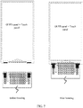
- the COF connection area may be configured as a structure shown in FIG. 6 , which is in a shape of an inverted convex structure.
- the COF connection area 60 may also be referred to as a COF ram.
- a step height of such an inverted convex structure of the COF ram is T, which is kept consistent with the height difference T between the touch panel connection area 50 and the OLED panel connection area 40.
- a middle boss height of the COF ram is greater than the width W of the OLED panel connection area, and less than a sum of the distance D between the touch panel connection area and the OLED panel connection area and the width W of the OLED panel connection area, that is, W ⁇ boss width ⁇ D+W.
- FIG. 7 is a schematic structural diagram before and after the COF connection area 60 is bonded with the OLED panel connection area 40 and the touch panel connection area 50.
- FIG. 8 is a schematic structural diagram of a cross section after the COF connection area 60 is bonded with the OLED panel connection area 40 and the touch panel connection area 50.
- a display panel module in another embodiment, includes an organic light-emitting diode OLED panel, a touch panel, and a bifurcated chip on film COF.
- An OLED panel connection area is disposed at a first location on a first side of the OLED panel
- a touch panel connection area is disposed at a first location on a first side of the touch panel.
- One bifurcated terminal of a bifurcated end of the bifurcated COF is connected to the OLED panel connection area, and the other bifurcated terminal of the bifurcated end of the bifurcated COF is connected to the touch panel connection area.
- the other end of the bifurcated COF is connected to an FPC.
- the touch panel connection area may be disposed at one end side of an out-PIN side of the display panel module, and the OLED panel connection area is disposed at the other end side of the out-PIN side of the display panel module, as shown in FIG. 9 .
- a cutting direction of a cross section shown in FIG. 9 is the same as the direction shown in FIG. 4(b) . Both the one end side and the other end side of the out-PIN side of the display panel module are located at the out-PIN side of the display panel module.
- a width of the OLED panel connection area is still W.
- a value of W may be any value between 20 mm and 70 mm. The value of W may be determined based on factors such as a size of the OLED panel and/or a resolution of the OLED panel.
- a height difference between the touch panel connection area and the OLED panel connection area may still be T. The height difference T may be any value between 0.01 mm and 2 mm. A specific value of the height difference T may be determined based on factors such as a thickness of an OCA that bonds the OLED panel to the touch panel, and a thickness of another material that makes up a display panel.
- a distance D may still be kept between the touch panel connection area and the OLED panel connection area.
- a value of the distance D may be any value between 0.05 mm and 15 mm.
- the value of the distance D may be determined based on factors such as a size of the OLED panel and/or a resolution of the OLED panel.
- a COF connection area namely, a COF ram
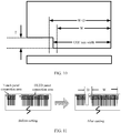
- a width of the COF ram is greater than a width W of an OLED panel connection area, and less than a sum of the width W of the OLED panel connection area and a distance D between the OLED panel connection area and a touch panel connection area, that is, W ⁇ COF ram width ⁇ W+D.
- the COF connection area needs to be slotted to provide a spacing D, as shown in FIG. 11 , and is adapted to a height difference T that originally exists between the touch panel connection area and the OLED connection area.
- FIG. 12 is a schematic flowchart of a manufacturing method of a display panel module according to an embodiment of the present invention. As shown in FIG. 12 , the method may include the following steps.
- a chip of the bifurcated chip on film COF is a touch and display driver chip (touch and display driver integration, TDDI).
- the touch and display driver chip includes a touch driver and a display driver, and the touch driver and the display driver are integrated as one piece.
- the bifurcated chip on film COF may be an FPC to which the touch and display driver chip is bonded.
- the OLED panel connection area disposed at a first location on a first side of the OLED panel is connected to the bifurcated terminal of the bifurcated end of the bifurcated COF, and the touch panel connection area disposed at a first location on a first side of the touch panel is connected to the other bifurcated terminal of the bifurcated end of the bifurcated COF.
- the first side of the OLED panel and the first side of the touch panel are a same side of the display panel module.
- the touch panel connection area may be disposed at two ends of an out-PIN side bezel, and the OLED panel connection area may be disposed at a middle location on the out-PIN side bezel.
- the touch panel connection area may be disposed at one end of an out-PIN side bezel, and the OLED panel connection area may be disposed at the other end of the out-PIN side bezel.
- the bifurcated end of the bifurcated COF may be referred to as a COF ram.
- a structure of the bifurcated end of the COF may be configured based on locations of the touch panel connection area and the OLED panel connection area, and may be specifically a structure shown in FIG. 6 or FIG. 10 .
- the bifurcated COF After the bifurcated COF is connected to the FPC, the bifurcated COF is bent. Using the bifurcated COF reduces a width of an out-PIN side bezel of the display panel module, thereby further improving user experience.
- S1201 and S1202 may be performed in any sequence. This is not limited in this embodiment of the present invention.
- the method further includes the following step:
- the touch panel may be bonded to the OLED panel by using an OCA.
- the connection area of the bonded OLED panel is exposed through an opening area disposed on the touch panel, for example, the opening area 70 shown in FIG. 3(b) .
- a distance D may be kept between the touch panel connection area and the OLED panel connection area.
- a value of the distance D may be any value between 0.05 mm and 15 mm. The value of the distance D may be determined based on factors such as a size of the OLED panel and/or a resolution of the OLED panel.
- a width of the OLED panel connection area may be W.
- a value of W may be any value between 20 mm and 70 mm.
- the value of W may be determined based on factors such as a size of the OLED panel and/or a resolution of the OLED panel.
- the height difference T may be any value between 0.01 mm and 2 mm.
- a specific value of the height difference T may be determined based on factors such as a thickness of an OCA that bonds the OLED panel to the touch panel, and a thickness of another material that makes up a display panel.
- An embodiment of the present invention further provides an electronic device.
- the electronic device may include a display panel module and a processor described in any one of the foregoing embodiments.
- the display panel module includes an organic light-emitting diode OLED panel, a touch panel, and a bifurcated chip on film COF.
- An OLED panel connection area is disposed at a first location on a first side of the OLED panel, and a touch panel connection area is disposed at a first location on a first side of the touch panel.
- the OLED panel connection area and the touch panel connection area are located at a same side of the display panel module.
- One bifurcated terminal of a bifurcated end of the bifurcated COF is connected to the OLED panel connection area, and the other bifurcated terminal of the bifurcated end of the bifurcated COF is connected to the touch panel connection area.
- the other end of the bifurcated COF is connected to the processor by using an FPC.
- a chip of the bifurcated chip on film COF is a touch and display driver chip.
- the first location on the first side of the OLED panel is a middle location on the OLED panel
- the first location on the first side of the touch panel is locations at two ends of the first side of the touch panel.
- the first location on the first side of the OLED panel and the first location on the first side of the touch panel are respectively at two ends of a first side of the display panel module.
- the OLED panel connection area is disposed at the first location on the first side of the OLED panel in a fan-like shape.
- a second location on the first side of the touch panel is disposed as an opening area, and a location of the OLED panel connection area is corresponding to the second location after the touch panel is bonded to the OLED panel, to expose the OLED panel connection area after the OLED panel is bonded to the touch panel.
- a distance D is kept between the OLED panel connection area and the touch panel connection area, and the distance D is any value between 0.05 mm and 15 mm.
- a width of the OLED panel connection area is W, and the width W is any value between 20 mm and 70 mm.
- the height difference T is any value between 0.01 mm and 2 mm.
- the bifurcated COF is a flexible circuit board FPC to which the touch and display driver chip is bonded.
- the electronic device is a mobile phone or a wearable device.
Landscapes
- Engineering & Computer Science (AREA)
- Theoretical Computer Science (AREA)
- Physics & Mathematics (AREA)
- General Engineering & Computer Science (AREA)
- Human Computer Interaction (AREA)
- General Physics & Mathematics (AREA)
- Signal Processing (AREA)
- Computer Networks & Wireless Communication (AREA)
- Nonlinear Science (AREA)
- Computer Hardware Design (AREA)
- Microelectronics & Electronic Packaging (AREA)
- Chemical & Material Sciences (AREA)
- Crystallography & Structural Chemistry (AREA)
- Mathematical Physics (AREA)
- Optics & Photonics (AREA)
- Electroluminescent Light Sources (AREA)
- Devices For Indicating Variable Information By Combining Individual Elements (AREA)
Applications Claiming Priority (2)
| Application Number | Priority Date | Filing Date | Title |
|---|---|---|---|
| CN201710929973 | 2017-10-09 | ||
| PCT/CN2017/109163 WO2019071671A1 (zh) | 2017-10-09 | 2017-11-02 | 一种显示面板模组和电子设备 |
Publications (3)
| Publication Number | Publication Date |
|---|---|
| EP3667404A1 true EP3667404A1 (de) | 2020-06-17 |
| EP3667404A4 EP3667404A4 (de) | 2020-12-02 |
| EP3667404B1 EP3667404B1 (de) | 2022-02-23 |
Family
ID=66101240
Family Applications (1)
| Application Number | Title | Priority Date | Filing Date |
|---|---|---|---|
| EP17928429.4A Active EP3667404B1 (de) | 2017-10-09 | 2017-11-02 | Anzeigetafelmodul und elektronische vorrichtung |
Country Status (4)
| Country | Link |
|---|---|
| US (1) | US11039006B2 (de) |
| EP (1) | EP3667404B1 (de) |
| CN (1) | CN109906403A (de) |
| WO (1) | WO2019071671A1 (de) |
Families Citing this family (6)
| Publication number | Priority date | Publication date | Assignee | Title |
|---|---|---|---|---|
| KR20200123819A (ko) | 2018-03-31 | 2020-10-30 | 후아웨이 테크놀러지 컴퍼니 리미티드 | 디스플레이 장치, 디스플레이 장치 제조 방법 및 전자 기기 |
| KR102599722B1 (ko) * | 2018-12-28 | 2023-11-09 | 삼성디스플레이 주식회사 | 표시 패널 및 이를 포함하는 타일드 표시 장치 |
| US11698695B2 (en) | 2019-06-27 | 2023-07-11 | Chengdu Boe Optoelectronics Technology Co., Ltd. | Chip on flex, touch assembly, and display device |
| CN113703602B (zh) * | 2020-05-22 | 2024-10-18 | 联咏科技股份有限公司 | Oled触控显示芯片及包含其的oled触控显示装置 |
| CN113050331B (zh) * | 2021-03-31 | 2022-05-31 | 武汉华星光电技术有限公司 | 一种无边框液晶显示面板 |
| EP4454436A4 (de) | 2022-05-20 | 2025-01-22 | Boe Technology Group Co., Ltd. | Anzeigegerät |
Family Cites Families (15)
| Publication number | Priority date | Publication date | Assignee | Title |
|---|---|---|---|---|
| JP2005038231A (ja) * | 2003-07-16 | 2005-02-10 | Kawaguchiko Seimitsu Co Ltd | 画面入力型表示装置 |
| KR20050032894A (ko) * | 2003-10-02 | 2005-04-08 | 하현명 | 휴대용 전자기기의 배터리 대용 전원공급장치 |
| JP4809783B2 (ja) | 2007-01-26 | 2011-11-09 | 株式会社 日立ディスプレイズ | タッチパネル付き表示モジュール |
| CN102566837A (zh) * | 2010-12-17 | 2012-07-11 | 东莞联胜液晶显示器有限公司 | 触控显示装置 |
| US9084368B2 (en) | 2011-06-15 | 2015-07-14 | Novatek Microelectronics Corp. | Single FPC board for connecting multiple modules and touch sensitive display module using the same |
| TW201438349A (zh) * | 2011-06-15 | 2014-10-01 | Novatek Microelectronics Corp | 連接多模組之單片式軟性電路板及應用其之觸控顯示模組 |
| WO2013094975A1 (en) * | 2011-12-23 | 2013-06-27 | Samsung Electronics Co., Ltd. | Display module and display apparatus having the same |
| KR102223125B1 (ko) * | 2014-03-27 | 2021-03-05 | 삼성디스플레이 주식회사 | 데이터 구동부 및 이를 구비한 표시 장치 |
| CN106155370B (zh) * | 2015-03-23 | 2019-06-21 | 群创光电股份有限公司 | 触控装置 |
| CN104731414B (zh) * | 2015-04-07 | 2019-01-11 | 武汉华星光电技术有限公司 | 触控显示装置及电子设备 |
| CN104992956B (zh) | 2015-05-15 | 2018-11-09 | 深圳市华星光电技术有限公司 | 无边框显示装置及其制作方法 |
| CN105630244B (zh) * | 2016-01-06 | 2019-01-15 | 武汉华星光电技术有限公司 | 触控显示装置 |
| CN106293233A (zh) * | 2016-08-12 | 2017-01-04 | 武汉华星光电技术有限公司 | 触控显示器的驱动方法及驱动系统 |
| CN106504647B (zh) * | 2016-10-31 | 2019-03-19 | 昆山国显光电有限公司 | 一种oled模组 |
| CN106526925A (zh) * | 2016-11-25 | 2017-03-22 | 上海天马微电子有限公司 | 一种显示模组和显示装置 |
-
2017
- 2017-11-02 WO PCT/CN2017/109163 patent/WO2019071671A1/zh not_active Ceased
- 2017-11-02 US US16/652,474 patent/US11039006B2/en active Active
- 2017-11-02 EP EP17928429.4A patent/EP3667404B1/de active Active
- 2017-11-02 CN CN201780066041.2A patent/CN109906403A/zh active Pending
Also Published As
| Publication number | Publication date |
|---|---|
| CN109906403A (zh) | 2019-06-18 |
| US20200236213A1 (en) | 2020-07-23 |
| EP3667404A4 (de) | 2020-12-02 |
| US11039006B2 (en) | 2021-06-15 |
| EP3667404B1 (de) | 2022-02-23 |
| WO2019071671A1 (zh) | 2019-04-18 |
Similar Documents
| Publication | Publication Date | Title |
|---|---|---|
| US11039006B2 (en) | Display panel module and electronic device | |
| US10761656B2 (en) | Display device | |
| CN108052233B (zh) | 一种显示面板和显示装置 | |
| KR101661160B1 (ko) | 터치 스크린 패널 장치 | |
| US11515367B2 (en) | Display apparatus, method for manufacturing display apparatus, and electronic device | |
| KR102457907B1 (ko) | 표시 장치 | |
| CN105700728B (zh) | 电子显示模块及电子装置 | |
| KR20150114195A (ko) | 터치 패널 및 이를 포함하는 터치 디바이스 | |
| CN107665057B (zh) | 触控显示设备 | |
| US8878798B2 (en) | Touch screen panel display | |
| CN109378334B (zh) | 一种oled显示装置及其制备方法 | |
| CN110164913B (zh) | 一种显示模组及其制作方法、显示装置 | |
| US12530096B2 (en) | Chip on flex | |
| CN110187580B (zh) | 显示面板及其制作方法、显示装置 | |
| CN115019677A (zh) | 显示面板及其制备方法、显示装置的制备方法 | |
| KR102388802B1 (ko) | 터치표시장치 | |
| CN106843606A (zh) | 触控传感器、触控面板和电子设备 | |
| KR20150031805A (ko) | 터치패널 | |
| CN115633530A (zh) | 显示面板及显示装置 | |
| US11133432B2 (en) | Display panel and manufacturing method thereof, and display device | |
| KR20150066860A (ko) | 터치 센서 일체형 평판 표시장치 | |
| US10852869B2 (en) | Narrow border touch display apparatus | |
| CN119486518A (zh) | 显示模组,显示装置及显示模组的制备方法 | |
| CN112596639A (zh) | 触控显示装置 | |
| KR20220030412A (ko) | 표시 장치 |
Legal Events
| Date | Code | Title | Description |
|---|---|---|---|
| STAA | Information on the status of an ep patent application or granted ep patent |
Free format text: STATUS: THE INTERNATIONAL PUBLICATION HAS BEEN MADE |
|
| PUAI | Public reference made under article 153(3) epc to a published international application that has entered the european phase |
Free format text: ORIGINAL CODE: 0009012 |
|
| STAA | Information on the status of an ep patent application or granted ep patent |
Free format text: STATUS: REQUEST FOR EXAMINATION WAS MADE |
|
| 17P | Request for examination filed |
Effective date: 20200312 |
|
| AK | Designated contracting states |
Kind code of ref document: A1 Designated state(s): AL AT BE BG CH CY CZ DE DK EE ES FI FR GB GR HR HU IE IS IT LI LT LU LV MC MK MT NL NO PL PT RO RS SE SI SK SM TR |
|
| AX | Request for extension of the european patent |
Extension state: BA ME |
|
| A4 | Supplementary search report drawn up and despatched |
Effective date: 20201030 |
|
| RIC1 | Information provided on ipc code assigned before grant |
Ipc: G06F 3/041 20060101ALI20201026BHEP Ipc: H04M 1/02 20060101ALI20201026BHEP Ipc: G02F 1/1333 20060101AFI20201026BHEP Ipc: G06F 1/16 20060101ALI20201026BHEP Ipc: H05K 1/14 20060101ALI20201026BHEP |
|
| DAV | Request for validation of the european patent (deleted) | ||
| DAX | Request for extension of the european patent (deleted) | ||
| REG | Reference to a national code |
Ref country code: DE Ref legal event code: R079 Ref document number: 602017053909 Country of ref document: DE Free format text: PREVIOUS MAIN CLASS: G02F0001133300 Ipc: H05K0001180000 |
|
| GRAP | Despatch of communication of intention to grant a patent |
Free format text: ORIGINAL CODE: EPIDOSNIGR1 |
|
| STAA | Information on the status of an ep patent application or granted ep patent |
Free format text: STATUS: GRANT OF PATENT IS INTENDED |
|
| RIC1 | Information provided on ipc code assigned before grant |
Ipc: G02F 1/1333 20060101ALI20210930BHEP Ipc: H05K 1/14 20060101ALI20210930BHEP Ipc: H04M 1/02 20060101ALI20210930BHEP Ipc: G06F 1/16 20060101ALI20210930BHEP Ipc: G06F 3/041 20060101ALI20210930BHEP Ipc: H05K 1/18 20060101AFI20210930BHEP |
|
| INTG | Intention to grant announced |
Effective date: 20211019 |
|
| GRAS | Grant fee paid |
Free format text: ORIGINAL CODE: EPIDOSNIGR3 |
|
| GRAA | (expected) grant |
Free format text: ORIGINAL CODE: 0009210 |
|
| STAA | Information on the status of an ep patent application or granted ep patent |
Free format text: STATUS: THE PATENT HAS BEEN GRANTED |
|
| AK | Designated contracting states |
Kind code of ref document: B1 Designated state(s): AL AT BE BG CH CY CZ DE DK EE ES FI FR GB GR HR HU IE IS IT LI LT LU LV MC MK MT NL NO PL PT RO RS SE SI SK SM TR |
|
| REG | Reference to a national code |
Ref country code: GB Ref legal event code: FG4D |
|
| REG | Reference to a national code |
Ref country code: CH Ref legal event code: EP |
|
| REG | Reference to a national code |
Ref country code: DE Ref legal event code: R096 Ref document number: 602017053909 Country of ref document: DE |
|
| REG | Reference to a national code |
Ref country code: AT Ref legal event code: REF Ref document number: 1471484 Country of ref document: AT Kind code of ref document: T Effective date: 20220315 |
|
| REG | Reference to a national code |
Ref country code: IE Ref legal event code: FG4D |
|
| REG | Reference to a national code |
Ref country code: LT Ref legal event code: MG9D |
|
| REG | Reference to a national code |
Ref country code: NL Ref legal event code: MP Effective date: 20220223 |
|
| REG | Reference to a national code |
Ref country code: AT Ref legal event code: MK05 Ref document number: 1471484 Country of ref document: AT Kind code of ref document: T Effective date: 20220223 |
|
| PG25 | Lapsed in a contracting state [announced via postgrant information from national office to epo] |
Ref country code: SE Free format text: LAPSE BECAUSE OF FAILURE TO SUBMIT A TRANSLATION OF THE DESCRIPTION OR TO PAY THE FEE WITHIN THE PRESCRIBED TIME-LIMIT Effective date: 20220223 Ref country code: RS Free format text: LAPSE BECAUSE OF FAILURE TO SUBMIT A TRANSLATION OF THE DESCRIPTION OR TO PAY THE FEE WITHIN THE PRESCRIBED TIME-LIMIT Effective date: 20220223 Ref country code: PT Free format text: LAPSE BECAUSE OF FAILURE TO SUBMIT A TRANSLATION OF THE DESCRIPTION OR TO PAY THE FEE WITHIN THE PRESCRIBED TIME-LIMIT Effective date: 20220623 Ref country code: NO Free format text: LAPSE BECAUSE OF FAILURE TO SUBMIT A TRANSLATION OF THE DESCRIPTION OR TO PAY THE FEE WITHIN THE PRESCRIBED TIME-LIMIT Effective date: 20220523 Ref country code: NL Free format text: LAPSE BECAUSE OF FAILURE TO SUBMIT A TRANSLATION OF THE DESCRIPTION OR TO PAY THE FEE WITHIN THE PRESCRIBED TIME-LIMIT Effective date: 20220223 Ref country code: LT Free format text: LAPSE BECAUSE OF FAILURE TO SUBMIT A TRANSLATION OF THE DESCRIPTION OR TO PAY THE FEE WITHIN THE PRESCRIBED TIME-LIMIT Effective date: 20220223 Ref country code: HR Free format text: LAPSE BECAUSE OF FAILURE TO SUBMIT A TRANSLATION OF THE DESCRIPTION OR TO PAY THE FEE WITHIN THE PRESCRIBED TIME-LIMIT Effective date: 20220223 Ref country code: ES Free format text: LAPSE BECAUSE OF FAILURE TO SUBMIT A TRANSLATION OF THE DESCRIPTION OR TO PAY THE FEE WITHIN THE PRESCRIBED TIME-LIMIT Effective date: 20220223 Ref country code: BG Free format text: LAPSE BECAUSE OF FAILURE TO SUBMIT A TRANSLATION OF THE DESCRIPTION OR TO PAY THE FEE WITHIN THE PRESCRIBED TIME-LIMIT Effective date: 20220523 |
|
| PG25 | Lapsed in a contracting state [announced via postgrant information from national office to epo] |
Ref country code: PL Free format text: LAPSE BECAUSE OF FAILURE TO SUBMIT A TRANSLATION OF THE DESCRIPTION OR TO PAY THE FEE WITHIN THE PRESCRIBED TIME-LIMIT Effective date: 20220223 Ref country code: LV Free format text: LAPSE BECAUSE OF FAILURE TO SUBMIT A TRANSLATION OF THE DESCRIPTION OR TO PAY THE FEE WITHIN THE PRESCRIBED TIME-LIMIT Effective date: 20220223 Ref country code: GR Free format text: LAPSE BECAUSE OF FAILURE TO SUBMIT A TRANSLATION OF THE DESCRIPTION OR TO PAY THE FEE WITHIN THE PRESCRIBED TIME-LIMIT Effective date: 20220524 Ref country code: FI Free format text: LAPSE BECAUSE OF FAILURE TO SUBMIT A TRANSLATION OF THE DESCRIPTION OR TO PAY THE FEE WITHIN THE PRESCRIBED TIME-LIMIT Effective date: 20220223 Ref country code: AT Free format text: LAPSE BECAUSE OF FAILURE TO SUBMIT A TRANSLATION OF THE DESCRIPTION OR TO PAY THE FEE WITHIN THE PRESCRIBED TIME-LIMIT Effective date: 20220223 |
|
| PG25 | Lapsed in a contracting state [announced via postgrant information from national office to epo] |
Ref country code: IS Free format text: LAPSE BECAUSE OF FAILURE TO SUBMIT A TRANSLATION OF THE DESCRIPTION OR TO PAY THE FEE WITHIN THE PRESCRIBED TIME-LIMIT Effective date: 20220623 |
|
| PG25 | Lapsed in a contracting state [announced via postgrant information from national office to epo] |
Ref country code: SM Free format text: LAPSE BECAUSE OF FAILURE TO SUBMIT A TRANSLATION OF THE DESCRIPTION OR TO PAY THE FEE WITHIN THE PRESCRIBED TIME-LIMIT Effective date: 20220223 Ref country code: SK Free format text: LAPSE BECAUSE OF FAILURE TO SUBMIT A TRANSLATION OF THE DESCRIPTION OR TO PAY THE FEE WITHIN THE PRESCRIBED TIME-LIMIT Effective date: 20220223 Ref country code: RO Free format text: LAPSE BECAUSE OF FAILURE TO SUBMIT A TRANSLATION OF THE DESCRIPTION OR TO PAY THE FEE WITHIN THE PRESCRIBED TIME-LIMIT Effective date: 20220223 Ref country code: EE Free format text: LAPSE BECAUSE OF FAILURE TO SUBMIT A TRANSLATION OF THE DESCRIPTION OR TO PAY THE FEE WITHIN THE PRESCRIBED TIME-LIMIT Effective date: 20220223 Ref country code: DK Free format text: LAPSE BECAUSE OF FAILURE TO SUBMIT A TRANSLATION OF THE DESCRIPTION OR TO PAY THE FEE WITHIN THE PRESCRIBED TIME-LIMIT Effective date: 20220223 Ref country code: CZ Free format text: LAPSE BECAUSE OF FAILURE TO SUBMIT A TRANSLATION OF THE DESCRIPTION OR TO PAY THE FEE WITHIN THE PRESCRIBED TIME-LIMIT Effective date: 20220223 |
|
| REG | Reference to a national code |
Ref country code: DE Ref legal event code: R097 Ref document number: 602017053909 Country of ref document: DE |
|
| PG25 | Lapsed in a contracting state [announced via postgrant information from national office to epo] |
Ref country code: AL Free format text: LAPSE BECAUSE OF FAILURE TO SUBMIT A TRANSLATION OF THE DESCRIPTION OR TO PAY THE FEE WITHIN THE PRESCRIBED TIME-LIMIT Effective date: 20220223 |
|
| PLBE | No opposition filed within time limit |
Free format text: ORIGINAL CODE: 0009261 |
|
| STAA | Information on the status of an ep patent application or granted ep patent |
Free format text: STATUS: NO OPPOSITION FILED WITHIN TIME LIMIT |
|
| 26N | No opposition filed |
Effective date: 20221124 |
|
| PG25 | Lapsed in a contracting state [announced via postgrant information from national office to epo] |
Ref country code: SI Free format text: LAPSE BECAUSE OF FAILURE TO SUBMIT A TRANSLATION OF THE DESCRIPTION OR TO PAY THE FEE WITHIN THE PRESCRIBED TIME-LIMIT Effective date: 20220223 |
|
| PG25 | Lapsed in a contracting state [announced via postgrant information from national office to epo] |
Ref country code: MC Free format text: LAPSE BECAUSE OF FAILURE TO SUBMIT A TRANSLATION OF THE DESCRIPTION OR TO PAY THE FEE WITHIN THE PRESCRIBED TIME-LIMIT Effective date: 20220223 |
|
| REG | Reference to a national code |
Ref country code: CH Ref legal event code: PL |
|
| REG | Reference to a national code |
Ref country code: BE Ref legal event code: MM Effective date: 20221130 |
|
| PG25 | Lapsed in a contracting state [announced via postgrant information from national office to epo] |
Ref country code: LI Free format text: LAPSE BECAUSE OF NON-PAYMENT OF DUE FEES Effective date: 20221130 Ref country code: IT Free format text: LAPSE BECAUSE OF FAILURE TO SUBMIT A TRANSLATION OF THE DESCRIPTION OR TO PAY THE FEE WITHIN THE PRESCRIBED TIME-LIMIT Effective date: 20220223 Ref country code: CH Free format text: LAPSE BECAUSE OF NON-PAYMENT OF DUE FEES Effective date: 20221130 |
|
| PG25 | Lapsed in a contracting state [announced via postgrant information from national office to epo] |
Ref country code: LU Free format text: LAPSE BECAUSE OF NON-PAYMENT OF DUE FEES Effective date: 20221102 |
|
| PG25 | Lapsed in a contracting state [announced via postgrant information from national office to epo] |
Ref country code: IE Free format text: LAPSE BECAUSE OF NON-PAYMENT OF DUE FEES Effective date: 20221102 |
|
| PG25 | Lapsed in a contracting state [announced via postgrant information from national office to epo] |
Ref country code: BE Free format text: LAPSE BECAUSE OF NON-PAYMENT OF DUE FEES Effective date: 20221130 |
|
| PG25 | Lapsed in a contracting state [announced via postgrant information from national office to epo] |
Ref country code: HU Free format text: LAPSE BECAUSE OF FAILURE TO SUBMIT A TRANSLATION OF THE DESCRIPTION OR TO PAY THE FEE WITHIN THE PRESCRIBED TIME-LIMIT; INVALID AB INITIO Effective date: 20171102 |
|
| PG25 | Lapsed in a contracting state [announced via postgrant information from national office to epo] |
Ref country code: CY Free format text: LAPSE BECAUSE OF FAILURE TO SUBMIT A TRANSLATION OF THE DESCRIPTION OR TO PAY THE FEE WITHIN THE PRESCRIBED TIME-LIMIT Effective date: 20220223 |
|
| PG25 | Lapsed in a contracting state [announced via postgrant information from national office to epo] |
Ref country code: MK Free format text: LAPSE BECAUSE OF FAILURE TO SUBMIT A TRANSLATION OF THE DESCRIPTION OR TO PAY THE FEE WITHIN THE PRESCRIBED TIME-LIMIT Effective date: 20220223 |
|
| PG25 | Lapsed in a contracting state [announced via postgrant information from national office to epo] |
Ref country code: TR Free format text: LAPSE BECAUSE OF FAILURE TO SUBMIT A TRANSLATION OF THE DESCRIPTION OR TO PAY THE FEE WITHIN THE PRESCRIBED TIME-LIMIT Effective date: 20220223 |
|
| PG25 | Lapsed in a contracting state [announced via postgrant information from national office to epo] |
Ref country code: MT Free format text: LAPSE BECAUSE OF FAILURE TO SUBMIT A TRANSLATION OF THE DESCRIPTION OR TO PAY THE FEE WITHIN THE PRESCRIBED TIME-LIMIT Effective date: 20220223 |
|
| PGFP | Annual fee paid to national office [announced via postgrant information from national office to epo] |
Ref country code: GB Payment date: 20250930 Year of fee payment: 9 |
|
| PGFP | Annual fee paid to national office [announced via postgrant information from national office to epo] |
Ref country code: FR Payment date: 20250930 Year of fee payment: 9 |
|
| PGFP | Annual fee paid to national office [announced via postgrant information from national office to epo] |
Ref country code: DE Payment date: 20250930 Year of fee payment: 9 |