EP3667706A2 - Élimination partielle d'une tranche de semiconducteur - Google Patents
Élimination partielle d'une tranche de semiconducteur Download PDFInfo
- Publication number
- EP3667706A2 EP3667706A2 EP19202851.2A EP19202851A EP3667706A2 EP 3667706 A2 EP3667706 A2 EP 3667706A2 EP 19202851 A EP19202851 A EP 19202851A EP 3667706 A2 EP3667706 A2 EP 3667706A2
- Authority
- EP
- European Patent Office
- Prior art keywords
- semiconductor layer
- region
- wafer
- electrode
- porosifying agent
- Prior art date
- Legal status (The legal status is an assumption and is not a legal conclusion. Google has not performed a legal analysis and makes no representation as to the accuracy of the status listed.)
- Granted
Links
Images







Classifications
-
- C—CHEMISTRY; METALLURGY
- C25—ELECTROLYTIC OR ELECTROPHORETIC PROCESSES; APPARATUS THEREFOR
- C25F—PROCESSES FOR THE ELECTROLYTIC REMOVAL OF MATERIALS FROM OBJECTS; APPARATUS THEREFOR
- C25F3/00—Electrolytic etching or polishing
- C25F3/02—Etching
- C25F3/12—Etching of semiconducting materials
-
- H—ELECTRICITY
- H10—SEMICONDUCTOR DEVICES; ELECTRIC SOLID-STATE DEVICES NOT OTHERWISE PROVIDED FOR
- H10P—GENERIC PROCESSES OR APPARATUS FOR THE MANUFACTURE OR TREATMENT OF DEVICES COVERED BY CLASS H10
- H10P90/00—Preparation of wafers not covered by a single main group of this subclass, e.g. wafer reinforcement
- H10P90/12—Preparing bulk and homogeneous wafers
- H10P90/15—Preparing bulk and homogeneous wafers by making porous regions on the surface
-
- H—ELECTRICITY
- H10—SEMICONDUCTOR DEVICES; ELECTRIC SOLID-STATE DEVICES NOT OTHERWISE PROVIDED FOR
- H10D—INORGANIC ELECTRIC SEMICONDUCTOR DEVICES
- H10D30/00—Field-effect transistors [FET]
- H10D30/01—Manufacture or treatment
- H10D30/021—Manufacture or treatment of FETs having insulated gates [IGFET]
- H10D30/028—Manufacture or treatment of FETs having insulated gates [IGFET] of double-diffused metal oxide semiconductor [DMOS] FETs
- H10D30/0291—Manufacture or treatment of FETs having insulated gates [IGFET] of double-diffused metal oxide semiconductor [DMOS] FETs of vertical DMOS [VDMOS] FETs
- H10D30/0295—Manufacture or treatment of FETs having insulated gates [IGFET] of double-diffused metal oxide semiconductor [DMOS] FETs of vertical DMOS [VDMOS] FETs using recessing of the source electrodes
-
- H—ELECTRICITY
- H10—SEMICONDUCTOR DEVICES; ELECTRIC SOLID-STATE DEVICES NOT OTHERWISE PROVIDED FOR
- H10D—INORGANIC ELECTRIC SEMICONDUCTOR DEVICES
- H10D30/00—Field-effect transistors [FET]
- H10D30/60—Insulated-gate field-effect transistors [IGFET]
- H10D30/64—Double-diffused metal-oxide semiconductor [DMOS] FETs
- H10D30/66—Vertical DMOS [VDMOS] FETs
-
- H—ELECTRICITY
- H10—SEMICONDUCTOR DEVICES; ELECTRIC SOLID-STATE DEVICES NOT OTHERWISE PROVIDED FOR
- H10D—INORGANIC ELECTRIC SEMICONDUCTOR DEVICES
- H10D84/00—Integrated devices formed in or on semiconductor substrates that comprise only semiconducting layers, e.g. on Si wafers or on GaAs-on-Si wafers
- H10D84/01—Manufacture or treatment
- H10D84/02—Manufacture or treatment characterised by using material-based technologies
- H10D84/08—Manufacture or treatment characterised by using material-based technologies using combinations of technologies, e.g. using both Si and SiC technologies or using both Si and Group III-V technologies
-
- H—ELECTRICITY
- H10—SEMICONDUCTOR DEVICES; ELECTRIC SOLID-STATE DEVICES NOT OTHERWISE PROVIDED FOR
- H10P—GENERIC PROCESSES OR APPARATUS FOR THE MANUFACTURE OR TREATMENT OF DEVICES COVERED BY CLASS H10
- H10P50/00—Etching of wafers, substrates or parts of devices
- H10P50/20—Dry etching; Plasma etching; Reactive-ion etching
-
- H—ELECTRICITY
- H10—SEMICONDUCTOR DEVICES; ELECTRIC SOLID-STATE DEVICES NOT OTHERWISE PROVIDED FOR
- H10P—GENERIC PROCESSES OR APPARATUS FOR THE MANUFACTURE OR TREATMENT OF DEVICES COVERED BY CLASS H10
- H10P50/00—Etching of wafers, substrates or parts of devices
- H10P50/60—Wet etching
- H10P50/61—Electrolytic etching
- H10P50/613—Electrolytic etching of Group IV materials
-
- H—ELECTRICITY
- H10—SEMICONDUCTOR DEVICES; ELECTRIC SOLID-STATE DEVICES NOT OTHERWISE PROVIDED FOR
- H10P—GENERIC PROCESSES OR APPARATUS FOR THE MANUFACTURE OR TREATMENT OF DEVICES COVERED BY CLASS H10
- H10P52/00—Grinding, lapping or polishing of wafers, substrates or parts of devices
-
- H—ELECTRICITY
- H10—SEMICONDUCTOR DEVICES; ELECTRIC SOLID-STATE DEVICES NOT OTHERWISE PROVIDED FOR
- H10P—GENERIC PROCESSES OR APPARATUS FOR THE MANUFACTURE OR TREATMENT OF DEVICES COVERED BY CLASS H10
- H10P90/00—Preparation of wafers not covered by a single main group of this subclass, e.g. wafer reinforcement
- H10P90/12—Preparing bulk and homogeneous wafers
- H10P90/126—Preparing bulk and homogeneous wafers by chemical etching
-
- H—ELECTRICITY
- H10—SEMICONDUCTOR DEVICES; ELECTRIC SOLID-STATE DEVICES NOT OTHERWISE PROVIDED FOR
- H10P—GENERIC PROCESSES OR APPARATUS FOR THE MANUFACTURE OR TREATMENT OF DEVICES COVERED BY CLASS H10
- H10P95/00—Generic processes or apparatus for manufacture or treatments not covered by the other groups of this subclass
- H10P95/70—Chemical treatments
-
- H—ELECTRICITY
- H10—SEMICONDUCTOR DEVICES; ELECTRIC SOLID-STATE DEVICES NOT OTHERWISE PROVIDED FOR
- H10D—INORGANIC ELECTRIC SEMICONDUCTOR DEVICES
- H10D12/00—Bipolar devices controlled by the field effect, e.g. insulated-gate bipolar transistors [IGBT]
- H10D12/01—Manufacture or treatment
- H10D12/031—Manufacture or treatment of IGBTs
- H10D12/032—Manufacture or treatment of IGBTs of vertical IGBTs
- H10D12/035—Etching a recess in the emitter region
-
- H—ELECTRICITY
- H10—SEMICONDUCTOR DEVICES; ELECTRIC SOLID-STATE DEVICES NOT OTHERWISE PROVIDED FOR
- H10D—INORGANIC ELECTRIC SEMICONDUCTOR DEVICES
- H10D12/00—Bipolar devices controlled by the field effect, e.g. insulated-gate bipolar transistors [IGBT]
- H10D12/411—Insulated-gate bipolar transistors [IGBT]
- H10D12/441—Vertical IGBTs
- H10D12/461—Vertical IGBTs having non-planar surfaces, e.g. having trenches, recesses or pillars in the surfaces of the emitter, base or collector regions
-
- H—ELECTRICITY
- H10—SEMICONDUCTOR DEVICES; ELECTRIC SOLID-STATE DEVICES NOT OTHERWISE PROVIDED FOR
- H10D—INORGANIC ELECTRIC SEMICONDUCTOR DEVICES
- H10D62/00—Semiconductor bodies, or regions thereof, of devices having potential barriers
- H10D62/10—Shapes, relative sizes or dispositions of the regions of the semiconductor bodies; Shapes of the semiconductor bodies
- H10D62/102—Constructional design considerations for preventing surface leakage or controlling electric field concentration
- H10D62/103—Constructional design considerations for preventing surface leakage or controlling electric field concentration for increasing or controlling the breakdown voltage of reverse-biased devices
- H10D62/105—Constructional design considerations for preventing surface leakage or controlling electric field concentration for increasing or controlling the breakdown voltage of reverse-biased devices by having particular doping profiles, shapes or arrangements of PN junctions; by having supplementary regions, e.g. junction termination extension [JTE]
- H10D62/109—Reduced surface field [RESURF] PN junction structures
- H10D62/111—Multiple RESURF structures, e.g. double RESURF or 3D-RESURF structures
Definitions
- This disclosure in general relates to a method for partially removing a semiconductor wafer.
- a semiconductor wafer that is used for forming vertical power semiconductor devices such as power transistors or power diodes may include a semiconductor substrate and a semiconductor layer, such as an epitaxial layer, formed on top of the semiconductor substrate. Based on one wafer a plurality of semiconductor devices can be formed at once, wherein the wafer is finally divided up in order to form a plurality of single semiconductor devices (semiconductor chips).
- the substrate acts as a carrier that serves to form the epitaxial layer thereon and that mechanically stabilizes the wafer during processing sequences that form the semiconductor devices. These processing sequences include, for example, forming doped regions in the epitaxial layer, forming passivation layers and/or metallization layers on top of the one or more epitaxial layers, or the like.
- the substrate merely acts as a carrier and is finally removed.
- a further device region such as a drain region of a MOSFET (Metal Oxide Semiconductor Field-Effect Transistor), a collector region of an IGBT (Insulated Gate Bipolar Transistor), or an anode or cathode region of a diode may be formed in the epitaxial layer after removing the carrier.
- MOSFET Metal Oxide Semiconductor Field-Effect Transistor
- IGBT Insulated Gate Bipolar Transistor
- an anode or cathode region of a diode may be formed in the epitaxial layer after removing the carrier.
- only the substrate is removed so that the thickness of the semiconductor layer remains unchanged. This, however, is difficult to achieve using conventional removal techniques such as etching or polishing processes.
- Figure 1 shows a flowchart of one example of a method for partially removing a semiconductor wafer. More specifically, the method relates to at least partially removing a first semiconductor layer of a semiconductor wafer that includes the first semiconductor layer and a second semiconductor layer adjoining the first semiconductor layer.
- the method includes forming a porous region in the first semiconductor layer of the semiconductor wafer such that the porous region extends from a first surface into the first semiconductor layer.
- the process of forming the porous region in the first semiconductor layer is referred to as porosification process in the following.
- a doping of the first semiconductor layer and a doping of the second semiconductor layer at least one of the following applies: (a) a doping concentration of the second semiconductor is less than 10 -2 times a doping concentration of the first semiconductor layer; (b) a doping type of the second semiconductor layer is complementary to a doping type of the first semiconductor layer.
- the "doping type” is either n or p so that when the wafer complies with condition (b) the first semiconductor layer is one of a p-doped (p-type) layer and an n-doped (n-type) layer and the second semiconductor layer is the other one of a p-doped (p-type) layer and an n-doped (n-type) layer.
- doping concentration is the effective doping concentration.
- the method further includes removing the porous region by an etching process.
- a given volume of the porous region has a surface that is several hundred times the surface of a non-porous region of the same volume. Due to the greater surface the porous region can be etched significantly faster than a non-porous region. Thus, in the etching process the porous region is completely removed while adjoining non-porous regions are essentially not etched by the etching process.
- the first semiconductor layer and the second semiconductor layer are adapted to one another such that the porous region is only formed in the first semiconductor layer, but not the second semiconductor layer so that in the overall process essentially only sections of the first semiconductor wafer are removed.
- the first semiconductor layer is a semiconductor substrate
- the second semiconductor layer is an epitaxial layer formed on the substrate .
- the second semiconductor layer has been formed by implanting and/or diffusing dopant atoms into a semiconductor substrate, wherein a remainder of the substrate forms the first semiconductor layer.
- a doped substrate of a first doping type a second semiconductor layer of the first doping and a lower doping concentration than a remainder of the substrate or a second semiconductor layer of a second doping type complementary to the first doping type can be formed by implanting and/or diffusing dopant atoms of the second doping type.
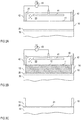
- Figures 2A - 2C illustrate one example of a method according to Figure 1 in greater detail.
- Each of Figures 2A - 2C shows a vertical cross sectional view of one example of a semiconductor wafer, Figures 2A and 2B further show an arrangement used to form a porous region in the semiconductor wafer.
- each of the first and second semiconductor layers 10, 20 is a doped semiconductor layer, wherein at least one of conditions (a) and (b) as outlined above is met with regard to a doping of the first semiconductor layer 10 and a doping of the second semiconductor layer 20.
- a current flows between the first and second electrode 41, 42 via the porosifying agent 50 and the first semiconductor layer 10, wherein the energy associated with this current causes the porosifying agent 50 to porosify the first semiconductor layer 10 in those regions that are in contact with the agent 50.
- the current flowing between the first and second electrodes 41, 42 is associated with a current density at the first surface 11 of the first semiconductor layer 10, wherein the current density in a certain region of the first surface 11 is given by the current flowing into that region divided an area of that region.
- the porosifying agent 50 includes hydrofluoric acid (HF).
- HF hydrofluoric acid
- an aqueous solution including HF is used as the porosifying agent 50.
- the porosifying agent 50 includes HF and ethanol such as an aqueous solution including HF and ethanol.
- the aqueous solution is such that a concentration of HF in the aqueous solution is between 20% and 25%.
- a polarity of the voltage V1 is such that an electrical potential of the first electrode 41 is more negative than an electrical potential of the second electrode 42.
- the second electrode 42 acts as an anode and the first electrode 41 acts as a cathode in the porosification process.
- the porosifying agent 50 forms a porous region 12 in the first semiconductor layer 10.
- the porosification starts at the first surface 11. That is, at first, the porous region 12 is formed at the first surface 11 where the porosifying agent 50, at first, is in contact with the first semiconductor layer 10.
- the porosifying agent 50 penetrates the porous region 12, so that the porous region 12 further extends into the first semiconductor layer 10.
- Figure 2B shows the porous region 12 formed by the porosification process.
- the porous region 12 in a vertical direction, extends from the first surface 11 of the semiconductor layer 10 through the first semiconductor layer 10 down to the second semiconductor layer 20.
- the porous region 12 may extend to the second semiconductor layer 20, but not into the second semiconductor layer 20. That is, the second semiconductor layer 20 may essentially remain unaffected by the porosification process.
- This can be achieved by implementing the first semiconductor layer 10 with a higher doping concentration than the second semiconductor layer 20 and/or with a doping type that is complementary to a doping type of the first semiconductor layer 10, as mentioned above.
- the first semiconductor layer 10 is a p-type (p-doped) layer and the second semiconductor layer 20 is an n-type (n-doped) layer.
- the reservoir accommodating the porosifying agent 50 is formed on top of the first surface 11 such that the porosifying agent 50, at the beginning of the porosification process is in contact with at least 80%, at least 90%, or at least 95% of the first surface 11 of the first semiconductor layer 10.
- the rim 13 is less than 20%, less than 10% or less than 5% of the first semiconductor layer 10.
- the second semiconductor layer 20 is essentially unaffected by the porosification process and the removal process. That is, most of the semiconductor layer 10 is removed down to the second semiconductor layer 20, while the second semiconductor layer 20 is essentially not removed.
- the thickness of the removed material is essentially given by the thickness of the first semiconductor layer 10, while the thickness of the second semiconductor layer 20 is essentially maintained.
- a first surface 21 of the second semiconductor layer 20 that is obtained by the removal process is essentially defined by an interface between the first semiconductor layer 10 and the second semiconductor layer 20 before the porosification process. In other words, the porosification and removal process essentially stops at this interface. This is independent of possible thickness variations of the first semiconductor layer, that is, independent of whether the surface 11 of the first layer 10 is planar or non-planar.
- the etching process can be a dry etching process such as a plasma etching process using at least one of Cl 2 , SF 6 , HBr, NF 3 , CF 4 or a wet etching process such as an etching process using a solution of HF and HNO 3 , a solution of TMAH (Tetramethylammonium hydroxide) and alcohol, or a solution of KOH and alcohol.
- TMAH Tetramethylammonium hydroxide
- a plurality of identical semiconductor devices have been formed in the second semiconductor layer 20 before partially removing the first semiconductor layer, and the wafer is finally divided up in order to form a plurality of single semiconductor devices.
- semiconductor device includes a discrete semiconductor device such as a transistor, a diode, a thyristor, or the like, but also an integrated circuit with a plurality of devices.
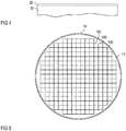
- Figure 5 schematically shows a top view of the wafer after partially removing the first semiconductor layer 10, that is, after the process illustrated in Figures 2A to 2C . More specifically, Figure 5 shows a top view of the rim 13 and of the first surface 21 of the second semiconductor layer 20, wherein this first surface 21 is uncovered by removing the porous region 12.
- reference number 100 schematically illustrates positions of a plurality of individual semiconductor devices. These semiconductor devices are located spaced apart from the edge surface 14 and the rim 13. The wafer is finally divided up along cutting lines located between the individual semiconductor devices in order to obtain a plurality of single semiconductor devices. According to one example, the rim 13 is removed before dividing up the wafer.
- the wafer is divided up without prior removal of the rim 13.
- the rim 13 is "automatically" removed, so that there is no need to remove the rim 13 beforehand.
- FIGs 7A-7B One example of how the porosification process can be improved in order to avoid a situation as illustrated in Figure 6 is illustrated in Figures 7A-7B .
- This example includes implementing the first semiconductor layer 10 such that a thickness of the first semiconductor layer 10 has a minimum in the center of the wafer and increases towards the edge surface 13.
- the first surface 11 is conical (as illustrated in Figure 7A ), dished (not shown) or the like.
- Figure 7A shows the wafer during the porosification process.
- a first surface 11 of this type can be obtained by a polishing or grinding process, for example.
- the porosification starts at the first surface 11 below the first electrode 41, and the porous region 12 extends from those sections of the first surface 11 that are located below the first electrode 41 in the vertical direction and in horizontal directions.
- the porous region 12 touches the second semiconductor layer 20 in the center of the wafer first, as illustrated in Figure 7A . From there, the porous region 12 further expands in horizontal directions until substantially the first semiconductor layer 10 is completely porosified below those sections of the first surface 11 that are in contact with the porosifying agent 50.
- the first electrode 41 has the form of a plate.
- the porosification process is improved by modifying the geometry of the first semiconductor layer 10.
- an improved porosification process can be achieved by suitably adjusting the current density at the first surface 11 during the porosification process.
- suitably adjusting the current density at the first surface 11 includes adjusting the current density such that the current density along the first surface 11, at least in sections, decreases between a center of the first semiconductor layer 10 and an edge region where the first semiconductor layer 10 is connected to the second electrode 42. "This is referred to a as lateral variation of the current density" in the following.
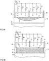
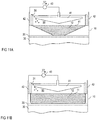
- FIG 8A shows the wafer during the porosification process.
- the porous region 12 starts to the formed below the first electrode 41 at the surface 11 of the first semiconductor layer 10 and, from there, expands in the vertical direction and in horizontal directions.
- porous region 12 touches the second semiconductor layer 20 in the center of the wafer first and, from there, further expands in horizontal directions.
- Figures 9A and 9B illustrate another example of a porosification process in which the current density decreases towards the edge region.
- the first electrode 41 has a plurality of electrode sections 41 1 -41 7 wherein a distance between these electrode sections 41 1 -41 7 and the first surface 11 increases as the distance of the respective electrode section to the center of the wafer increases.
- the more distant an electrode section 41 1 -41 7 is located from the center of the wafer in horizontal directions, the more distant the respective electrode section is located from the first surface 11 in the vertical direction and the lower is a current density at the first surface 11.
- the porosifying agent forms a resistor between the first electrode 41 and the first surface 11.
- the more distant a section of the electrode 41 is from the first surface 11, the higher is a resistance between the respective section of the first electrode 41 and the first surface 11, and the lower is the current density at the first surface 11 below the respective section of the first electrode 41).
- first electrode 41 of the type illustrated in Figure 10B connecting each of the rings 41 A -41 C to the voltage or current source 43 via a respective electronic switch 44 A -44 C , and activating (switching on) the switches 44 A -44 C successively such that at the beginning of the porosification process an innermost ring 41 A is connected to the voltage or current source 43, then the directly adjacent ring 41 B is connected to the voltage or current source 43, and so on.
- the rings 41 A -41 C may have the same distance from the surface 21.
- Figure 11A shows the wafer during the porosification process
- Figure 11B shows the wafer after the porosification process.
- the porous region 12 propagates faster into the first semiconductor layer 10 in the center of the wafer so that the porous region 12 touches the second semiconductor layer 20 in the center of the wafer first.
- Figure 12 illustrates the result of an imperfect porosification process according to another example.
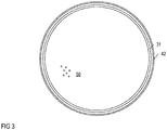
- non-porosified regions (residuals) 16 of the first semiconductor layer 10 remain in a region close to the rim 13, that is, close to the edge surface 14 after the porosification process and the removal process.
- the first semiconductor layer 10 may include one or more of these residuals 16 that are spaced apart from each other or may include one residual 16 that extends along the rim 13 has essentially the form of a ring.
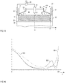
- FIG. 13 One example of a porosification process that is suitable to avoid residuals of the type illustrated in Figure 12 or that is suitable to at least to reduce the size of these residuals 16 is illustrated in Figure 13 .
- This porosification process is based on the porosification process illustrated in Figures 8A and 8B and is different from the porosification process illustrated in Figures 8A and 8B in that the current density in the edge region of the first surface 11 is reduced (as compared to the method according to Figures 8A and 8B ) by increasing a resistance between the first electrode 41 and the first surface 11 in the edge region, wherein increasing the resistance results in a further decrease of the current density in the edge region.
- reducing the active height of the porosifying agent 50 above the edge region of the first semiconductor layer 10 is achieved by providing an electrically insulating element 33 that adjoins the tubular element 31, extends inwardly from the tubular element 31, and is spaced apart from the first surface 11 of the first semiconductor layer 10.
- This element 33 may have the form of a ring in a section plane perpendicular to the section plane shown in Figure 13 .
- the first dimension d33 of the insulating element is between 1 centimeter (cm) and 3 centimeter. According to one example, a maximum distance between the insulating element 33 and the first surface 11 is 1.5 cm, in particular 1cm.
- Curve 203 illustrates the current density in a porosification process in which a ring 33 of the type shown in Figures 14 or 15 has been used. As can be seen from Figure 16 in this example, the current density in the edge region is lower than in the first scenario (see curve 201, no ring), so that the risk that residuals are formed is significantly reduced.
- the second semiconductor layer 20 is used to integrate semiconductor devices therein.
- the doping concentration of the second layer 20 is selected such that a selective porosification can be obtained and that semiconductor devices with desired electric characteristics can be achieved.
- the transistor device shown in Figures 18 and 19 is a vertical transistor device. It should be noted that a transistor device is only one example of a variety of vertical semiconductor devices that can be formed based on the second semiconductor layer 20. Further examples include, but are not restricted to, a vertical diode, a vertical thyristor, or the like.
- a doping concentration of the second semiconductor layer 20 is less than 1E-2 times the doping concentration of the first semiconductor layer in order to achieve a selective porosification process.
- a second semiconductor layer 20 with a doping concentration suitable to achieve a selective porosification process is not suitable for integrating active device regions such as drift regions of vertical transistor cells therein.
- the wafer may further include a third semiconductor layer 30 (illustrated in dashed lines in the drawings) on top of the second semiconductor layer 20, wherein the second semiconductor layer 20 is a thin layer with a thickness of less than 10 micrometers, for example.
Landscapes
- Chemical & Material Sciences (AREA)
- Chemical Kinetics & Catalysis (AREA)
- Engineering & Computer Science (AREA)
- Electrochemistry (AREA)
- Materials Engineering (AREA)
- Metallurgy (AREA)
- Organic Chemistry (AREA)
- Element Separation (AREA)
- General Chemical & Material Sciences (AREA)
- Weting (AREA)
- Metal-Oxide And Bipolar Metal-Oxide Semiconductor Integrated Circuits (AREA)
- Bipolar Transistors (AREA)
Priority Applications (2)
| Application Number | Priority Date | Filing Date | Title |
|---|---|---|---|
| US16/677,801 US11404262B2 (en) | 2018-11-23 | 2019-11-08 | Method for partially removing a semiconductor wafer |
| US17/841,781 US11810779B2 (en) | 2018-11-23 | 2022-06-16 | Method of porosifying part of a semiconductor wafer |
Applications Claiming Priority (1)
| Application Number | Priority Date | Filing Date | Title |
|---|---|---|---|
| DE102018129594.4A DE102018129594B4 (de) | 2018-11-23 | 2018-11-23 | Teilweises entfernen eines halbleiterwafers |
Publications (3)
| Publication Number | Publication Date |
|---|---|
| EP3667706A2 true EP3667706A2 (fr) | 2020-06-17 |
| EP3667706A3 EP3667706A3 (fr) | 2020-11-25 |
| EP3667706B1 EP3667706B1 (fr) | 2024-01-17 |
Family
ID=68295948
Family Applications (1)
| Application Number | Title | Priority Date | Filing Date |
|---|---|---|---|
| EP19202851.2A Active EP3667706B1 (fr) | 2018-11-23 | 2019-10-11 | Élimination partielle d'une tranche de semiconducteur |
Country Status (3)
| Country | Link |
|---|---|
| US (2) | US11404262B2 (fr) |
| EP (1) | EP3667706B1 (fr) |
| DE (1) | DE102018129594B4 (fr) |
Families Citing this family (1)
| Publication number | Priority date | Publication date | Assignee | Title |
|---|---|---|---|---|
| DE102018129594B4 (de) * | 2018-11-23 | 2025-09-04 | Infineon Technologies Ag | Teilweises entfernen eines halbleiterwafers |
Family Cites Families (10)
| Publication number | Priority date | Publication date | Assignee | Title |
|---|---|---|---|---|
| US6921467B2 (en) * | 1996-07-15 | 2005-07-26 | Semitool, Inc. | Processing tools, components of processing tools, and method of making and using same for electrochemical processing of microelectronic workpieces |
| US6664169B1 (en) * | 1999-06-08 | 2003-12-16 | Canon Kabushiki Kaisha | Process for producing semiconductor member, process for producing solar cell, and anodizing apparatus |
| DE10161202C1 (de) * | 2001-12-13 | 2003-05-08 | Bosch Gmbh Robert | Verfahren zur Reduktion der Dicke eines Silizium-Substrates |
| DE10345447B4 (de) * | 2003-09-30 | 2007-04-26 | Infineon Technologies Ag | Verfahren zum Herstellen eines Halbleiter-Bauteils |
| US20060046499A1 (en) * | 2004-08-20 | 2006-03-02 | Dolechek Kert L | Apparatus for use in thinning a semiconductor workpiece |
| EP1881890A2 (fr) * | 2005-05-18 | 2008-01-30 | Matsushita Electric Works, Ltd. | Procede de fabrication d'une lentille optique |
| US9624597B2 (en) * | 2013-06-13 | 2017-04-18 | Yan Ye | Methods and apparatuses for delaminating process pieces |
| US9217206B2 (en) * | 2013-09-27 | 2015-12-22 | Sunpower Corporation | Enhanced porosification |
| WO2015120424A1 (fr) * | 2014-02-10 | 2015-08-13 | Rensselaer Polytechnic Institute | Gravure électrochimique sélective d'un semi-conducteur |
| DE102018129594B4 (de) * | 2018-11-23 | 2025-09-04 | Infineon Technologies Ag | Teilweises entfernen eines halbleiterwafers |
-
2018
- 2018-11-23 DE DE102018129594.4A patent/DE102018129594B4/de active Active
-
2019
- 2019-10-11 EP EP19202851.2A patent/EP3667706B1/fr active Active
- 2019-11-08 US US16/677,801 patent/US11404262B2/en active Active
-
2022
- 2022-06-16 US US17/841,781 patent/US11810779B2/en active Active
Also Published As
| Publication number | Publication date |
|---|---|
| EP3667706A3 (fr) | 2020-11-25 |
| US11404262B2 (en) | 2022-08-02 |
| US20200168449A1 (en) | 2020-05-28 |
| US20220310380A1 (en) | 2022-09-29 |
| EP3667706B1 (fr) | 2024-01-17 |
| DE102018129594A1 (de) | 2020-05-28 |
| US11810779B2 (en) | 2023-11-07 |
| DE102018129594B4 (de) | 2025-09-04 |
Similar Documents
| Publication | Publication Date | Title |
|---|---|---|
| CN109698230B (zh) | 具有dV/dt可控性的IGBT | |
| CN109698197B (zh) | 用于产生具有dV/dt可控性的IGBT的方法 | |
| US9396997B2 (en) | Method for producing a semiconductor component with insulated semiconductor mesas | |
| US9219143B2 (en) | Semiconductor device and super junction semiconductor device having semiconductor mesas | |
| CN103996701B (zh) | 一种超结半导体器件及其制造方法 | |
| CN104465734B (zh) | 绝缘栅双极型晶体管及其制造方法 | |
| US10410911B2 (en) | Buried insulator regions and methods of formation thereof | |
| KR101955055B1 (ko) | 전력용 반도체 소자 및 그 소자의 제조 방법 | |
| JP2010045245A (ja) | 半導体装置および半導体装置の製造方法 | |
| US9496337B2 (en) | Method for producing a semiconductor device having a beveled edge termination | |
| CN108389787A (zh) | 半导体器件及其制造方法 | |
| US11227945B2 (en) | Transistor having at least one transistor cell with a field electrode | |
| CN107039502A (zh) | 形成半导体器件的方法以及半导体器件 | |
| US11810779B2 (en) | Method of porosifying part of a semiconductor wafer | |
| CN104347475B (zh) | 具有沟槽隔离区的边缘终止结构 | |
| US9472395B2 (en) | Semiconductor arrangement including buried anodic oxide and manufacturing method | |
| US7956419B2 (en) | Trench IGBT with depletion stop layer | |
| EP3511988B1 (fr) | Dispositif électronique à semiconducteur avec grille à tranchée et son procédé de fabrication | |
| US9178013B2 (en) | Semiconductor device with edge termination and method for manufacturing a semiconductor device | |
| US10608099B2 (en) | Methods of manufacturing semiconductor devices with a deep barrier layer |
Legal Events
| Date | Code | Title | Description |
|---|---|---|---|
| PUAI | Public reference made under article 153(3) epc to a published international application that has entered the european phase |
Free format text: ORIGINAL CODE: 0009012 |
|
| STAA | Information on the status of an ep patent application or granted ep patent |
Free format text: STATUS: THE APPLICATION HAS BEEN PUBLISHED |
|
| AK | Designated contracting states |
Kind code of ref document: A2 Designated state(s): AL AT BE BG CH CY CZ DE DK EE ES FI FR GB GR HR HU IE IS IT LI LT LU LV MC MK MT NL NO PL PT RO RS SE SI SK SM TR |
|
| AX | Request for extension of the european patent |
Extension state: BA ME |
|
| PUAL | Search report despatched |
Free format text: ORIGINAL CODE: 0009013 |
|
| AK | Designated contracting states |
Kind code of ref document: A3 Designated state(s): AL AT BE BG CH CY CZ DE DK EE ES FI FR GB GR HR HU IE IS IT LI LT LU LV MC MK MT NL NO PL PT RO RS SE SI SK SM TR |
|
| AX | Request for extension of the european patent |
Extension state: BA ME |
|
| RIC1 | Information provided on ipc code assigned before grant |
Ipc: H01L 21/3063 20060101AFI20201021BHEP Ipc: H01L 29/66 20060101ALI20201021BHEP Ipc: C25F 3/12 20060101ALI20201021BHEP |
|
| STAA | Information on the status of an ep patent application or granted ep patent |
Free format text: STATUS: REQUEST FOR EXAMINATION WAS MADE |
|
| 17P | Request for examination filed |
Effective date: 20210525 |
|
| RBV | Designated contracting states (corrected) |
Designated state(s): AL AT BE BG CH CY CZ DE DK EE ES FI FR GB GR HR HU IE IS IT LI LT LU LV MC MK MT NL NO PL PT RO RS SE SI SK SM TR |
|
| GRAP | Despatch of communication of intention to grant a patent |
Free format text: ORIGINAL CODE: EPIDOSNIGR1 |
|
| STAA | Information on the status of an ep patent application or granted ep patent |
Free format text: STATUS: GRANT OF PATENT IS INTENDED |
|
| RIC1 | Information provided on ipc code assigned before grant |
Ipc: C25F 3/12 20060101ALI20230710BHEP Ipc: H01L 29/66 20060101ALI20230710BHEP Ipc: H01L 29/78 20060101ALI20230710BHEP Ipc: H01L 29/739 20060101ALI20230710BHEP Ipc: H01L 29/06 20060101ALI20230710BHEP Ipc: H01L 21/3063 20060101AFI20230710BHEP |
|
| INTG | Intention to grant announced |
Effective date: 20230809 |
|
| P01 | Opt-out of the competence of the unified patent court (upc) registered |
Effective date: 20231011 |
|
| GRAS | Grant fee paid |
Free format text: ORIGINAL CODE: EPIDOSNIGR3 |
|
| GRAA | (expected) grant |
Free format text: ORIGINAL CODE: 0009210 |
|
| STAA | Information on the status of an ep patent application or granted ep patent |
Free format text: STATUS: THE PATENT HAS BEEN GRANTED |
|
| AK | Designated contracting states |
Kind code of ref document: B1 Designated state(s): AL AT BE BG CH CY CZ DE DK EE ES FI FR GB GR HR HU IE IS IT LI LT LU LV MC MK MT NL NO PL PT RO RS SE SI SK SM TR |
|
| REG | Reference to a national code |
Ref country code: GB Ref legal event code: FG4D |
|
| REG | Reference to a national code |
Ref country code: CH Ref legal event code: EP |
|
| REG | Reference to a national code |
Ref country code: DE Ref legal event code: R096 Ref document number: 602019045156 Country of ref document: DE |
|
| REG | Reference to a national code |
Ref country code: IE Ref legal event code: FG4D |
|
| REG | Reference to a national code |
Ref country code: LT Ref legal event code: MG9D |
|
| REG | Reference to a national code |
Ref country code: NL Ref legal event code: MP Effective date: 20240117 |
|
| REG | Reference to a national code |
Ref country code: AT Ref legal event code: MK05 Ref document number: 1651114 Country of ref document: AT Kind code of ref document: T Effective date: 20240117 |
|
| PG25 | Lapsed in a contracting state [announced via postgrant information from national office to epo] |
Ref country code: NL Free format text: LAPSE BECAUSE OF FAILURE TO SUBMIT A TRANSLATION OF THE DESCRIPTION OR TO PAY THE FEE WITHIN THE PRESCRIBED TIME-LIMIT Effective date: 20240117 |
|
| PG25 | Lapsed in a contracting state [announced via postgrant information from national office to epo] |
Ref country code: NL Free format text: LAPSE BECAUSE OF FAILURE TO SUBMIT A TRANSLATION OF THE DESCRIPTION OR TO PAY THE FEE WITHIN THE PRESCRIBED TIME-LIMIT Effective date: 20240117 |
|
| PG25 | Lapsed in a contracting state [announced via postgrant information from national office to epo] |
Ref country code: IS Free format text: LAPSE BECAUSE OF FAILURE TO SUBMIT A TRANSLATION OF THE DESCRIPTION OR TO PAY THE FEE WITHIN THE PRESCRIBED TIME-LIMIT Effective date: 20240517 |
|
| PG25 | Lapsed in a contracting state [announced via postgrant information from national office to epo] |
Ref country code: LT Free format text: LAPSE BECAUSE OF FAILURE TO SUBMIT A TRANSLATION OF THE DESCRIPTION OR TO PAY THE FEE WITHIN THE PRESCRIBED TIME-LIMIT Effective date: 20240117 |
|
| PG25 | Lapsed in a contracting state [announced via postgrant information from national office to epo] |
Ref country code: GR Free format text: LAPSE BECAUSE OF FAILURE TO SUBMIT A TRANSLATION OF THE DESCRIPTION OR TO PAY THE FEE WITHIN THE PRESCRIBED TIME-LIMIT Effective date: 20240418 |
|
| PG25 | Lapsed in a contracting state [announced via postgrant information from national office to epo] |
Ref country code: RS Free format text: LAPSE BECAUSE OF FAILURE TO SUBMIT A TRANSLATION OF THE DESCRIPTION OR TO PAY THE FEE WITHIN THE PRESCRIBED TIME-LIMIT Effective date: 20240417 Ref country code: HR Free format text: LAPSE BECAUSE OF FAILURE TO SUBMIT A TRANSLATION OF THE DESCRIPTION OR TO PAY THE FEE WITHIN THE PRESCRIBED TIME-LIMIT Effective date: 20240117 |
|
| PG25 | Lapsed in a contracting state [announced via postgrant information from national office to epo] |
Ref country code: ES Free format text: LAPSE BECAUSE OF FAILURE TO SUBMIT A TRANSLATION OF THE DESCRIPTION OR TO PAY THE FEE WITHIN THE PRESCRIBED TIME-LIMIT Effective date: 20240117 |
|
| PG25 | Lapsed in a contracting state [announced via postgrant information from national office to epo] |
Ref country code: AT Free format text: LAPSE BECAUSE OF FAILURE TO SUBMIT A TRANSLATION OF THE DESCRIPTION OR TO PAY THE FEE WITHIN THE PRESCRIBED TIME-LIMIT Effective date: 20240117 |
|
| PG25 | Lapsed in a contracting state [announced via postgrant information from national office to epo] |
Ref country code: RS Free format text: LAPSE BECAUSE OF FAILURE TO SUBMIT A TRANSLATION OF THE DESCRIPTION OR TO PAY THE FEE WITHIN THE PRESCRIBED TIME-LIMIT Effective date: 20240417 Ref country code: NO Free format text: LAPSE BECAUSE OF FAILURE TO SUBMIT A TRANSLATION OF THE DESCRIPTION OR TO PAY THE FEE WITHIN THE PRESCRIBED TIME-LIMIT Effective date: 20240417 Ref country code: LT Free format text: LAPSE BECAUSE OF FAILURE TO SUBMIT A TRANSLATION OF THE DESCRIPTION OR TO PAY THE FEE WITHIN THE PRESCRIBED TIME-LIMIT Effective date: 20240117 Ref country code: IS Free format text: LAPSE BECAUSE OF FAILURE TO SUBMIT A TRANSLATION OF THE DESCRIPTION OR TO PAY THE FEE WITHIN THE PRESCRIBED TIME-LIMIT Effective date: 20240517 Ref country code: HR Free format text: LAPSE BECAUSE OF FAILURE TO SUBMIT A TRANSLATION OF THE DESCRIPTION OR TO PAY THE FEE WITHIN THE PRESCRIBED TIME-LIMIT Effective date: 20240117 Ref country code: GR Free format text: LAPSE BECAUSE OF FAILURE TO SUBMIT A TRANSLATION OF THE DESCRIPTION OR TO PAY THE FEE WITHIN THE PRESCRIBED TIME-LIMIT Effective date: 20240418 Ref country code: FI Free format text: LAPSE BECAUSE OF FAILURE TO SUBMIT A TRANSLATION OF THE DESCRIPTION OR TO PAY THE FEE WITHIN THE PRESCRIBED TIME-LIMIT Effective date: 20240117 Ref country code: ES Free format text: LAPSE BECAUSE OF FAILURE TO SUBMIT A TRANSLATION OF THE DESCRIPTION OR TO PAY THE FEE WITHIN THE PRESCRIBED TIME-LIMIT Effective date: 20240117 Ref country code: BG Free format text: LAPSE BECAUSE OF FAILURE TO SUBMIT A TRANSLATION OF THE DESCRIPTION OR TO PAY THE FEE WITHIN THE PRESCRIBED TIME-LIMIT Effective date: 20240117 Ref country code: AT Free format text: LAPSE BECAUSE OF FAILURE TO SUBMIT A TRANSLATION OF THE DESCRIPTION OR TO PAY THE FEE WITHIN THE PRESCRIBED TIME-LIMIT Effective date: 20240117 |
|
| PG25 | Lapsed in a contracting state [announced via postgrant information from national office to epo] |
Ref country code: PL Free format text: LAPSE BECAUSE OF FAILURE TO SUBMIT A TRANSLATION OF THE DESCRIPTION OR TO PAY THE FEE WITHIN THE PRESCRIBED TIME-LIMIT Effective date: 20240117 Ref country code: PT Free format text: LAPSE BECAUSE OF FAILURE TO SUBMIT A TRANSLATION OF THE DESCRIPTION OR TO PAY THE FEE WITHIN THE PRESCRIBED TIME-LIMIT Effective date: 20240517 |
|
| PG25 | Lapsed in a contracting state [announced via postgrant information from national office to epo] |
Ref country code: SE Free format text: LAPSE BECAUSE OF FAILURE TO SUBMIT A TRANSLATION OF THE DESCRIPTION OR TO PAY THE FEE WITHIN THE PRESCRIBED TIME-LIMIT Effective date: 20240117 Ref country code: PT Free format text: LAPSE BECAUSE OF FAILURE TO SUBMIT A TRANSLATION OF THE DESCRIPTION OR TO PAY THE FEE WITHIN THE PRESCRIBED TIME-LIMIT Effective date: 20240517 Ref country code: PL Free format text: LAPSE BECAUSE OF FAILURE TO SUBMIT A TRANSLATION OF THE DESCRIPTION OR TO PAY THE FEE WITHIN THE PRESCRIBED TIME-LIMIT Effective date: 20240117 Ref country code: LV Free format text: LAPSE BECAUSE OF FAILURE TO SUBMIT A TRANSLATION OF THE DESCRIPTION OR TO PAY THE FEE WITHIN THE PRESCRIBED TIME-LIMIT Effective date: 20240117 |
|
| PG25 | Lapsed in a contracting state [announced via postgrant information from national office to epo] |
Ref country code: DK Free format text: LAPSE BECAUSE OF FAILURE TO SUBMIT A TRANSLATION OF THE DESCRIPTION OR TO PAY THE FEE WITHIN THE PRESCRIBED TIME-LIMIT Effective date: 20240117 |
|
| PG25 | Lapsed in a contracting state [announced via postgrant information from national office to epo] |
Ref country code: SM Free format text: LAPSE BECAUSE OF FAILURE TO SUBMIT A TRANSLATION OF THE DESCRIPTION OR TO PAY THE FEE WITHIN THE PRESCRIBED TIME-LIMIT Effective date: 20240117 |
|
| REG | Reference to a national code |
Ref country code: DE Ref legal event code: R097 Ref document number: 602019045156 Country of ref document: DE |
|
| PG25 | Lapsed in a contracting state [announced via postgrant information from national office to epo] |
Ref country code: EE Free format text: LAPSE BECAUSE OF FAILURE TO SUBMIT A TRANSLATION OF THE DESCRIPTION OR TO PAY THE FEE WITHIN THE PRESCRIBED TIME-LIMIT Effective date: 20240117 Ref country code: CZ Free format text: LAPSE BECAUSE OF FAILURE TO SUBMIT A TRANSLATION OF THE DESCRIPTION OR TO PAY THE FEE WITHIN THE PRESCRIBED TIME-LIMIT Effective date: 20240117 |
|
| PG25 | Lapsed in a contracting state [announced via postgrant information from national office to epo] |
Ref country code: SK Free format text: LAPSE BECAUSE OF FAILURE TO SUBMIT A TRANSLATION OF THE DESCRIPTION OR TO PAY THE FEE WITHIN THE PRESCRIBED TIME-LIMIT Effective date: 20240117 |
|
| PG25 | Lapsed in a contracting state [announced via postgrant information from national office to epo] |
Ref country code: SM Free format text: LAPSE BECAUSE OF FAILURE TO SUBMIT A TRANSLATION OF THE DESCRIPTION OR TO PAY THE FEE WITHIN THE PRESCRIBED TIME-LIMIT Effective date: 20240117 Ref country code: SK Free format text: LAPSE BECAUSE OF FAILURE TO SUBMIT A TRANSLATION OF THE DESCRIPTION OR TO PAY THE FEE WITHIN THE PRESCRIBED TIME-LIMIT Effective date: 20240117 Ref country code: RO Free format text: LAPSE BECAUSE OF FAILURE TO SUBMIT A TRANSLATION OF THE DESCRIPTION OR TO PAY THE FEE WITHIN THE PRESCRIBED TIME-LIMIT Effective date: 20240117 Ref country code: EE Free format text: LAPSE BECAUSE OF FAILURE TO SUBMIT A TRANSLATION OF THE DESCRIPTION OR TO PAY THE FEE WITHIN THE PRESCRIBED TIME-LIMIT Effective date: 20240117 Ref country code: DK Free format text: LAPSE BECAUSE OF FAILURE TO SUBMIT A TRANSLATION OF THE DESCRIPTION OR TO PAY THE FEE WITHIN THE PRESCRIBED TIME-LIMIT Effective date: 20240117 Ref country code: CZ Free format text: LAPSE BECAUSE OF FAILURE TO SUBMIT A TRANSLATION OF THE DESCRIPTION OR TO PAY THE FEE WITHIN THE PRESCRIBED TIME-LIMIT Effective date: 20240117 |
|
| PLBE | No opposition filed within time limit |
Free format text: ORIGINAL CODE: 0009261 |
|
| STAA | Information on the status of an ep patent application or granted ep patent |
Free format text: STATUS: NO OPPOSITION FILED WITHIN TIME LIMIT |
|
| PG25 | Lapsed in a contracting state [announced via postgrant information from national office to epo] |
Ref country code: IT Free format text: LAPSE BECAUSE OF FAILURE TO SUBMIT A TRANSLATION OF THE DESCRIPTION OR TO PAY THE FEE WITHIN THE PRESCRIBED TIME-LIMIT Effective date: 20240117 |
|
| 26N | No opposition filed |
Effective date: 20241018 |
|
| PG25 | Lapsed in a contracting state [announced via postgrant information from national office to epo] |
Ref country code: IT Free format text: LAPSE BECAUSE OF FAILURE TO SUBMIT A TRANSLATION OF THE DESCRIPTION OR TO PAY THE FEE WITHIN THE PRESCRIBED TIME-LIMIT Effective date: 20240117 |
|
| PG25 | Lapsed in a contracting state [announced via postgrant information from national office to epo] |
Ref country code: SI Free format text: LAPSE BECAUSE OF FAILURE TO SUBMIT A TRANSLATION OF THE DESCRIPTION OR TO PAY THE FEE WITHIN THE PRESCRIBED TIME-LIMIT Effective date: 20240117 |
|
| REG | Reference to a national code |
Ref country code: CH Ref legal event code: PL |
|
| GBPC | Gb: european patent ceased through non-payment of renewal fee |
Effective date: 20241011 |
|
| PG25 | Lapsed in a contracting state [announced via postgrant information from national office to epo] |
Ref country code: MC Free format text: LAPSE BECAUSE OF FAILURE TO SUBMIT A TRANSLATION OF THE DESCRIPTION OR TO PAY THE FEE WITHIN THE PRESCRIBED TIME-LIMIT Effective date: 20240117 |
|
| PG25 | Lapsed in a contracting state [announced via postgrant information from national office to epo] |
Ref country code: GB Free format text: LAPSE BECAUSE OF NON-PAYMENT OF DUE FEES Effective date: 20241011 |
|
| PG25 | Lapsed in a contracting state [announced via postgrant information from national office to epo] |
Ref country code: LU Free format text: LAPSE BECAUSE OF NON-PAYMENT OF DUE FEES Effective date: 20241011 Ref country code: BE Free format text: LAPSE BECAUSE OF NON-PAYMENT OF DUE FEES Effective date: 20241031 |
|
| PG25 | Lapsed in a contracting state [announced via postgrant information from national office to epo] |
Ref country code: FR Free format text: LAPSE BECAUSE OF NON-PAYMENT OF DUE FEES Effective date: 20241031 |
|
| PG25 | Lapsed in a contracting state [announced via postgrant information from national office to epo] |
Ref country code: CH Free format text: LAPSE BECAUSE OF NON-PAYMENT OF DUE FEES Effective date: 20241031 |
|
| REG | Reference to a national code |
Ref country code: BE Ref legal event code: MM Effective date: 20241031 |
|
| PG25 | Lapsed in a contracting state [announced via postgrant information from national office to epo] |
Ref country code: IE Free format text: LAPSE BECAUSE OF NON-PAYMENT OF DUE FEES Effective date: 20241011 |
|
| REG | Reference to a national code |
Ref country code: DE Ref legal event code: R079 Ref document number: 602019045156 Country of ref document: DE Free format text: PREVIOUS MAIN CLASS: H01L0021306300 Ipc: H10P0050640000 |
|
| PGFP | Annual fee paid to national office [announced via postgrant information from national office to epo] |
Ref country code: DE Payment date: 20251217 Year of fee payment: 7 |
|
| PG25 | Lapsed in a contracting state [announced via postgrant information from national office to epo] |
Ref country code: CY Free format text: LAPSE BECAUSE OF FAILURE TO SUBMIT A TRANSLATION OF THE DESCRIPTION OR TO PAY THE FEE WITHIN THE PRESCRIBED TIME-LIMIT; INVALID AB INITIO Effective date: 20191011 |
|
| PG25 | Lapsed in a contracting state [announced via postgrant information from national office to epo] |
Ref country code: HU Free format text: LAPSE BECAUSE OF FAILURE TO SUBMIT A TRANSLATION OF THE DESCRIPTION OR TO PAY THE FEE WITHIN THE PRESCRIBED TIME-LIMIT; INVALID AB INITIO Effective date: 20191011 |