EP3667721A1 - Procédé de fabrication d'un dispositif optique - Google Patents
Procédé de fabrication d'un dispositif optique Download PDFInfo
- Publication number
- EP3667721A1 EP3667721A1 EP18211315.9A EP18211315A EP3667721A1 EP 3667721 A1 EP3667721 A1 EP 3667721A1 EP 18211315 A EP18211315 A EP 18211315A EP 3667721 A1 EP3667721 A1 EP 3667721A1
- Authority
- EP
- European Patent Office
- Prior art keywords
- leds
- pds
- contact
- array
- led
- Prior art date
- Legal status (The legal status is an assumption and is not a legal conclusion. Google has not performed a legal analysis and makes no representation as to the accuracy of the status listed.)
- Pending
Links
Images


Classifications
-
- H—ELECTRICITY
- H10—SEMICONDUCTOR DEVICES; ELECTRIC SOLID-STATE DEVICES NOT OTHERWISE PROVIDED FOR
- H10H—INORGANIC LIGHT-EMITTING SEMICONDUCTOR DEVICES HAVING POTENTIAL BARRIERS
- H10H29/00—Integrated devices, or assemblies of multiple devices, comprising at least one light-emitting semiconductor element covered by group H10H20/00
- H10H29/10—Integrated devices comprising at least one light-emitting semiconductor component covered by group H10H20/00
- H10H29/14—Integrated devices comprising at least one light-emitting semiconductor component covered by group H10H20/00 comprising multiple light-emitting semiconductor components
-
- H—ELECTRICITY
- H10—SEMICONDUCTOR DEVICES; ELECTRIC SOLID-STATE DEVICES NOT OTHERWISE PROVIDED FOR
- H10H—INORGANIC LIGHT-EMITTING SEMICONDUCTOR DEVICES HAVING POTENTIAL BARRIERS
- H10H20/00—Individual inorganic light-emitting semiconductor devices having potential barriers, e.g. light-emitting diodes [LED]
- H10H20/01—Manufacture or treatment
-
- H—ELECTRICITY
- H10—SEMICONDUCTOR DEVICES; ELECTRIC SOLID-STATE DEVICES NOT OTHERWISE PROVIDED FOR
- H10F—INORGANIC SEMICONDUCTOR DEVICES SENSITIVE TO INFRARED RADIATION, LIGHT, ELECTROMAGNETIC RADIATION OF SHORTER WAVELENGTH OR CORPUSCULAR RADIATION
- H10F39/00—Integrated devices, or assemblies of multiple devices, comprising at least one element covered by group H10F30/00, e.g. radiation detectors comprising photodiode arrays
- H10F39/011—Manufacture or treatment of image sensors covered by group H10F39/12
- H10F39/018—Manufacture or treatment of image sensors covered by group H10F39/12 of hybrid image sensors
-
- H—ELECTRICITY
- H10—SEMICONDUCTOR DEVICES; ELECTRIC SOLID-STATE DEVICES NOT OTHERWISE PROVIDED FOR
- H10F—INORGANIC SEMICONDUCTOR DEVICES SENSITIVE TO INFRARED RADIATION, LIGHT, ELECTROMAGNETIC RADIATION OF SHORTER WAVELENGTH OR CORPUSCULAR RADIATION
- H10F39/00—Integrated devices, or assemblies of multiple devices, comprising at least one element covered by group H10F30/00, e.g. radiation detectors comprising photodiode arrays
- H10F39/011—Manufacture or treatment of image sensors covered by group H10F39/12
- H10F39/026—Wafer-level processing
-
- H—ELECTRICITY
- H10—SEMICONDUCTOR DEVICES; ELECTRIC SOLID-STATE DEVICES NOT OTHERWISE PROVIDED FOR
- H10F—INORGANIC SEMICONDUCTOR DEVICES SENSITIVE TO INFRARED RADIATION, LIGHT, ELECTROMAGNETIC RADIATION OF SHORTER WAVELENGTH OR CORPUSCULAR RADIATION
- H10F39/00—Integrated devices, or assemblies of multiple devices, comprising at least one element covered by group H10F30/00, e.g. radiation detectors comprising photodiode arrays
- H10F39/011—Manufacture or treatment of image sensors covered by group H10F39/12
- H10F39/028—Manufacture or treatment of image sensors covered by group H10F39/12 performed after manufacture of the image sensors, e.g. annealing, gettering of impurities, short-circuit elimination or recrystallisation
-
- H—ELECTRICITY
- H10—SEMICONDUCTOR DEVICES; ELECTRIC SOLID-STATE DEVICES NOT OTHERWISE PROVIDED FOR
- H10F—INORGANIC SEMICONDUCTOR DEVICES SENSITIVE TO INFRARED RADIATION, LIGHT, ELECTROMAGNETIC RADIATION OF SHORTER WAVELENGTH OR CORPUSCULAR RADIATION
- H10F39/00—Integrated devices, or assemblies of multiple devices, comprising at least one element covered by group H10F30/00, e.g. radiation detectors comprising photodiode arrays
- H10F39/10—Integrated devices
- H10F39/12—Image sensors
- H10F39/18—Complementary metal-oxide-semiconductor [CMOS] image sensors; Photodiode array image sensors
-
- H—ELECTRICITY
- H10—SEMICONDUCTOR DEVICES; ELECTRIC SOLID-STATE DEVICES NOT OTHERWISE PROVIDED FOR
- H10F—INORGANIC SEMICONDUCTOR DEVICES SENSITIVE TO INFRARED RADIATION, LIGHT, ELECTROMAGNETIC RADIATION OF SHORTER WAVELENGTH OR CORPUSCULAR RADIATION
- H10F39/00—Integrated devices, or assemblies of multiple devices, comprising at least one element covered by group H10F30/00, e.g. radiation detectors comprising photodiode arrays
- H10F39/80—Constructional details of image sensors
- H10F39/809—Constructional details of image sensors of hybrid image sensors
-
- H—ELECTRICITY
- H10—SEMICONDUCTOR DEVICES; ELECTRIC SOLID-STATE DEVICES NOT OTHERWISE PROVIDED FOR
- H10F—INORGANIC SEMICONDUCTOR DEVICES SENSITIVE TO INFRARED RADIATION, LIGHT, ELECTROMAGNETIC RADIATION OF SHORTER WAVELENGTH OR CORPUSCULAR RADIATION
- H10F39/00—Integrated devices, or assemblies of multiple devices, comprising at least one element covered by group H10F30/00, e.g. radiation detectors comprising photodiode arrays
- H10F39/80—Constructional details of image sensors
- H10F39/811—Interconnections
-
- H—ELECTRICITY
- H10—SEMICONDUCTOR DEVICES; ELECTRIC SOLID-STATE DEVICES NOT OTHERWISE PROVIDED FOR
- H10H—INORGANIC LIGHT-EMITTING SEMICONDUCTOR DEVICES HAVING POTENTIAL BARRIERS
- H10H20/00—Individual inorganic light-emitting semiconductor devices having potential barriers, e.g. light-emitting diodes [LED]
- H10H20/80—Constructional details
- H10H20/81—Bodies
- H10H20/811—Bodies having quantum effect structures or superlattices, e.g. tunnel junctions
- H10H20/812—Bodies having quantum effect structures or superlattices, e.g. tunnel junctions within the light-emitting regions, e.g. having quantum confinement structures
-
- H—ELECTRICITY
- H10—SEMICONDUCTOR DEVICES; ELECTRIC SOLID-STATE DEVICES NOT OTHERWISE PROVIDED FOR
- H10H—INORGANIC LIGHT-EMITTING SEMICONDUCTOR DEVICES HAVING POTENTIAL BARRIERS
- H10H20/00—Individual inorganic light-emitting semiconductor devices having potential barriers, e.g. light-emitting diodes [LED]
- H10H20/80—Constructional details
- H10H20/85—Packages
-
- H—ELECTRICITY
- H10—SEMICONDUCTOR DEVICES; ELECTRIC SOLID-STATE DEVICES NOT OTHERWISE PROVIDED FOR
- H10H—INORGANIC LIGHT-EMITTING SEMICONDUCTOR DEVICES HAVING POTENTIAL BARRIERS
- H10H20/00—Individual inorganic light-emitting semiconductor devices having potential barriers, e.g. light-emitting diodes [LED]
- H10H20/80—Constructional details
- H10H20/85—Packages
- H10H20/857—Interconnections, e.g. lead-frames, bond wires or solder balls
-
- H—ELECTRICITY
- H10—SEMICONDUCTOR DEVICES; ELECTRIC SOLID-STATE DEVICES NOT OTHERWISE PROVIDED FOR
- H10W—GENERIC PACKAGES, INTERCONNECTIONS, CONNECTORS OR OTHER CONSTRUCTIONAL DETAILS OF DEVICES COVERED BY CLASS H10
- H10W90/00—Package configurations
-
- H—ELECTRICITY
- H10—SEMICONDUCTOR DEVICES; ELECTRIC SOLID-STATE DEVICES NOT OTHERWISE PROVIDED FOR
- H10H—INORGANIC LIGHT-EMITTING SEMICONDUCTOR DEVICES HAVING POTENTIAL BARRIERS
- H10H20/00—Individual inorganic light-emitting semiconductor devices having potential barriers, e.g. light-emitting diodes [LED]
- H10H20/01—Manufacture or treatment
- H10H20/011—Manufacture or treatment of bodies, e.g. forming semiconductor layers
- H10H20/018—Bonding of wafers
-
- H—ELECTRICITY
- H10—SEMICONDUCTOR DEVICES; ELECTRIC SOLID-STATE DEVICES NOT OTHERWISE PROVIDED FOR
- H10H—INORGANIC LIGHT-EMITTING SEMICONDUCTOR DEVICES HAVING POTENTIAL BARRIERS
- H10H20/00—Individual inorganic light-emitting semiconductor devices having potential barriers, e.g. light-emitting diodes [LED]
- H10H20/01—Manufacture or treatment
- H10H20/036—Manufacture or treatment of packages
-
- H—ELECTRICITY
- H10—SEMICONDUCTOR DEVICES; ELECTRIC SOLID-STATE DEVICES NOT OTHERWISE PROVIDED FOR
- H10H—INORGANIC LIGHT-EMITTING SEMICONDUCTOR DEVICES HAVING POTENTIAL BARRIERS
- H10H20/00—Individual inorganic light-emitting semiconductor devices having potential barriers, e.g. light-emitting diodes [LED]
- H10H20/01—Manufacture or treatment
- H10H20/036—Manufacture or treatment of packages
- H10H20/0364—Manufacture or treatment of packages of interconnections
-
- H—ELECTRICITY
- H10—SEMICONDUCTOR DEVICES; ELECTRIC SOLID-STATE DEVICES NOT OTHERWISE PROVIDED FOR
- H10H—INORGANIC LIGHT-EMITTING SEMICONDUCTOR DEVICES HAVING POTENTIAL BARRIERS
- H10H29/00—Integrated devices, or assemblies of multiple devices, comprising at least one light-emitting semiconductor element covered by group H10H20/00
- H10H29/10—Integrated devices comprising at least one light-emitting semiconductor component covered by group H10H20/00
- H10H29/14—Integrated devices comprising at least one light-emitting semiconductor component covered by group H10H20/00 comprising multiple light-emitting semiconductor components
- H10H29/142—Two-dimensional arrangements, e.g. asymmetric LED layout
Definitions
- the present invention relates to the technical field of optical devices.
- the invention specifically proposes a method for fabricating an optical device, and presents the optical device itself.
- the optical device is a light emitting diode (LED) device, in particular a micro-LED ( ⁇ LED) device, or is a photodiode (PD) device, in particular a photodiode-based imager.
- LED light emitting diode
- ⁇ LED micro-LED
- PD photodiode
- the method and optical device, respectively, are specifically applicable for a ⁇ LED display.
- CMOS Complementary Metal-Oxide-Semiconductor
- the main challenge in developing new ⁇ LED devices is how to integrate the very closely spaced LEDs, which are commonly made using a III-V or III-N (e.g. GaN) semiconductor material (epitaxial layer) on a 4"-6" wafer, with a Si-CMOS (active matrix readout) IC, typically made on a 8"-12" wafer. That, is how to achieve the integration with a sufficiently small LED pixel pitch, while not causing too much efficiency drop of the LEDs. Notably, efficiency drops are quite common to scaled LEDs.
- III-V or III-N e.g. GaN
- Si-CMOS active matrix readout
- the EQE of a given scaled LED is a secondary concern, which is directly linked to the aperture or fill factor of the active light emitting area of the LED.
- a scaled III-N or III-V LED has non-radiative recombination at the sidewalls of the MESA edge due to defects, which is severe within the diffusion length of the charge carriers.
- the efficiency drop of such a scaled LED is therefore mostly related to perimeter to area ratio of the LED.
- the active semiconductor area should be as large as possible compared to the size of the LED pixel as a whole, wherein the LED pixel includes also the distance to an adjacent LED. In the following, this is referred to as LED aperture or fill factor.
- embodiments of the present invention aim to improve the fabrication of an optical device, in particular of a LED device suitable for a ⁇ LED display, or of a PD device.
- An objective is thereby to fabricate and provide an optical device with an array having a very small pixel pitch but a high efficiency. In particular, only very little efficiency drop should be experienced when scaling LEDs or PDs.
- the LED device should specifically be a ⁇ LED device with LED pixel pitch of 3 ⁇ m or less. Likewise for a PD device, a PD pixel pitch or 3 ⁇ m or less should be possible.
- the fabrication process for the optical device should further be efficient and should allow achieving high yields. Further, the optical device should overall have a compact size.
- Embodiments of the invention base on the realization that - while several conventional integration options would in principle be available for integrating compound semiconductor LEDs or PDs (front-plane) with a CMOS readout (backplane) - only some integration options are suitable for full wafer monolithic integration, and have thus the capability to achieve the required integration target. Furthermore, not all integration options available for monolithic integration are also suitable for achieving the very small LED or PD pixel pitches needed, for example, for a ⁇ LED display, while at the same time efficiency drops of the LEDs or PDs are avoided or suppressed.
- embodiments of the invention base on the insight that - regardless of the integration method selected for combining compound semiconductor LEDs or PDs with a CMOS readout IC - it should be avoided that vias are present within the LED/PD array (especially not Through Silicon Vias (TSVs) or super-vias) for connecting the LEDs or PDs with the CMOS IC. Having vias outside the array is not a problem.
- the embodiments also take into account that any approach that leads towards a bottom LED contact having a larger size then e.g. the MESA etched quantum well of the LED, would negatively impact the efficiency of the LED.
- any integration method that might allow not to etch the quantum well of a LED, but only the doped injection layers, would be superior in performance at scaled dimensions.
- an embodiment of the invention proposes a method (process flow) that employs wafer-to-wafer (W2W) hybrid bonding to integrate LEDs or PDs with a CMOS IC.
- the method avoids vias in the LED/PD array and realizes a bottom contact that is not larger than a quantum well area of a LED or than the active diode area of a PD.
- the method may be split into a process flow for the LED/PD array, which may be done before the W2W hybrid bonding, and a post-process flow for the LED/PD array, which may be done after the W2W hybrid bonding.
- a first aspect of the invention provides a method for fabricating an optical device, the method comprising: processing an array including a plurality of compound semiconductor LEDs or compound semiconductor PDs on a first semiconductor wafer, processing a plurality of first contacts on the first semiconductor wafer, each first contact being electrically connected to one of the LEDs or PDs, processing a CMOS IC on a second semiconductor wafer, processing a plurality of second contacts electrically connected to the CMOS IC on the second semiconductor wafer, and hybrid bonding the first semiconductor wafer to the second semiconductor wafer such that the plurality of LEDs or PDs are individually connected to the CMOS IC via the first and second contacts.
- the W2W hybrid bonding to bond the first semiconductor wafer to the second wafer, and integrated optical device including an LED/PD array and a CMOS readout can be fabricated with a target resolution of a LED/PD pixel pitch of 3 ⁇ m or even less.
- the two semiconductor wafers can be processed separately, and can then be hybrid bonded to integrate the array and the CMOS readout.
- the first semiconductor wafer may include a carrier substrate (carrier wafer), the array on the carrier wafer, and further layers processed on the carrier wafer and/or array, which result in a bonding surface above the array.
- the processing of the array on the first semiconductor wafer may mean that first a plurality of LEDs or PDs are structured from compound semiconductor LED or PD layers provided on the carrier wafer, and then the bonding surface is obtained, in order to obtain the bond-ready first semiconductor wafer. After bonding the first semiconductor wafer to the second semiconductor wafer, via the bonding surface, the carrier wafer may be removed.
- processing the array does not necessarily mean that no further post-processing can be applied, in order to finalize the array or the individual LEDs or PDs, respectively.
- the array does not have to be processed completely before the hybrid bonding step.
- the array should be processed at least to the extent that at least one contact of the LED or PD including the active areas for each LED or PD are already processed.
- the compound semiconductor LEDs or PDs of the array are LEDs or PDs base on or are made from a compound semiconductor material, in particular from a III-V or II-VI semiconductor material.
- the LEDs may be GaN-based LEDs, e.g. made from GaN and/or AlGaN, or may be LEDs made from AlGaInP.
- the PDs may be InP-based PDs, e.g. made from InP.
- multiple optical devices may be fabricated in parallel, thus, a plurality of LED/PD arrays may be processed on the first semiconductor wafer.
- the processing of the arrays on the first semiconductor wafer may in this case include a step of obtaining a plurality of compound semiconductor stacks, each stack including an LED or PD layer and corresponding to one of the optical devices/arrays, which are reconstituted on a silicon-based carrier wafer.
- the array is processed without any VIA through the array between the plurality of LEDs or PDs.
- the LED/PD pixel pitch can be reduced, while at the same time the LED/PD apertures can be maximized.
- This arrangement of the array in combination with the hybrid bonding leads the way for fabricating e.g. improved ⁇ LED devices with very high target resolution, or imagers with very high resolution.
- the array includes a plurality of LEDs and processing the array on the first semiconductor wafer comprises: growing or transferring LED layers on the first semiconductor wafer, wherein the LED layers include quantum well layers and a highly-doped contact layer on the quantum well layers, and structuring the plurality of LEDs by etching the LED layers, wherein the highly-doped contact layer is etched but the quantum well layers are not etched.
- the LED layers including the active area for each LED may be processed.
- the active area of each LED is defined by the non-etched quantum well layers.
- the etching is referred to as a partial MESA etch, since it is stopped at the quantum well layers after the highly-doped contact layer is etched.
- the partial MESA etch reduces efficiency losses caused by scaling the LEDs. That means, a smaller LED pixel pitch becomes possible.
- the partial MESA etch is in particular feasible in the context of the method of the first aspect.
- each first contact is electrically connected to a different one of the LEDs or PDs from below.
- processing, before the hybrid bonding, the plurality of first contacts on the first semiconductor wafer comprises: processing a plurality of contact layers, each contact layer being applied to the bottom surface of a different one of the LEDs or PDs, and processing a plurality of VIAs, each VIA being electrically connected to one of the contact layers from below and extending from the contact layer to the bonding surface of the first semiconductor wafer.
- the contact layers may be p-contacts or n-contacts.
- a size of each contact layer is equal to or smaller than a size of an active area of the LED or PD, to which it is applied.
- the method further comprises, after the hybrid bonding: processing at least one third contact on the first semiconductor wafer, the at least one third contact being electrically connected to the plurality of LEDs or PDs from above.
- the terms “above” and “below” relate to the orientation of the LEDs or PDs and particularly the light emission/capturing axis/direction of the array.
- “Above” or “top” is the side where the array emits light.
- “Below” or “bottom” is the opposite side. Any element referred to as being “below” the LEDs/PDs or the array does thus not interfere with the emitting/capturing of the light.
- the at least one third contact is transparent for LED light or light to be captured by the PDs and is connected to several or to each of the plurality of LEDs or PDs.
- the third contact may be a common contact of LEDs/PDs of the array, thus simplifying the fabrication process and beneficial for achieving a small pixel pitch.
- the method further comprises, after the hybrid bonding: processing at least one electrical connection element, particularly a VIA, connecting the at least one third contact to the CMOS IC, wherein the electrical connection element is passed by or around the array.
- the at least one electrical connection element is not passed through the array, and does therefore not negatively impact on the LED/PD apertures and thus the pixel pitch.
- the electrical connection element is thus arranged outside of the array. That means, in a top view of the array, the electrical connection element is located next to the array.
- the electrical connection element may either being vertical, but located at a certain distance laterally from the array, or may circle around the array.
- a plurality of electrical connection elements is processed, the plurality of electrical connection elements being arranged with a lower density than the plurality of first contacts and second contacts.
- the higher density of the arrangement of the first and second contacts allows achieving the high pixel resolution in an overall compact optical device.
- the method further comprises, after the hybrid bonding: processing a conductive grid, particularly using a damascene process, electrically connected to the at least one third contact from above.
- the conductive grid may distribute current and heat efficiently in the optical device, particularly to/away from the array.
- the grid may also serve as a diaphragm located above the array, in order to produce a narrow emission angle of a LED device, or may serve to focus light onto the PDs in a PD device.
- the array has a pixel pitch of the plurality of LEDs or PDs between 1-10 ⁇ m, in particular equal to or below 3 ⁇ m.
- the method may fabricate a ⁇ LED device suitable for application in a ⁇ LED display, or a ⁇ PD device suitable as a high-resolution imager.
- a second aspect of the invention provides an optical device, comprising a first semiconductor part comprising: an array including a plurality of compound semiconductor LEDs or compound semiconductor PDs, and a plurality of first contacts, each first contact being electrically connected to one of the LEDs or PDs from below; and comprising a second semiconductor part arranged below the first semiconductor part and comprising: a CMOS IC and a plurality of second contacts electrically connected to the CMOS IC; wherein the first semiconductor part is hybrid bonded to the second semiconductor part, and the plurality of first contacts are directly connected one-by-one to the plurality of second contacts.
- the optical device of the second aspect can the fabricated with the method of the first aspect and its implementation forms. After bonding the first semiconductor wafer to the second semiconductor wafer, post-processing and dicing of the bonded wafers may yield multiple optical devices.
- the optical device of the second aspect may be a ⁇ LED or ⁇ PD device with a very high LED/PD resolution in the array, and is thus well suited to be implemented in e.g. a ⁇ LED display or a high-resolution imager.
- the array comprises no VIA between the plurality of LEDs or PDs.
- the LEDs/PDs apertures in the array can be maximized, i.e. the LED or PD surfaces with respect to the overall array area.
- the optical device further comprises at least one third contact electrically connected to the plurality of LEDs or PDs from above, wherein the at least one third contact is transparent for LED light or light to be captured by the PDs and is connected to several or to each of the plurality of LEDs or PDs.
- the third contact may be a common contact connecting several or even all LEDs or PDs.
- the common contact may be transparent at least for the LED light or to be captured light, optionally it may block other electromagnetic radiation.
- the at least one third contact is electrically connected to the CMOS IC by at least one electrical connection element arranged outside of the array.
- the optical device can be designed very compactly, since no electrical connection element runs through the array, which allows moving the LEDs or PDs closer together without reducing the LED/PD apertures.
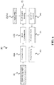
- FIG. 1 shows a method 10 according to an embodiment of the invention in a flow-diagram.
- the method 10 is in particular suitable to obtain an optical device 30 (see FIG. 3 for more details on device 30) e.g. including an array 31, particularly a ⁇ LED or ⁇ PD array.
- the method 10 may, for example, be applied in a fabrication process of a ⁇ LED display including such a LED device as the optical device 30.
- an array 31 including a plurality of compound semiconductor LEDs or compound semiconductor PDs 31a is processed on a first semiconductor wafer.
- a plurality of first contacts 32 is processed on the first semiconductor wafer, each first contact 32 being electrically connected to one of the LEDs or PDs 31a.
- a CMOS IC 33 is processed on a second semiconductor wafer.
- a plurality of second contacts 34 electrically connected to the CMOS IC 33 is processed on the second semiconductor wafer.
- the first semiconductor wafer is hybrid bonded to the second semiconductor wafer such that the plurality of PDs or LEDs 31a are individually connected to the CMOS IC 33 via the first and second contacts 32, 34.
- FIG. 2 shows a method 10 according to an embodiment of the invention, which bases on the method 10 shown in FIG. 1 .
- the method 10 shown in FIG. 2 includes the same steps 11-15 shown in FIG. 1 , and may include additional steps.
- the first semiconductor wafer may be provided with epitaxially grown (epi) LED layers or PD layers, particularly based on a compound semiconductor material.
- a compound semiconductor material stack including each the epi LED/PD layers may be provided on the first semiconductor wafer.
- the epi LED/PD layers may thereby be disposed on a carrier wafer (e.g. for LEDs 31a these may be GaN, AlGaInP or GaN-on-sapphire on a Si carrier wafer, particularly a 300mm wafer; for PDs 31a these may be InP on such a Si carrier wafer).
- the epi LED layers may include layers defining a quantum well (i.e.
- the MESA etch of the epi LED layers may be a full MESA etch, which includes etching through the quantum well layers, or may be a partial MESA etch, which includes only etching through the highly-doped contact layer, but stopping the etch at the quantum well layers. That is, the quantum well layers are not etched, if a partial MESA etch is performed.
- the epi PD layers may include layers defining a PiN diode of a PD 31a.
- the array 31 does not have to be completely finalised in step 11, for instance, regarding contacting, but the LED/PD layers should already be structured into the arrangement of the LEDs or PDs 31a in the array 31.
- the step 12 of processing the plurality of first contacts 32 on the first semiconductor wafer may be divided into two steps 12a and 12b as shown in FIG. 2 .
- a contact layer 32a (see e.g. FIG. 3 ) may be processed onto each LED or PD 31a, particularly referred to as a "bottom contact” due to its arrangement below the LED or PD 31a in the final optical device 30.
- the bottom contact layer 32a can either be a p-contact or n-contact ( FIG. 2 only exemplarily refers to a p-contact, an n-contact is here likewise possible).
- a conventional Back End of Line (BEOL) damascene process e.g.
- VIAs 32b may be used to create VIAs 32b (see e.g. FIG. 3 ), which electrically connect to the plurality of contact layers 32a with one side, and end with their other side at a bonding surface of the first semiconductor wafer. That is, each of these VIAs 32b is electrically connected to one of the contact layers 32a from below, and extends from the contact layer 32a to the bonding surface of the first semiconductor wafer. In particular, the VIAs 32b are exposed at the bonding surface of the first semiconductor wafer.
- the boning surface of the first semiconductor wafer may be a Chemical-Mechanical Planarization (CMP) flat surface with the VIAs 32b functioning as contact regions/pads and an anionic bonding layer (e.g. SiN, SiCN, SiO2).
- CMP Chemical-Mechanical Planarization
- the CMOS IC 33 and the second contacts 34 are processed on the second semiconductor wafer.
- a CMOS wafer containing an active matrix and additional signal processing functions may be provided.
- the second semiconductor wafer is provided with a bonding surface, which may be a CMP flat surface with the second contacts 34 functioning as contact regions/pads and an anionic bonding layer (e.g. SiN, SiCN, SiO2).
- the second contacts 34 are exposed with one of their ends at the bonding surface of the first semiconductor wafer, while their second end connects to the CMOS IC 33.
- the second semiconductor wafer is bonded by (e.g. conventional) W2W hybrid bonding to the first semiconductor wafer.
- a conventional hybrid bonding technique that may be used is, for instance, described in ' SW Kim et al., "Ultra-fine Pitch 3D Integration Using Face-to-Face Hybrid Wafer Bonding", IEEE, ECTC, 2016, DOI # 10.1002/jsid.649 '
- the W2W hybrid bonding can, especially in a 300 mm platform, lead to a pitch down to 2 ⁇ m or even 1.5 ⁇ m.
- the carrier wafer for the Epi layers of the first semiconductor wafer may be removed, for example, by any means known in state of the art. This removal process may particularly include grinding and/or CMP, or the like. For example, the Si carrier wafer is removed.
- At the next step 21, at least one further contact layer 35 may be processed for contacting each LED or PD 31a, particularly referred to as a "top contact” due to its arrangement above the LEDs or PDs 31a in the final optical device 30.
- This at least one top contact layer 35 can either be a p-contact or n-contact, wherein it should be of the opposite conductivity type than the bottom contact layer 32a described above ( FIG. 2 only exemplarily refers to it as an n-contact, a p-contact is here likewise possible).
- the top contact 35 may particularly be a common top contact 35 connected to several or each LED or PD 31a.
- the at least one top contact 35 is specifically the at least one third contact mentioned above, which connects to the plurality of LEDs or PDs 31a from above.
- additional process step can be completed, e.g. in order to improve current and heat distribution in the optical device 30 or the optical out-coupling from the optical device 30.
- a metallization grid 40 (see FIG. 4 ) may be processed above the array 31, which may have a twofold purpose of distributing current and heat, and functioning as an optical element, e.g. an optical diaphragm, at the same time.
- the grid 40 may be connected to the top contact 35, and may include apertures arranged over the array 31.
- micro-lenses may be arranged above each LED or PD 31a of the array 31, e.g. to focus light emitted by the LED 31a or focus received light onto the PD 31a.
- the additional process steps may further include dicing the wafer into multiple optical devices 30 and packaging the optical devices 30.
- FIG. 3 shows a cross-section of an optical device 30 according to an embodiment of the invention.
- the optical device 30 may result from the method 10 described with respect to FIG. 1 .
- the optical device 30 may be a LED device, particularly a ⁇ LED device with a LED pixel pitch of 3 ⁇ m or less.
- the optical device 30 may also be a PD device, particularly a (near) infrared imager including e.g. a plurality of InP-based PDs 31a, and with a PD pixel pitch of 3 ⁇ m or less.
- the optical device 30 comprises a first semiconductor part 30a and a second semiconductor part 30b.
- the first semiconductor part 30a is hybrid bonded to the second semiconductor part 30b, as the two semiconductor wafers described above for the method 10.
- the first and second semiconductor part 30a, 30b may be parts of the first and second semiconductor wafer, respectively, e.g. obtained after wafer dicing.
- the first semiconductor part 30a comprises an array 31 including a plurality of compound semiconductor LEDs or compound semiconductor PDs 31a and comprises a plurality of first contacts 32.
- Each first contact 32 (here composed of 32a+32b) is electrically connected to one of the LEDs or PDs 31a from below.
- the array 31 and the first contacts 32 may be as described above with respect to the method 10.
- the second semiconductor part 30b is arranged below the first semiconductor part 30a and comprises a CMOS IC 33 and a plurality of second contacts 34 electrically connected to the CMOS IC 33.
- the CMOS IC 33 and the plurality of second contacts 34 may be as described above with respect to the method 10.
- the two semiconductor parts 30a and 30b are particularly bonded together in such a manner that the plurality of first contacts 32 is directly connected one-by-one to the plurality of second contacts 34. This is achievable by using the W2W hybrid bonding employed by the method 10 described above.
- FIG. 3 shows additional, optional features of the optical device 30.
- FIG. 3 shows in particular a cross-section of the optical device 30 as it results after step 21 of the method 10 shown in FIG. 2 .
- the optical device 30 includes further a common top contact 34 (the at least one third contact made in step 21) electrically connected to the plurality of LEDs or PDs 31a from above.
- the top contact 35 is transparent for at least LED light or for the light to be captured by the PDs 31a, i.e. the light of interest, and is here connected to all of the plurality of LEDs or PDs 31a.
- the top contact 35 is configured to pass at least the light of interest emitted by the LEDs or PDs 31a.
- the transparent top contact 35 may, however, filter electromagnetic radiation other than the light of interest of the LEDs or PDs 31a.
- the plurality of first contacts 32 include a plurality of bottom contact layers 32a, each applied to the bottom surface of one LED or PD 31a, and a plurality of VIAs 32b, each VIA 32b being electrically connected to one of the bottom contact layers 32a from below, and extending to the interface formed by the first semiconductor part 30a and the second semiconductor part 30b.
- the VIAs 32b are further connected directly and one-by-one to the plurality of second contacts 34 connected to the CMOS IC 33.
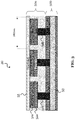
- FIG. 4 shows a cross-section of an optical device 30 according to an embodiment of the invention, which bases on the optical device 30 shown in FIG. 3 . Same elements in FIG. 3 and FIG. 4 share the same reference signs and function likewise.
- FIG. 4 shows the optical device 30 as resulting after step 22 of the method 10 shown in FIG. 2 . Namely, after the formation of the top contact 35 at step 21, further process steps might be implemented at step 22, e.g. adding a damascene metallization grid 40 for better current and heat distribution.
- the metallization grid 40 may be electrically connected to the top contact 35 from above, and can thus serve as a current and heat distributor.
- the grid 40 may comprise a plurality of transparent openings 42, each transparent opening 42 being related to, particularly positioned above, one of the plurality of compound semiconductor LEDs or PDs 31a.
- Each transparent opening 42 may be configured to pass at least the light emitted by the LED 31a it is related to, or the light that the PD 31a it is related to should capture.
- the metallization grid 40 may be connected to determined regions of a top surface of the top contact 35, wherein, the determined regions are positioned above the spaces between adjacent LEDs or PDs 31a in the array 31.
- the grid 40 may have a plurality of vertical posts 41, the vertical posts 41 being positioned above the spaces between the plurality of LEDs or PDs 31a and configured to separate adjacent LEDs or PDs 31a of the array 31 from each other.
- the transparent openings 42 may be provided above the vertical posts 41.
- the vertical posts 41 help to, for instance, avoid that light emitted by one of the LEDs 31a exits the transparent opening 42 related to another one of the LEDs 31a.
- the vertical posts 41 may be light absorbing, at least for the LED light.
- the posts 41 may be coated with an absorptive layer, e.g. carbon layer.
- a distance between the posts 41 arranged above spaces between different adjacent LEDs or PDs 31s may be in the order of the LED/PD pixel pitch, particularly may be 3 ⁇ m as shown.
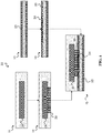
- FIG. 5 shows in (a) an optical device 30 according to the embodiment of the invention in a top view, and shows in (b) a cross-section of an optical device 30 according to an embodiment of the invention.
- the two shown optical devices 30 may be the same and may base on the optical device 30 shown in FIG. 3 .
- FIG. 5 (a) shows a top level layout of the optical device 30 including the first semiconductor part 30a with the array 31 and the top contact 35, and the second semiconductor part 30b with the CMOS IC 33.
- the active array 31 a very dense, high aperture array of compound semiconductor ⁇ LEDs or ⁇ PDs 31a can be generated without any VIAs.
- the top contact 35 of the array 31 needs to be connected to the CMOS IC 33 as well, so that the CMOS IC can drive and/or readout the array 31. This connection, however, is fabricated outside e.g. the emissive LED array 31 area.
- the top contact 35 may be electrically connected to the CMOS IC 33 by at least one electrical connection element 50 arranged outside of the LED/PD array 31.
- the electrical connection element 50 may be a VIA. In the top view of the array 31, the VIA 50 may surround the array 31.
- the CMOS IC 33 is thus configured to drive/readout each LED or PD 31a with the top contact 35 and the bottom contact 32 (32a+32b) connected to that LED or PD 31a.
- the at least one electrical connection element 50 is also illustrated in FIG. 5 (b) .
- here exemplarily four electrical connection elements 50 are shown, two on each side of the array 31 in the cross-sectional view.
- Each electrical connection element 50 connects the top contact 35 to the CMOS IC 33.
- the top contact 35 may electrically be separated into different top contact regions, e.g. each contact region being connected with one electrical connection element 50 to the CMOS IC 33.
- each of the electrical connection elements 50 is passed by the array 31.
- the electrical connection elements 50 may also be passed around the array 31, particularly in a non-straight manner.
- the four electrical connection elements 50 are arranged with a lower density than the plurality of first contacts 32 and second contacts 34, respectively. This means, the electrical connection elements 50 are spaced further apart from another than the first contacts 32 and second contacts 34, respectively.
- a distance between two adjacent VIAs 32b may be in the order of the pixel pitch between 1-10 ⁇ m, but preferably 3 ⁇ m or less.
- a distance between adjacent electrical connection elements 50 may be larger than this 3 ⁇ m, and even larger than 10 ⁇ m. Consequently, fewer electrical connection elements 50 are arranged in a certain area than first and second contacts 32 and 34, respectively.
- FIG. 6 shows an LED device 30, particularly a ⁇ LED device, according to an embodiment of the invention in a cross-section. Same elements in FIG. 6 and the previous figures share the same reference signs and function likewise.
- the LED device 30 of FIG. 6 has also the metallization grid 40 shown in FIG. 4 , but could also be designed without it like the LED device 30 in FIG. 3 .
- the LED device 30 shown in FIG. 6 is obtained by a partial MESA etch as described above with respect to FIG. 2 .
- the epi LED layers include, for each LED 31a of the LED array 31, quantum well layers 61, a first highly-doped contact layer 60 (exemplarily shown to be a n-type contact layer but could also be p-type) below the quantum well layers 61, and a second highly-doped contact layer 62 (exemplarily a p-type contact layer but could also be n-type) above the quantum well layers 61.
- the quantum well layers 61 and the second-highly doped contact layer 62 were not etched in the partial MESA etch, i.e.
- the first highly-doped contact layer 60 was etched during the partial MESA etch, so that each of the LEDs 31a in the LED array 31 has an individual highly-doped contact layer 60.
- the second highly-doped contact layer 62 above the quantum well layers 61 is contacted by the (common) top contact 35 from above.
- Each first highly-doped contact layer 60 is contacted by a bottom contact 32a from below - and further through a VIA 32b, across the bonding surface 63 between the first semiconductor part 30a and the second semiconductor part 30b, and through one of the second contacts 33 to the CMOS IC 33.
- the method 10 and LED device 30 allow achieving an increased resolution (i.e. reduced LED pixel pitch) with very little brightness drop of the scaled LED pixels.
- the method 10 is fully compatible with an advanced 300 mm fab.
- a logic wafer can be used in a more advanced node e.g. 55nm, which enables even more performance.
Landscapes
- Led Devices (AREA)
Priority Applications (3)
| Application Number | Priority Date | Filing Date | Title |
|---|---|---|---|
| EP18211315.9A EP3667721A1 (fr) | 2018-12-10 | 2018-12-10 | Procédé de fabrication d'un dispositif optique |
| US16/708,014 US11316066B2 (en) | 2018-12-10 | 2019-12-09 | Method for fabricating an optical device |
| CN201911261243.XA CN111293133B (zh) | 2018-12-10 | 2019-12-10 | 用于制造光学器件的方法 |
Applications Claiming Priority (1)
| Application Number | Priority Date | Filing Date | Title |
|---|---|---|---|
| EP18211315.9A EP3667721A1 (fr) | 2018-12-10 | 2018-12-10 | Procédé de fabrication d'un dispositif optique |
Publications (1)
| Publication Number | Publication Date |
|---|---|
| EP3667721A1 true EP3667721A1 (fr) | 2020-06-17 |
Family
ID=64664870
Family Applications (1)
| Application Number | Title | Priority Date | Filing Date |
|---|---|---|---|
| EP18211315.9A Pending EP3667721A1 (fr) | 2018-12-10 | 2018-12-10 | Procédé de fabrication d'un dispositif optique |
Country Status (3)
| Country | Link |
|---|---|
| US (1) | US11316066B2 (fr) |
| EP (1) | EP3667721A1 (fr) |
| CN (1) | CN111293133B (fr) |
Cited By (2)
| Publication number | Priority date | Publication date | Assignee | Title |
|---|---|---|---|---|
| EP4303926A1 (fr) | 2022-07-06 | 2024-01-10 | Micledi Microdisplays BV | Procédé de fabrication de dispositifs polychromes et dispositif d'affichage polychrome |
| WO2024008403A1 (fr) | 2022-07-06 | 2024-01-11 | Micledi Microdisplays Bv | Procédé de fabrication de dispositifs polychromes et d'un dispositif d'affichage polychrome |
Families Citing this family (6)
| Publication number | Priority date | Publication date | Assignee | Title |
|---|---|---|---|---|
| EP4186098A4 (fr) * | 2020-07-21 | 2024-10-09 | Lumileds LLC | Procédés de fabrication d'un dispositif électroluminescent avec incrustation métallique et contacts supérieurs |
| CN112582294B (zh) * | 2020-12-09 | 2023-11-17 | 苏州芯聚半导体有限公司 | 微发光二极管晶粒的定位和去除方法及设备 |
| CN118679586B (zh) * | 2022-01-31 | 2026-02-13 | 上海显耀显示科技股份有限公司 | 微型led、微型led阵列面板及其制造方法 |
| KR20240141202A (ko) * | 2022-01-31 | 2024-09-25 | 제이드 버드 디스플레이(상하이) 리미티드 | 마이크로 led, 마이크로 led 어레이 패널 및 그의 제조 방법 |
| WO2025217789A1 (fr) * | 2024-04-16 | 2025-10-23 | Jade Bird Display (shanghai) Limited | Réseau de micro-del et écran d'affichage à micro-del |
| WO2025217788A1 (fr) * | 2024-04-16 | 2025-10-23 | Jade Bird Display (shanghai) Limited | Réseau de micro-del et écran d'affichage à micro-del |
Citations (6)
| Publication number | Priority date | Publication date | Assignee | Title |
|---|---|---|---|---|
| WO2007034367A1 (fr) * | 2005-09-19 | 2007-03-29 | Koninklijke Philips Electronics N.V. | Dispositif photoemetteur de couleur variable |
| WO2010149027A1 (fr) * | 2009-06-22 | 2010-12-29 | Industrial Technology Research Institute | Matrice d'unités électroluminescentes, son procédé de fabrication et appareil de projection |
| TW201122708A (en) * | 2009-12-31 | 2011-07-01 | Ind Tech Res Inst | Light-emitting unit array, mothod for fabricating the same and projection apparatus |
| US20160141469A1 (en) * | 2014-11-18 | 2016-05-19 | Commissariat â l'Energie Atomique et aux Energies Alternatives | Optoelectronic device with light-emitting diodes |
| WO2017068029A1 (fr) * | 2015-10-22 | 2017-04-27 | Commissariat A L'energie Atomique Et Aux Energies Alternatives | Diode micro-electronique a surface active optimisee |
| US20180308832A1 (en) * | 2017-04-25 | 2018-10-25 | Lumens Co., Ltd. | Micro led display device and method of fabricating the same |
Family Cites Families (28)
| Publication number | Priority date | Publication date | Assignee | Title |
|---|---|---|---|---|
| DE602004028115D1 (de) | 2003-05-02 | 2010-08-26 | Univ College Cork Nat Univ Ie | Lichtemittierende mesastrukturen mit hohem höhe-zu-breite-verhältnis und quasi-parabolischen seitenwänden und ihre herstellung |
| US6984816B2 (en) * | 2003-08-13 | 2006-01-10 | Motorola, Inc. | Vertically integrated photosensor for CMOS imagers |
| US8426227B1 (en) | 2011-11-18 | 2013-04-23 | LuxVue Technology Corporation | Method of forming a micro light emitting diode array |
| GB201202222D0 (en) | 2012-02-09 | 2012-03-28 | Mled Ltd | Enhanced light extraction |
| US8629524B2 (en) * | 2012-04-27 | 2014-01-14 | Taiwan Semiconductor Manufacturing Company, Ltd. | Apparatus for vertically integrated backside illuminated image sensors |
| US8957358B2 (en) * | 2012-04-27 | 2015-02-17 | Taiwan Semiconductor Manufacturing Company, Ltd. | CMOS image sensor chips with stacked scheme and methods for forming the same |
| US9406711B2 (en) * | 2012-06-15 | 2016-08-02 | Taiwan Semiconductor Manufacturing Company, Ltd. | Apparatus and method for backside illuminated image sensors |
| JP6112472B2 (ja) * | 2013-01-15 | 2017-04-12 | 住友電気工業株式会社 | 受光デバイスの製造方法 |
| US9035279B2 (en) | 2013-07-08 | 2015-05-19 | LuxVue Technology Corporation | Micro device with stabilization post |
| US10374128B2 (en) * | 2013-12-12 | 2019-08-06 | Terahertz Device Corporation | Electrical contacts to light-emitting diodes for improved current spreading and injection |
| WO2015165048A1 (fr) * | 2014-04-29 | 2015-11-05 | 陈振贤 | Element a reseau de del verticales integrant des structures epitaxiales de del et un substrat de boitier de del |
| US9831387B2 (en) * | 2014-06-14 | 2017-11-28 | Hiphoton Co., Ltd. | Light engine array |
| US9653642B1 (en) * | 2014-12-23 | 2017-05-16 | Soraa Laser Diode, Inc. | Manufacturable RGB display based on thin film gallium and nitrogen containing light emitting diodes |
| US10014340B2 (en) * | 2015-12-28 | 2018-07-03 | Taiwan Semiconductor Manufacturing Co., Ltd. | Stacked SPAD image sensor |
| US9923013B1 (en) * | 2016-11-18 | 2018-03-20 | Taiwan Semiconductor Manufacturing Company Ltd. | Sensor device, image sensor array and manufacturing method of sensor device |
| CN106876406B (zh) * | 2016-12-30 | 2023-08-08 | 上海君万微电子科技有限公司 | 基于iii-v族氮化物半导体的led全彩显示器件结构及制备方法 |
| US10629577B2 (en) * | 2017-03-16 | 2020-04-21 | Invensas Corporation | Direct-bonded LED arrays and applications |
| US10636930B2 (en) * | 2017-09-29 | 2020-04-28 | Taiwan Semiconductor Manufacturing Company Ltd. | SPAD image sensor and associated fabricating method |
| US10373999B2 (en) * | 2017-09-29 | 2019-08-06 | Taiwan Semiconductor Manufacturing Company Ltd. | Image sensor and associated fabricating method |
| US10204950B1 (en) * | 2017-09-29 | 2019-02-12 | Taiwan Semiconductor Manufacturing Company Ltd. | SPAD image sensor and associated fabricating method |
| US10020422B1 (en) | 2017-09-29 | 2018-07-10 | Oculus Vr, Llc | Mesa shaped micro light emitting diode with bottom N-contact |
| US10672820B2 (en) * | 2017-11-23 | 2020-06-02 | Taiwan Semiconductor Manufacturing Co., Ltd. | Hybrid bonded structure |
| WO2019132958A1 (fr) * | 2017-12-29 | 2019-07-04 | Intel Corporation | Ensembles microélectroniques |
| US11404400B2 (en) * | 2018-01-24 | 2022-08-02 | Apple Inc. | Micro LED based display panel |
| US10437402B1 (en) * | 2018-03-27 | 2019-10-08 | Shaoher Pan | Integrated light-emitting pixel arrays based devices by bonding |
| US11605760B2 (en) * | 2018-05-21 | 2023-03-14 | Intel Corporation | Micro light-emitting diode displays having nanophosphors |
| US11342479B2 (en) * | 2018-09-11 | 2022-05-24 | Facebook Technologies, Llc | Reducing bowing of materials before wafer-to-wafer bonding for LED manufacturing |
| JP6915029B2 (ja) * | 2018-11-30 | 2021-08-04 | シャープ株式会社 | マイクロ発光素子及び画像表示素子 |
-
2018
- 2018-12-10 EP EP18211315.9A patent/EP3667721A1/fr active Pending
-
2019
- 2019-12-09 US US16/708,014 patent/US11316066B2/en active Active
- 2019-12-10 CN CN201911261243.XA patent/CN111293133B/zh active Active
Patent Citations (8)
| Publication number | Priority date | Publication date | Assignee | Title |
|---|---|---|---|---|
| WO2007034367A1 (fr) * | 2005-09-19 | 2007-03-29 | Koninklijke Philips Electronics N.V. | Dispositif photoemetteur de couleur variable |
| WO2010149027A1 (fr) * | 2009-06-22 | 2010-12-29 | Industrial Technology Research Institute | Matrice d'unités électroluminescentes, son procédé de fabrication et appareil de projection |
| TW201122708A (en) * | 2009-12-31 | 2011-07-01 | Ind Tech Res Inst | Light-emitting unit array, mothod for fabricating the same and projection apparatus |
| US20160141469A1 (en) * | 2014-11-18 | 2016-05-19 | Commissariat â l'Energie Atomique et aux Energies Alternatives | Optoelectronic device with light-emitting diodes |
| EP3024030A1 (fr) * | 2014-11-18 | 2016-05-25 | Commissariat A L'energie Atomique Et Aux Energies Alternatives | Dispositif optoélectronique à diodes électroluminescentes et son procédé de fabrication |
| WO2017068029A1 (fr) * | 2015-10-22 | 2017-04-27 | Commissariat A L'energie Atomique Et Aux Energies Alternatives | Diode micro-electronique a surface active optimisee |
| US20180315738A1 (en) * | 2015-10-22 | 2018-11-01 | Commissaria A L'energie Atomique Et Aux Energies Alternatives | Microelectronic diode with optimised active surface |
| US20180308832A1 (en) * | 2017-04-25 | 2018-10-25 | Lumens Co., Ltd. | Micro led display device and method of fabricating the same |
Cited By (2)
| Publication number | Priority date | Publication date | Assignee | Title |
|---|---|---|---|---|
| EP4303926A1 (fr) | 2022-07-06 | 2024-01-10 | Micledi Microdisplays BV | Procédé de fabrication de dispositifs polychromes et dispositif d'affichage polychrome |
| WO2024008403A1 (fr) | 2022-07-06 | 2024-01-11 | Micledi Microdisplays Bv | Procédé de fabrication de dispositifs polychromes et d'un dispositif d'affichage polychrome |
Also Published As
| Publication number | Publication date |
|---|---|
| US20200185566A1 (en) | 2020-06-11 |
| CN111293133A (zh) | 2020-06-16 |
| CN111293133B (zh) | 2024-07-30 |
| US11316066B2 (en) | 2022-04-26 |
Similar Documents
| Publication | Publication Date | Title |
|---|---|---|
| US11316066B2 (en) | Method for fabricating an optical device | |
| US11843087B2 (en) | Vertical solid-state transducers and high voltage solid-state transducers having buried contacts and associated systems and methods | |
| US12490564B2 (en) | Vertical solid-state transducers having backside terminals and associated systems and methods | |
| US10734439B2 (en) | Method for producing an optoelectronic device comprising a plurality of gallium nitride diodes | |
| US10037981B2 (en) | Integrated display system with multi-color light emitting diodes (LEDs) | |
| CN113497161B (zh) | 光发射和/或光接收二极管阵列器件 | |
| US20190363520A1 (en) | Vertical Emitters Integrated on Silicon Control Backplane | |
| US8283215B2 (en) | Semiconductor and optoelectronic devices | |
| US20240097087A1 (en) | Method of Transferring Patterned Micro-LED Die onto a Silicon Carrier for Wafer-to-Wafer Hybrid Bonding to a CMOS Backplane | |
| US8598611B2 (en) | Vertical solid-state transducers and solid-state transducer arrays having backside terminals and associated systems and methods | |
| US20120091474A1 (en) | Novel semiconductor and optoelectronic devices | |
| WO2024119056A1 (fr) | Dispositif d'affichage comprenant des pixels de dispositif électroluminescent multicolore à structure latérale et son procédé de fabrication | |
| EP4303926A1 (fr) | Procédé de fabrication de dispositifs polychromes et dispositif d'affichage polychrome | |
| CN119522649A (zh) | 用于制造多色器件和多色显示设备的方法 | |
| CN120897602A (zh) | 显示器件及其制备方法、以及电子装置 |
Legal Events
| Date | Code | Title | Description |
|---|---|---|---|
| PUAI | Public reference made under article 153(3) epc to a published international application that has entered the european phase |
Free format text: ORIGINAL CODE: 0009012 |
|
| STAA | Information on the status of an ep patent application or granted ep patent |
Free format text: STATUS: THE APPLICATION HAS BEEN PUBLISHED |
|
| AK | Designated contracting states |
Kind code of ref document: A1 Designated state(s): AL AT BE BG CH CY CZ DE DK EE ES FI FR GB GR HR HU IE IS IT LI LT LU LV MC MK MT NL NO PL PT RO RS SE SI SK SM TR |
|
| AX | Request for extension of the european patent |
Extension state: BA ME |
|
| STAA | Information on the status of an ep patent application or granted ep patent |
Free format text: STATUS: REQUEST FOR EXAMINATION WAS MADE |
|
| 17P | Request for examination filed |
Effective date: 20201217 |
|
| RBV | Designated contracting states (corrected) |
Designated state(s): AL AT BE BG CH CY CZ DE DK EE ES FI FR GB GR HR HU IE IS IT LI LT LU LV MC MK MT NL NO PL PT RO RS SE SI SK SM TR |
|
| STAA | Information on the status of an ep patent application or granted ep patent |
Free format text: STATUS: EXAMINATION IS IN PROGRESS |
|
| 17Q | First examination report despatched |
Effective date: 20220211 |