EP3667745A1 - Procédé d'obtention de diodes électroluminescentes reconstituées sur un substrat de support - Google Patents
Procédé d'obtention de diodes électroluminescentes reconstituées sur un substrat de support Download PDFInfo
- Publication number
- EP3667745A1 EP3667745A1 EP18211326.6A EP18211326A EP3667745A1 EP 3667745 A1 EP3667745 A1 EP 3667745A1 EP 18211326 A EP18211326 A EP 18211326A EP 3667745 A1 EP3667745 A1 EP 3667745A1
- Authority
- EP
- European Patent Office
- Prior art keywords
- stack
- led
- substrate
- bonding
- carrier substrate
- Prior art date
- Legal status (The legal status is an assumption and is not a legal conclusion. Google has not performed a legal analysis and makes no representation as to the accuracy of the status listed.)
- Granted
Links
Images


Classifications
-
- H—ELECTRICITY
- H10—SEMICONDUCTOR DEVICES; ELECTRIC SOLID-STATE DEVICES NOT OTHERWISE PROVIDED FOR
- H10H—INORGANIC LIGHT-EMITTING SEMICONDUCTOR DEVICES HAVING POTENTIAL BARRIERS
- H10H20/00—Individual inorganic light-emitting semiconductor devices having potential barriers, e.g. light-emitting diodes [LED]
- H10H20/01—Manufacture or treatment
- H10H20/011—Manufacture or treatment of bodies, e.g. forming semiconductor layers
- H10H20/018—Bonding of wafers
-
- H—ELECTRICITY
- H10—SEMICONDUCTOR DEVICES; ELECTRIC SOLID-STATE DEVICES NOT OTHERWISE PROVIDED FOR
- H10H—INORGANIC LIGHT-EMITTING SEMICONDUCTOR DEVICES HAVING POTENTIAL BARRIERS
- H10H20/00—Individual inorganic light-emitting semiconductor devices having potential barriers, e.g. light-emitting diodes [LED]
- H10H20/80—Constructional details
- H10H20/85—Packages
-
- H—ELECTRICITY
- H10—SEMICONDUCTOR DEVICES; ELECTRIC SOLID-STATE DEVICES NOT OTHERWISE PROVIDED FOR
- H10W—GENERIC PACKAGES, INTERCONNECTIONS, CONNECTORS OR OTHER CONSTRUCTIONAL DETAILS OF DEVICES COVERED BY CLASS H10
- H10W99/00—Subject matter not provided for in other groups of this subclass
-
- H—ELECTRICITY
- H10—SEMICONDUCTOR DEVICES; ELECTRIC SOLID-STATE DEVICES NOT OTHERWISE PROVIDED FOR
- H10H—INORGANIC LIGHT-EMITTING SEMICONDUCTOR DEVICES HAVING POTENTIAL BARRIERS
- H10H20/00—Individual inorganic light-emitting semiconductor devices having potential barriers, e.g. light-emitting diodes [LED]
- H10H20/01—Manufacture or treatment
-
- H—ELECTRICITY
- H10—SEMICONDUCTOR DEVICES; ELECTRIC SOLID-STATE DEVICES NOT OTHERWISE PROVIDED FOR
- H10H—INORGANIC LIGHT-EMITTING SEMICONDUCTOR DEVICES HAVING POTENTIAL BARRIERS
- H10H20/00—Individual inorganic light-emitting semiconductor devices having potential barriers, e.g. light-emitting diodes [LED]
- H10H20/80—Constructional details
- H10H20/81—Bodies
- H10H20/822—Materials of the light-emitting regions
- H10H20/824—Materials of the light-emitting regions comprising only Group III-V materials, e.g. GaP
- H10H20/825—Materials of the light-emitting regions comprising only Group III-V materials, e.g. GaP containing nitrogen, e.g. GaN
-
- H—ELECTRICITY
- H10—SEMICONDUCTOR DEVICES; ELECTRIC SOLID-STATE DEVICES NOT OTHERWISE PROVIDED FOR
- H10H—INORGANIC LIGHT-EMITTING SEMICONDUCTOR DEVICES HAVING POTENTIAL BARRIERS
- H10H29/00—Integrated devices, or assemblies of multiple devices, comprising at least one light-emitting semiconductor element covered by group H10H20/00
- H10H29/10—Integrated devices comprising at least one light-emitting semiconductor component covered by group H10H20/00
- H10H29/14—Integrated devices comprising at least one light-emitting semiconductor component covered by group H10H20/00 comprising multiple light-emitting semiconductor components
-
- H—ELECTRICITY
- H10—SEMICONDUCTOR DEVICES; ELECTRIC SOLID-STATE DEVICES NOT OTHERWISE PROVIDED FOR
- H10H—INORGANIC LIGHT-EMITTING SEMICONDUCTOR DEVICES HAVING POTENTIAL BARRIERS
- H10H29/00—Integrated devices, or assemblies of multiple devices, comprising at least one light-emitting semiconductor element covered by group H10H20/00
- H10H29/10—Integrated devices comprising at least one light-emitting semiconductor component covered by group H10H20/00
- H10H29/14—Integrated devices comprising at least one light-emitting semiconductor component covered by group H10H20/00 comprising multiple light-emitting semiconductor components
- H10H29/142—Two-dimensional arrangements, e.g. asymmetric LED layout
-
- H—ELECTRICITY
- H10—SEMICONDUCTOR DEVICES; ELECTRIC SOLID-STATE DEVICES NOT OTHERWISE PROVIDED FOR
- H10W—GENERIC PACKAGES, INTERCONNECTIONS, CONNECTORS OR OTHER CONSTRUCTIONAL DETAILS OF DEVICES COVERED BY CLASS H10
- H10W90/00—Package configurations
-
- H—ELECTRICITY
- H10—SEMICONDUCTOR DEVICES; ELECTRIC SOLID-STATE DEVICES NOT OTHERWISE PROVIDED FOR
- H10H—INORGANIC LIGHT-EMITTING SEMICONDUCTOR DEVICES HAVING POTENTIAL BARRIERS
- H10H20/00—Individual inorganic light-emitting semiconductor devices having potential barriers, e.g. light-emitting diodes [LED]
- H10H20/01—Manufacture or treatment
- H10H20/036—Manufacture or treatment of packages
-
- H—ELECTRICITY
- H10—SEMICONDUCTOR DEVICES; ELECTRIC SOLID-STATE DEVICES NOT OTHERWISE PROVIDED FOR
- H10W—GENERIC PACKAGES, INTERCONNECTIONS, CONNECTORS OR OTHER CONSTRUCTIONAL DETAILS OF DEVICES COVERED BY CLASS H10
- H10W72/00—Interconnections or connectors in packages
- H10W72/01—Manufacture or treatment
- H10W72/019—Manufacture or treatment of bond pads
-
- H—ELECTRICITY
- H10—SEMICONDUCTOR DEVICES; ELECTRIC SOLID-STATE DEVICES NOT OTHERWISE PROVIDED FOR
- H10W—GENERIC PACKAGES, INTERCONNECTIONS, CONNECTORS OR OTHER CONSTRUCTIONAL DETAILS OF DEVICES COVERED BY CLASS H10
- H10W72/00—Interconnections or connectors in packages
- H10W72/01—Manufacture or treatment
- H10W72/019—Manufacture or treatment of bond pads
- H10W72/01951—Changing the shapes of bond pads
-
- H—ELECTRICITY
- H10—SEMICONDUCTOR DEVICES; ELECTRIC SOLID-STATE DEVICES NOT OTHERWISE PROVIDED FOR
- H10W—GENERIC PACKAGES, INTERCONNECTIONS, CONNECTORS OR OTHER CONSTRUCTIONAL DETAILS OF DEVICES COVERED BY CLASS H10
- H10W72/00—Interconnections or connectors in packages
- H10W72/01—Manufacture or treatment
- H10W72/0198—Manufacture or treatment batch processes
-
- H—ELECTRICITY
- H10—SEMICONDUCTOR DEVICES; ELECTRIC SOLID-STATE DEVICES NOT OTHERWISE PROVIDED FOR
- H10W—GENERIC PACKAGES, INTERCONNECTIONS, CONNECTORS OR OTHER CONSTRUCTIONAL DETAILS OF DEVICES COVERED BY CLASS H10
- H10W72/00—Interconnections or connectors in packages
- H10W72/90—Bond pads, in general
-
- H—ELECTRICITY
- H10—SEMICONDUCTOR DEVICES; ELECTRIC SOLID-STATE DEVICES NOT OTHERWISE PROVIDED FOR
- H10W—GENERIC PACKAGES, INTERCONNECTIONS, CONNECTORS OR OTHER CONSTRUCTIONAL DETAILS OF DEVICES COVERED BY CLASS H10
- H10W72/00—Interconnections or connectors in packages
- H10W72/90—Bond pads, in general
- H10W72/951—Materials of bond pads
- H10W72/953—Materials of bond pads not comprising solid metals or solid metalloids, e.g. polymers, ceramics or liquids
-
- H—ELECTRICITY
- H10—SEMICONDUCTOR DEVICES; ELECTRIC SOLID-STATE DEVICES NOT OTHERWISE PROVIDED FOR
- H10W—GENERIC PACKAGES, INTERCONNECTIONS, CONNECTORS OR OTHER CONSTRUCTIONAL DETAILS OF DEVICES COVERED BY CLASS H10
- H10W80/00—Direct bonding of chips, wafers or substrates
- H10W80/011—Manufacture or treatment of pads or other interconnections to be direct bonded
- H10W80/041—Thermally treating
-
- H—ELECTRICITY
- H10—SEMICONDUCTOR DEVICES; ELECTRIC SOLID-STATE DEVICES NOT OTHERWISE PROVIDED FOR
- H10W—GENERIC PACKAGES, INTERCONNECTIONS, CONNECTORS OR OTHER CONSTRUCTIONAL DETAILS OF DEVICES COVERED BY CLASS H10
- H10W80/00—Direct bonding of chips, wafers or substrates
- H10W80/102—Controlling the environment during the bonding, e.g. the temperature or pressure
-
- H—ELECTRICITY
- H10—SEMICONDUCTOR DEVICES; ELECTRIC SOLID-STATE DEVICES NOT OTHERWISE PROVIDED FOR
- H10W—GENERIC PACKAGES, INTERCONNECTIONS, CONNECTORS OR OTHER CONSTRUCTIONAL DETAILS OF DEVICES COVERED BY CLASS H10
- H10W80/00—Direct bonding of chips, wafers or substrates
- H10W80/301—Bonding techniques, e.g. hybrid bonding
- H10W80/327—Bonding techniques, e.g. hybrid bonding characterised by the direct bonding of insulating parts, e.g. of silicon oxide layers
-
- H—ELECTRICITY
- H10—SEMICONDUCTOR DEVICES; ELECTRIC SOLID-STATE DEVICES NOT OTHERWISE PROVIDED FOR
- H10W—GENERIC PACKAGES, INTERCONNECTIONS, CONNECTORS OR OTHER CONSTRUCTIONAL DETAILS OF DEVICES COVERED BY CLASS H10
- H10W80/00—Direct bonding of chips, wafers or substrates
- H10W80/301—Bonding techniques, e.g. hybrid bonding
- H10W80/331—Bonding techniques, e.g. hybrid bonding characterised by the application of energy for connecting
- H10W80/333—Compression bonding
-
- H—ELECTRICITY
- H10—SEMICONDUCTOR DEVICES; ELECTRIC SOLID-STATE DEVICES NOT OTHERWISE PROVIDED FOR
- H10W—GENERIC PACKAGES, INTERCONNECTIONS, CONNECTORS OR OTHER CONSTRUCTIONAL DETAILS OF DEVICES COVERED BY CLASS H10
- H10W80/00—Direct bonding of chips, wafers or substrates
- H10W80/301—Bonding techniques, e.g. hybrid bonding
- H10W80/331—Bonding techniques, e.g. hybrid bonding characterised by the application of energy for connecting
- H10W80/333—Compression bonding
- H10W80/334—Thermocompression bonding
Definitions
- the present invention presents relates to the technical field of Light Emitting Diode (LED) devices, in particular of micro-LED ( ⁇ LED) devices.
- the invention proposes a method for obtaining one or more LED devices reconstituted over a carrier substrate.
- a carrier substrate For example, one or more GaN LED devices reconstituted over a 300 mm silicon-based carrier wafer.
- the proposed method includes particularly a bonding of one or more compound semiconductors stacks to the carrier substrate, wherein the LED devices may then be completed from the bonded compound semiconductor stacks.
- the method is particularly applicable in a process for fabricating a ⁇ LED device suitable for a ⁇ LED display.
- a material stack or material layers, particularly semiconductor material may be first bond to a carrier substrate.
- the obtained material stacks reconstituted over the carrier substrate may then be processed more efficiently or easier to complete the device.
- a conventional method for such bonding of material stacks or layers to a carrier substrate is, for example, described in US 2017/0301646 A1 .
- the bonding method includes a pre-bond annealing step at a temperature between 400-450°C and a post-bond annealing step at a temperature of 250°C or less.
- the method is described for creating a silicon-to-silicon bond, and is especially suitable for bonding two silicon wafers comprising Front End of Line (FEOL) and/or Back End of Line (BEOL) layers.
- compound semiconductor stacks e.g. made from III-V or II-VI semiconductor material
- a silicon-based carrier substrate there is a material mismatch of the bonded parts. This may cause problems, if the further processing of the bonded stacks into the LED devices requires a high-temperature processing step.
- a p-type contact formation onto GaN-based stacks bonded to the wafer is usually required.
- the temperature applied during this contact formation process is typically as high as 550°C.
- the bonds created between the compound semiconductor stacks and the silicon-based carrier substrate may deteriorate during the high-temperature processing step.
- the different thermal expansion coefficients lead to a large thermal stress, which may weaken or even destroy the bonds between the stacks and the carrier substrate.
- embodiments of the present invention aim to improve the conventional process of fabricating a LED device, particularly of obtaining one or more LED devices reconstituted over a silicon-based carrier substrate.
- An objective is in particular to provide a bonding method that creates a bond between one or more compound semiconductor stacks and a silicon-based carrier substrate, which is strong enough to withstand a subsequent high-temperature processing step, which may be used to manufacture an LED device per each stack.
- the embodiments of the invention base on the assumption that the higher the subsequent processing temperature and the associated thermal stress is, the higher the bond strength of the bond between the carrier substrate and the one or more compound semiconductor stacks has to be, in order to counter the thermal stress. Further, the embodiments of the invention base on the recognition of the specific application scenario of fabricating LED devices, wherein a compound semiconductor stack, from which an LED device is made, includes no FEOL and/or BEOL structuring. Further, wherein the silicon-based carrier substrate may be a blank, unstructured substrate.
- the solution provided by the embodiments of the invention is generally to use a bonding material with a maximum bond strength, particularly SiCN, and to perform - after the bonding of stacks and carrier substrate - a post-bond annealing at a temperature, which is in the range of a maximum temperature of subsequently required processing, e.g. is at least as high as the temperature required for the above-mentioned contact formation.
- a bonding material with a maximum bond strength particularly SiCN
- a first aspect of the invention relates to a method for obtaining one or more LED devices reconstituted over a carrier substrate, the method comprising: providing a silicon-based semiconductor substrate as the carrier substrate, providing, per each of the one or more LED devices, a compound semiconductor stack including an LED layer, applying a silicon carbon nitride, SiCN, layer to the stack and the substrate, respectively, bonding the stack to the substrate, wherein the SiCN layer applied to the stack and the SiCN layer applied to the substrate are contacted, annealing, after bonding, the bonded stack and substrate at a temperature equal to or higher than a processing temperature for completing the LED device from the stack, wherein said temperatures are at least 400°C.
- An LED device may include one or more LED, but may also include one or more LED arrays. Thereby, a LED array may be a ⁇ LED array.
- the bonding material SiCN
- a high post-bond annealing temperature of at least 400°C
- a very high bonding strength between the compound semiconductor stack and the silicon-based carrier substrate is achieved.
- the bond will not likely deteriorate during the subsequent completion of the LED device from the stack, which is carried out at high temperatures - but not higher than the post-bond annealing.
- one or more LED devices reconstituted over the carrier substrate can be more reliably obtained, and the process for fabricating LED devices, particularly including a ⁇ LED array each, results in significantly higher yields.
- the high temperature post-bond annealing step which is applied in the method of the first aspect, is well possible because the silicon-based carrier substrate, on which the compound semiconductor stacks are bonded may - in the particular process of fabricating an LED device - only be a temporary carrier without any active structures (e.g. transistors, BEOL). Further, because the used compound semiconductor stacks, which include the LED layers, may still be blank dies without any structuring before they are processed into the LED devices. Any such structures or structuring would severely limit the temperature available for the post-bond annealing, since they would be destroyed or at least harmed.
- active structures e.g. transistors, BEOL
- the bonding method of the first aspect would not be possible in the application scenario of US 2017/0301646 A1 , since there already structured components are bonded together, for which higher post-bond annealing temperatures than the selected 250°C would result in severe degradation of these devices and/or Cu diffusion.
- the annealing, after bonding, is performed at a temperature equal to or higher than 550°C.
- the post-bond annealing temperature is equal to or higher even than the temperature required for fabricating contacts on the compound semiconductor stacks.
- the annealing, after bonding, is performed for a duration of between 30 minutes and 5 hours.
- the annealing may be done for 2 hours at a temperature between 400-550°C.
- the processing temperature for completing the LED device from the stack is equal to or lower than 550°C.
- completing the LED device from the stack comprises forming a top contact on the stack, particularly a p-contact, to contact the LED layer.
- the method may also comprise forming a bottom contact, particularly an n-contact, which may also be done at a temperature as high as 400°C. However, only the top contact can be annealed at a temperature of or above 400C.
- the silicon-based semiconductor substrate is in the form of a 300 mm wafer.
- the silicon-based 300 mm wafer is an unstructured carrier wafer, which does not yet include any FEOL/BEOL layers.
- the carrier wafer allows to obtain a very high number of reconstituted LED devices.
- the compound semiconductor stack comprises a III-V semiconductor material compound, a II-VI semiconductor material compound, or a metal-nitride compound.
- the compound semiconductor stack includes a GaN-based LED layer.
- applying the SiCN layers comprises: forming a SiN layer or a polished dielectric on the stack and the substrate, respectively, and forming the SiCN layers on the respective SiN layers or polished dielectrics.
- the bonding strength of the bond between the one or more compound semiconductor stacks and the silicon-based carrier substrate is further improved.
- the method further comprises performing a planarization of the SiCN layers, before bonding, to obtain a surface roughness of the SiCN layers of below 1 nm.
- the bonding strength of the bond between the one or more compound semiconductor stacks and the silicon-based carrier substrate is further improved, since the formation of chemical bonds is facilitated.
- the method further comprises annealing, before bonding but after applying the SiCN layers, the stack and substrate at a temperature of at least 400°C, particularly between 400-600°C.
- the annealing, before bonding is performed for a duration of between 30 minutes and 5 hours, in particular for a duration of 2 hours.
- the method is a method for obtaining a plurality of LED devices reconstituted over the carrier substrate, wherein a plurality of the compound semiconductor stacks is provided corresponding to each of the plurality of LED devices, bonded to the substrate, and collectively annealed at the temperature equal to or higher than the processing temperature.
- the method is particularly suited to fabricate multiple LED devices, each e.g. including a LED or ⁇ LED array, at the same time.
- the LED device includes a LED array that has an LED pixel pitch equal to or below 3 ⁇ m.
- a LED array in which the LEDs are spaced very closely together, may be processed from each stack.
- ⁇ LED arrays may be used for ⁇ LED displays.
- a thermal budget of annealing after bonding is preferably equal to or higher than a thermal budget of completing the LED device from the stack, and/or a thermal budget of annealing before bonding is preferably equal to or higher than a thermal budget of annealing after bonding.
- a second aspect of the invention relates to a semiconductor structure including one or more LED devices reconstituted over a carrier substrate, wherein the semiconductor structure is obtained by the method of the first aspect or any of its implementations.
- the semiconductor structure of the second aspect which is obtained with the method of the first aspect, can be further processed to obtain one or more LED devices including each a LED array, particularly a ⁇ LED array.
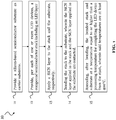
- FIG. 1 shows a method 10 according to an embodiment of the invention in a schematic flow-diagram.
- the method 10 is in particular suitable to obtain one or more LED devices reconstituted over a carrier substrate.
- the LED devices may e.g. include a LED array each, particularly a ⁇ LED array.
- the method 10 can be applied in a fabrication process of such LED devices.
- a silicon-based semiconductor substrate is provided as the carrier substrate.
- the silicon-based carrier substrate may be a pure silicon substrate or a silicon wafer, but may also include or be based on SiN, or may include or be based on SiO 2 .
- the silicon-based carrier substrate may be a complete wafer, particularly a complete 200 mm or 300 mm (Si) wafer.
- the silicon-based substrate is particularly an unstructured wafer.
- one compound semiconductor stack including an LED layer is provided per each LED device (of the one or more LED devices) that is to be reconstituted over the carrier substrate.
- a compound semiconductor stack is provided per LED device to be fabricated. If multiple LED devices are to be formed in parallel, a plurality of semiconductor stacks may be provided in, and before bonding them to the carrier substrate, they should be aligned with respect to the carrier substrate.
- a SiCN layer is applied to the at least one compound semiconductor stack and to the silicon-based carrier substrate, respectively.
- a different SiCN layer is provided to each stack and another SiCN layer is provided to the carrier substrate.
- the at least one compound semiconductor stack is finally bonded to the silicon-based carrier substrate.
- This requires at least contacting the SiCN layers applied on the at least one stack and the carrier substrate, respectively.
- these layers may be forced together by a bonding tool at determined process conditions.
- a post-bond annealing is applied.
- the bonded at least one compound semiconductor stack and the silicon-based carrier substrate are annealed together at a temperature equal to or higher than a processing temperature, which is afterwards used for completing an LED device from a stack.
- the post-bond annealing temperature may be selected to be equal to or higher than a temperature used for contact formation on each of the stacks used to complete the LED devices.
- the post-bond annealing temperature is at least 400°C.
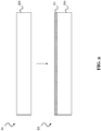
- FIG. 2 shows the first step 11 and a part of the third step 13 of the method 10 shown in FIG. 1 .
- FIG. 2 shows that a silicon-based carrier substrate 20 is provided, and then a SiCN layer 21 is applied to the carrier substrate 20.
- a surface of the silicon-based carrier substrate 20 is at least partly, i.e. at least where the stacks are later to be bonded, covered with the SiCN layer 21, in order to create one or more bonding surfaces.
- a SiN layer or a polished dielectric can be provided, as an intermediate layer, between the substrate surface and the SiCN layer(s) 21.
- FIG. 3 shows the second step 12 and part of the third step 13 of the method 10 shown in FIG. 1 .
- FIG. 3 shows that one or more (here exemplarily two) compound semiconductor stacks 30 are provided, each stack 30 including an LED layer 31.
- the stacks 30 are then applied with a SiCN layer 32 each.
- the SiCN layers 32 can be applied as surface layers to each of the stacks 30.
- a SiN layer or a polished dielectric can be provided in between each stack 30 and the SiCN layer 32, i.e. the SICN 32 layer may be applied onto the SiN layer.
- the SiCN layers 32 define a bonding surface per stack 30.
- the SiCN layers 32 and 21, respectively may be planarized.
- they can be treated with a Chemical Mechanical Planarization (CMP) step, particularly in order to obtain a surface roughness of the SiCN layers 32 and 21 of below 1 nm, or even below 0.5 nm.
- CMP Chemical Mechanical Planarization
- a pre-bond annealing temperature may thereby be at least 400°C, or at least 500°C, or even at least 600°C, in order to achieve an efficient outgassing of the SiCN layers 32 and 21.
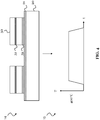
- FIG. 4 shows the fourth step 14 and the fifth step 15 of the method 10 shown in FIG. 1 .
- FIG. 4 shows how the compound semiconductor stacks 30 are aligned with and the bonded to the silicon-based carrier substrate 20.
- the SiCN layers 32 applied to the semiconductor stacks 30 are contacted to the SiCN layer 21 provided on the silicon carrier substrate 20.
- a bond is formed under appropriate process conditions.
- the process conditions may be chosen as for conventionally known bonding techniques, i.e. regarding temperature, ambient pressure and mechanical pressure applied e.g. by a bonding tool, in order to push stacks 30 and carrier substrate 20 together.
- the temperature during bonding may be room temperature or any temperature up to the post-bond annealing temperature and preferably not higher than 500°C.
- Ambient pressure may be low, but preferably not lower as e.g. 10E-6 or 10E-7 mBar.
- the mechanical pressure may be 50-100 KN, but may also be less if sufficient.
- the bonding strength of the created bonds can be significantly increased by then performing an annealing step at a temperature of at least 400°C as schematically shown in FIG. 4 .
- the bonding strength can be further improved by providing the low surface roughness achieved e.g. with CMP, which facilitates the formation of chemical bonds between the bonding surfaces.
- a plurality of compound semiconductor stacks 30 reconstituted over the silicon-based semiconductor carrier substrate 20 is obtained.
- Each of these stacks 30 can then be completed into an LED device, wherein particularly a contact layer 51 may be applied to the free top-surface of each stack 30.
- a p-type contact may be formed on the compound semiconductor stacks 30 bonded to the silicon-based carrier substrate 20.
- completion of the LED device may also include structuring an LED array from each stack 30, i.e. form the LED layer of each stack 30.
- a plurality of LED devices may be reconstituted in a determined alignment or pattern over the carrier substrate 20. For instance, in order to maximize the number of LED device that can be processed in parallel
- Each LED device may finally include a LED array. That is, a LED array may be structured at some point from each stack 30, particularly before forming a top contact on the stack 30, which may then contact the LED array from above.
- the LEDs in such a LED array may be arranged with a LED pixel pitch of between 1-10 ⁇ m, in particular even with a LED pixel pitch that is equal to or below 3 ⁇ m, thus forming a ⁇ LED array.
- Individual LED devices including such a ⁇ LED array each may be obtained, e.g. by dicing and packaging, from the semiconductor structure 50 shown in FIG. 5 .
- the LED devices are useful for a ⁇ LED display as, for instance, used in augmented reality applications.
- the LEDs in the LED array of an LED device may be GaN-based LEDs, or other III-V semiconductor based, or II-VI semiconductor based, or metal-nitride based LEDs.
- the method presented by the invention includes a bonding of a compound semiconductor stack to a silicon-based carrier substrate with an increased bond strength, which can withstand high temperatures used in further processing steps.
- the method is particularly useful in a process for fabricating an LED device with a ⁇ LED array.
Landscapes
- Led Devices (AREA)
Priority Applications (3)
| Application Number | Priority Date | Filing Date | Title |
|---|---|---|---|
| EP18211326.6A EP3667745B1 (fr) | 2018-12-10 | 2018-12-10 | Procédé d'obtention de diodes électroluminescentes reconstituées sur un substrat de support |
| US16/705,702 US11069648B2 (en) | 2018-12-10 | 2019-12-06 | Semiconductor structure and method for obtaining light emitting diodes reconstituted over a carrier substrate |
| CN201911250976.3A CN111293204B (zh) | 2018-12-10 | 2019-12-09 | 用于获得在载体基板上重构的发光二极管的方法 |
Applications Claiming Priority (1)
| Application Number | Priority Date | Filing Date | Title |
|---|---|---|---|
| EP18211326.6A EP3667745B1 (fr) | 2018-12-10 | 2018-12-10 | Procédé d'obtention de diodes électroluminescentes reconstituées sur un substrat de support |
Publications (2)
| Publication Number | Publication Date |
|---|---|
| EP3667745A1 true EP3667745A1 (fr) | 2020-06-17 |
| EP3667745B1 EP3667745B1 (fr) | 2023-03-22 |
Family
ID=64664152
Family Applications (1)
| Application Number | Title | Priority Date | Filing Date |
|---|---|---|---|
| EP18211326.6A Active EP3667745B1 (fr) | 2018-12-10 | 2018-12-10 | Procédé d'obtention de diodes électroluminescentes reconstituées sur un substrat de support |
Country Status (3)
| Country | Link |
|---|---|
| US (1) | US11069648B2 (fr) |
| EP (1) | EP3667745B1 (fr) |
| CN (1) | CN111293204B (fr) |
Cited By (3)
| Publication number | Priority date | Publication date | Assignee | Title |
|---|---|---|---|---|
| EP4016594A1 (fr) | 2020-12-15 | 2022-06-22 | Micledi Microdisplays BV | Procédé et système de production de puces pour une reconstitution de tranche |
| EP4250363A1 (fr) | 2022-03-24 | 2023-09-27 | Micledi Microdisplays BV | Procédé de fabrication de structures mesa et dispositif optique l'utilisant |
| WO2023180230A1 (fr) | 2022-03-24 | 2023-09-28 | Micledi Microdisplays Bv | Procédé de fabrication de structures mesa et dispositif optique l'utilisant |
Families Citing this family (2)
| Publication number | Priority date | Publication date | Assignee | Title |
|---|---|---|---|---|
| GB2593193B (en) * | 2020-03-18 | 2022-03-23 | Plessey Semiconductors Ltd | Light Emitting Diode Structure and High Resolution Monolithic RGB Arrays |
| GB2595250B (en) * | 2020-05-19 | 2022-09-28 | Plessey Semiconductors Ltd | Array of light emitting devices with reduced optical crosstalk |
Citations (3)
| Publication number | Priority date | Publication date | Assignee | Title |
|---|---|---|---|---|
| US20170154881A1 (en) * | 2015-11-30 | 2017-06-01 | Taiwan Semiconductor Manufacturing Company Ltd. | Semiconductor device and method of manufacturing the same |
| US20170301646A1 (en) * | 2014-11-24 | 2017-10-19 | Imec Vzw | Method of bonding semiconductor substrates |
| WO2018169968A1 (fr) * | 2017-03-16 | 2018-09-20 | Invensas Corporation | Réseaux de del à liaison directe et applications |
Family Cites Families (6)
| Publication number | Priority date | Publication date | Assignee | Title |
|---|---|---|---|---|
| US7939422B2 (en) * | 2006-12-07 | 2011-05-10 | Applied Materials, Inc. | Methods of thin film process |
| US8786053B2 (en) * | 2011-01-24 | 2014-07-22 | Soraa, Inc. | Gallium-nitride-on-handle substrate materials and devices and method of manufacture |
| CN104638175A (zh) * | 2013-11-12 | 2015-05-20 | 海洋王照明科技股份有限公司 | 有机电致发光器件及其制备方法 |
| WO2015095614A1 (fr) * | 2013-12-18 | 2015-06-25 | Leupold & Stevens, Inc. | Affichage de réticule à del micro-pixélisé |
| US10685935B2 (en) * | 2017-11-15 | 2020-06-16 | Taiwan Semiconductor Manufacturing Company, Ltd. | Forming metal bonds with recesses |
| KR20190137458A (ko) * | 2018-06-01 | 2019-12-11 | 삼성전자주식회사 | Led를 이용한 디스플레이 모듈 제조방법 |
-
2018
- 2018-12-10 EP EP18211326.6A patent/EP3667745B1/fr active Active
-
2019
- 2019-12-06 US US16/705,702 patent/US11069648B2/en active Active
- 2019-12-09 CN CN201911250976.3A patent/CN111293204B/zh active Active
Patent Citations (3)
| Publication number | Priority date | Publication date | Assignee | Title |
|---|---|---|---|---|
| US20170301646A1 (en) * | 2014-11-24 | 2017-10-19 | Imec Vzw | Method of bonding semiconductor substrates |
| US20170154881A1 (en) * | 2015-11-30 | 2017-06-01 | Taiwan Semiconductor Manufacturing Company Ltd. | Semiconductor device and method of manufacturing the same |
| WO2018169968A1 (fr) * | 2017-03-16 | 2018-09-20 | Invensas Corporation | Réseaux de del à liaison directe et applications |
Cited By (3)
| Publication number | Priority date | Publication date | Assignee | Title |
|---|---|---|---|---|
| EP4016594A1 (fr) | 2020-12-15 | 2022-06-22 | Micledi Microdisplays BV | Procédé et système de production de puces pour une reconstitution de tranche |
| EP4250363A1 (fr) | 2022-03-24 | 2023-09-27 | Micledi Microdisplays BV | Procédé de fabrication de structures mesa et dispositif optique l'utilisant |
| WO2023180230A1 (fr) | 2022-03-24 | 2023-09-28 | Micledi Microdisplays Bv | Procédé de fabrication de structures mesa et dispositif optique l'utilisant |
Also Published As
| Publication number | Publication date |
|---|---|
| EP3667745B1 (fr) | 2023-03-22 |
| US11069648B2 (en) | 2021-07-20 |
| US20200185351A1 (en) | 2020-06-11 |
| CN111293204A (zh) | 2020-06-16 |
| CN111293204B (zh) | 2024-09-17 |
Similar Documents
| Publication | Publication Date | Title |
|---|---|---|
| US11069648B2 (en) | Semiconductor structure and method for obtaining light emitting diodes reconstituted over a carrier substrate | |
| US12199082B2 (en) | Method of direct-bonded optoelectronic devices | |
| US9478707B2 (en) | Method of manufacturing structures of LEDs or solar cells | |
| EP2600389B1 (fr) | Procédé pour la liaison de substrats semi-conducteurs | |
| CN108475626B (zh) | 工程化衬底上的芯片级封装固态器件的剥离工艺 | |
| US20240097087A1 (en) | Method of Transferring Patterned Micro-LED Die onto a Silicon Carrier for Wafer-to-Wafer Hybrid Bonding to a CMOS Backplane | |
| JP7561887B2 (ja) | 発光アレイ | |
| CN110494983B (zh) | 直接键合的led阵列和应用 | |
| US20180366618A1 (en) | Optoelectronic Semiconductor Devices with Enhanced Light Output | |
| US20220336405A1 (en) | Method of Fine Pitch Hybrid Bonding with Dissimilar CTE Wafers and Resulting Structures | |
| TW202504058A (zh) | 用於鍵結兩層體以降低應力之方法 | |
| US20200194612A1 (en) | Method of manufacturing an optoelectronic semiconductor chip and optoelectronic semiconductor chip | |
| US20250301825A1 (en) | Method of manufacturing optoelectronic devices | |
| KR20160034861A (ko) | 반도체 발광소자용 지지 기판 및 이를 이용하는 반도체 발광소자를 제조하는 방법 | |
| KR20150073506A (ko) | 반도체 발광소자용 지지 기판 및 이를 이용하는 반도체 발광소자를 제조하는 방법 |
Legal Events
| Date | Code | Title | Description |
|---|---|---|---|
| PUAI | Public reference made under article 153(3) epc to a published international application that has entered the european phase |
Free format text: ORIGINAL CODE: 0009012 |
|
| STAA | Information on the status of an ep patent application or granted ep patent |
Free format text: STATUS: THE APPLICATION HAS BEEN PUBLISHED |
|
| AK | Designated contracting states |
Kind code of ref document: A1 Designated state(s): AL AT BE BG CH CY CZ DE DK EE ES FI FR GB GR HR HU IE IS IT LI LT LU LV MC MK MT NL NO PL PT RO RS SE SI SK SM TR |
|
| AX | Request for extension of the european patent |
Extension state: BA ME |
|
| STAA | Information on the status of an ep patent application or granted ep patent |
Free format text: STATUS: REQUEST FOR EXAMINATION WAS MADE |
|
| 17P | Request for examination filed |
Effective date: 20201217 |
|
| RBV | Designated contracting states (corrected) |
Designated state(s): AL AT BE BG CH CY CZ DE DK EE ES FI FR GB GR HR HU IE IS IT LI LT LU LV MC MK MT NL NO PL PT RO RS SE SI SK SM TR |
|
| GRAP | Despatch of communication of intention to grant a patent |
Free format text: ORIGINAL CODE: EPIDOSNIGR1 |
|
| STAA | Information on the status of an ep patent application or granted ep patent |
Free format text: STATUS: GRANT OF PATENT IS INTENDED |
|
| RIC1 | Information provided on ipc code assigned before grant |
Ipc: H01L 25/075 20060101ALN20220204BHEP Ipc: H01L 23/00 20060101ALI20220204BHEP Ipc: H01L 33/00 20100101AFI20220204BHEP |
|
| INTG | Intention to grant announced |
Effective date: 20220309 |
|
| GRAJ | Information related to disapproval of communication of intention to grant by the applicant or resumption of examination proceedings by the epo deleted |
Free format text: ORIGINAL CODE: EPIDOSDIGR1 |
|
| STAA | Information on the status of an ep patent application or granted ep patent |
Free format text: STATUS: REQUEST FOR EXAMINATION WAS MADE |
|
| INTC | Intention to grant announced (deleted) | ||
| RIC1 | Information provided on ipc code assigned before grant |
Ipc: H01L 25/075 20060101ALN20220810BHEP Ipc: H01L 23/00 20060101ALI20220810BHEP Ipc: H01L 33/00 20100101AFI20220810BHEP |
|
| GRAP | Despatch of communication of intention to grant a patent |
Free format text: ORIGINAL CODE: EPIDOSNIGR1 |
|
| STAA | Information on the status of an ep patent application or granted ep patent |
Free format text: STATUS: GRANT OF PATENT IS INTENDED |
|
| INTG | Intention to grant announced |
Effective date: 20221004 |
|
| GRAS | Grant fee paid |
Free format text: ORIGINAL CODE: EPIDOSNIGR3 |
|
| GRAA | (expected) grant |
Free format text: ORIGINAL CODE: 0009210 |
|
| STAA | Information on the status of an ep patent application or granted ep patent |
Free format text: STATUS: THE PATENT HAS BEEN GRANTED |
|
| AK | Designated contracting states |
Kind code of ref document: B1 Designated state(s): AL AT BE BG CH CY CZ DE DK EE ES FI FR GB GR HR HU IE IS IT LI LT LU LV MC MK MT NL NO PL PT RO RS SE SI SK SM TR |
|
| REG | Reference to a national code |
Ref country code: GB Ref legal event code: FG4D |
|
| REG | Reference to a national code |
Ref country code: CH Ref legal event code: EP |
|
| REG | Reference to a national code |
Ref country code: IE Ref legal event code: FG4D |
|
| REG | Reference to a national code |
Ref country code: DE Ref legal event code: R096 Ref document number: 602018047440 Country of ref document: DE |
|
| REG | Reference to a national code |
Ref country code: AT Ref legal event code: REF Ref document number: 1555834 Country of ref document: AT Kind code of ref document: T Effective date: 20230415 |
|
| P01 | Opt-out of the competence of the unified patent court (upc) registered |
Effective date: 20230513 |
|
| REG | Reference to a national code |
Ref country code: LT Ref legal event code: MG9D |
|
| REG | Reference to a national code |
Ref country code: NL Ref legal event code: MP Effective date: 20230322 |
|
| PG25 | Lapsed in a contracting state [announced via postgrant information from national office to epo] |
Ref country code: RS Free format text: LAPSE BECAUSE OF FAILURE TO SUBMIT A TRANSLATION OF THE DESCRIPTION OR TO PAY THE FEE WITHIN THE PRESCRIBED TIME-LIMIT Effective date: 20230322 Ref country code: NO Free format text: LAPSE BECAUSE OF FAILURE TO SUBMIT A TRANSLATION OF THE DESCRIPTION OR TO PAY THE FEE WITHIN THE PRESCRIBED TIME-LIMIT Effective date: 20230622 Ref country code: LV Free format text: LAPSE BECAUSE OF FAILURE TO SUBMIT A TRANSLATION OF THE DESCRIPTION OR TO PAY THE FEE WITHIN THE PRESCRIBED TIME-LIMIT Effective date: 20230322 Ref country code: LT Free format text: LAPSE BECAUSE OF FAILURE TO SUBMIT A TRANSLATION OF THE DESCRIPTION OR TO PAY THE FEE WITHIN THE PRESCRIBED TIME-LIMIT Effective date: 20230322 Ref country code: HR Free format text: LAPSE BECAUSE OF FAILURE TO SUBMIT A TRANSLATION OF THE DESCRIPTION OR TO PAY THE FEE WITHIN THE PRESCRIBED TIME-LIMIT Effective date: 20230322 |
|
| REG | Reference to a national code |
Ref country code: AT Ref legal event code: MK05 Ref document number: 1555834 Country of ref document: AT Kind code of ref document: T Effective date: 20230322 |
|
| PG25 | Lapsed in a contracting state [announced via postgrant information from national office to epo] |
Ref country code: SE Free format text: LAPSE BECAUSE OF FAILURE TO SUBMIT A TRANSLATION OF THE DESCRIPTION OR TO PAY THE FEE WITHIN THE PRESCRIBED TIME-LIMIT Effective date: 20230322 Ref country code: NL Free format text: LAPSE BECAUSE OF FAILURE TO SUBMIT A TRANSLATION OF THE DESCRIPTION OR TO PAY THE FEE WITHIN THE PRESCRIBED TIME-LIMIT Effective date: 20230322 Ref country code: GR Free format text: LAPSE BECAUSE OF FAILURE TO SUBMIT A TRANSLATION OF THE DESCRIPTION OR TO PAY THE FEE WITHIN THE PRESCRIBED TIME-LIMIT Effective date: 20230623 Ref country code: FI Free format text: LAPSE BECAUSE OF FAILURE TO SUBMIT A TRANSLATION OF THE DESCRIPTION OR TO PAY THE FEE WITHIN THE PRESCRIBED TIME-LIMIT Effective date: 20230322 |
|
| PG25 | Lapsed in a contracting state [announced via postgrant information from national office to epo] |
Ref country code: SM Free format text: LAPSE BECAUSE OF FAILURE TO SUBMIT A TRANSLATION OF THE DESCRIPTION OR TO PAY THE FEE WITHIN THE PRESCRIBED TIME-LIMIT Effective date: 20230322 Ref country code: RO Free format text: LAPSE BECAUSE OF FAILURE TO SUBMIT A TRANSLATION OF THE DESCRIPTION OR TO PAY THE FEE WITHIN THE PRESCRIBED TIME-LIMIT Effective date: 20230322 Ref country code: PT Free format text: LAPSE BECAUSE OF FAILURE TO SUBMIT A TRANSLATION OF THE DESCRIPTION OR TO PAY THE FEE WITHIN THE PRESCRIBED TIME-LIMIT Effective date: 20230724 Ref country code: ES Free format text: LAPSE BECAUSE OF FAILURE TO SUBMIT A TRANSLATION OF THE DESCRIPTION OR TO PAY THE FEE WITHIN THE PRESCRIBED TIME-LIMIT Effective date: 20230322 Ref country code: EE Free format text: LAPSE BECAUSE OF FAILURE TO SUBMIT A TRANSLATION OF THE DESCRIPTION OR TO PAY THE FEE WITHIN THE PRESCRIBED TIME-LIMIT Effective date: 20230322 Ref country code: AT Free format text: LAPSE BECAUSE OF FAILURE TO SUBMIT A TRANSLATION OF THE DESCRIPTION OR TO PAY THE FEE WITHIN THE PRESCRIBED TIME-LIMIT Effective date: 20230322 |
|
| PG25 | Lapsed in a contracting state [announced via postgrant information from national office to epo] |
Ref country code: SK Free format text: LAPSE BECAUSE OF FAILURE TO SUBMIT A TRANSLATION OF THE DESCRIPTION OR TO PAY THE FEE WITHIN THE PRESCRIBED TIME-LIMIT Effective date: 20230322 Ref country code: PL Free format text: LAPSE BECAUSE OF FAILURE TO SUBMIT A TRANSLATION OF THE DESCRIPTION OR TO PAY THE FEE WITHIN THE PRESCRIBED TIME-LIMIT Effective date: 20230322 Ref country code: IS Free format text: LAPSE BECAUSE OF FAILURE TO SUBMIT A TRANSLATION OF THE DESCRIPTION OR TO PAY THE FEE WITHIN THE PRESCRIBED TIME-LIMIT Effective date: 20230722 |
|
| REG | Reference to a national code |
Ref country code: DE Ref legal event code: R097 Ref document number: 602018047440 Country of ref document: DE |
|
| PLBE | No opposition filed within time limit |
Free format text: ORIGINAL CODE: 0009261 |
|
| STAA | Information on the status of an ep patent application or granted ep patent |
Free format text: STATUS: NO OPPOSITION FILED WITHIN TIME LIMIT |
|
| PG25 | Lapsed in a contracting state [announced via postgrant information from national office to epo] |
Ref country code: SI Free format text: LAPSE BECAUSE OF FAILURE TO SUBMIT A TRANSLATION OF THE DESCRIPTION OR TO PAY THE FEE WITHIN THE PRESCRIBED TIME-LIMIT Effective date: 20230322 Ref country code: DK Free format text: LAPSE BECAUSE OF FAILURE TO SUBMIT A TRANSLATION OF THE DESCRIPTION OR TO PAY THE FEE WITHIN THE PRESCRIBED TIME-LIMIT Effective date: 20230322 Ref country code: CZ Free format text: LAPSE BECAUSE OF FAILURE TO SUBMIT A TRANSLATION OF THE DESCRIPTION OR TO PAY THE FEE WITHIN THE PRESCRIBED TIME-LIMIT Effective date: 20230322 |
|
| 26N | No opposition filed |
Effective date: 20240102 |
|
| PG25 | Lapsed in a contracting state [announced via postgrant information from national office to epo] |
Ref country code: IT Free format text: LAPSE BECAUSE OF FAILURE TO SUBMIT A TRANSLATION OF THE DESCRIPTION OR TO PAY THE FEE WITHIN THE PRESCRIBED TIME-LIMIT Effective date: 20230322 |
|
| REG | Reference to a national code |
Ref country code: CH Ref legal event code: PL |
|
| PG25 | Lapsed in a contracting state [announced via postgrant information from national office to epo] |
Ref country code: LU Free format text: LAPSE BECAUSE OF NON-PAYMENT OF DUE FEES Effective date: 20231210 |
|
| PG25 | Lapsed in a contracting state [announced via postgrant information from national office to epo] |
Ref country code: MC Free format text: LAPSE BECAUSE OF FAILURE TO SUBMIT A TRANSLATION OF THE DESCRIPTION OR TO PAY THE FEE WITHIN THE PRESCRIBED TIME-LIMIT Effective date: 20230322 |
|
| GBPC | Gb: european patent ceased through non-payment of renewal fee |
Effective date: 20231210 |
|
| REG | Reference to a national code |
Ref country code: BE Ref legal event code: MM Effective date: 20231231 |
|
| PG25 | Lapsed in a contracting state [announced via postgrant information from national office to epo] |
Ref country code: MC Free format text: LAPSE BECAUSE OF FAILURE TO SUBMIT A TRANSLATION OF THE DESCRIPTION OR TO PAY THE FEE WITHIN THE PRESCRIBED TIME-LIMIT Effective date: 20230322 Ref country code: LU Free format text: LAPSE BECAUSE OF NON-PAYMENT OF DUE FEES Effective date: 20231210 |
|
| REG | Reference to a national code |
Ref country code: IE Ref legal event code: MM4A |
|
| PG25 | Lapsed in a contracting state [announced via postgrant information from national office to epo] |
Ref country code: IE Free format text: LAPSE BECAUSE OF NON-PAYMENT OF DUE FEES Effective date: 20231210 |
|
| PG25 | Lapsed in a contracting state [announced via postgrant information from national office to epo] |
Ref country code: GB Free format text: LAPSE BECAUSE OF NON-PAYMENT OF DUE FEES Effective date: 20231210 |
|
| PG25 | Lapsed in a contracting state [announced via postgrant information from national office to epo] |
Ref country code: BE Free format text: LAPSE BECAUSE OF NON-PAYMENT OF DUE FEES Effective date: 20231231 |
|
| PG25 | Lapsed in a contracting state [announced via postgrant information from national office to epo] |
Ref country code: FR Free format text: LAPSE BECAUSE OF NON-PAYMENT OF DUE FEES Effective date: 20231231 |
|
| PG25 | Lapsed in a contracting state [announced via postgrant information from national office to epo] |
Ref country code: CH Free format text: LAPSE BECAUSE OF NON-PAYMENT OF DUE FEES Effective date: 20231231 |
|
| PG25 | Lapsed in a contracting state [announced via postgrant information from national office to epo] |
Ref country code: IE Free format text: LAPSE BECAUSE OF NON-PAYMENT OF DUE FEES Effective date: 20231210 Ref country code: GB Free format text: LAPSE BECAUSE OF NON-PAYMENT OF DUE FEES Effective date: 20231210 Ref country code: FR Free format text: LAPSE BECAUSE OF NON-PAYMENT OF DUE FEES Effective date: 20231231 Ref country code: CH Free format text: LAPSE BECAUSE OF NON-PAYMENT OF DUE FEES Effective date: 20231231 Ref country code: BE Free format text: LAPSE BECAUSE OF NON-PAYMENT OF DUE FEES Effective date: 20231231 |
|
| PG25 | Lapsed in a contracting state [announced via postgrant information from national office to epo] |
Ref country code: BG Free format text: LAPSE BECAUSE OF FAILURE TO SUBMIT A TRANSLATION OF THE DESCRIPTION OR TO PAY THE FEE WITHIN THE PRESCRIBED TIME-LIMIT Effective date: 20230322 |
|
| REG | Reference to a national code |
Ref country code: DE Ref legal event code: R079 Ref document number: 602018047440 Country of ref document: DE Free format text: PREVIOUS MAIN CLASS: H01L0033000000 Ipc: H10H0020000000 |
|
| PG25 | Lapsed in a contracting state [announced via postgrant information from national office to epo] |
Ref country code: BG Free format text: LAPSE BECAUSE OF FAILURE TO SUBMIT A TRANSLATION OF THE DESCRIPTION OR TO PAY THE FEE WITHIN THE PRESCRIBED TIME-LIMIT Effective date: 20230322 |
|
| PG25 | Lapsed in a contracting state [announced via postgrant information from national office to epo] |
Ref country code: CY Free format text: LAPSE BECAUSE OF FAILURE TO SUBMIT A TRANSLATION OF THE DESCRIPTION OR TO PAY THE FEE WITHIN THE PRESCRIBED TIME-LIMIT; INVALID AB INITIO Effective date: 20181210 |
|
| PG25 | Lapsed in a contracting state [announced via postgrant information from national office to epo] |
Ref country code: HU Free format text: LAPSE BECAUSE OF FAILURE TO SUBMIT A TRANSLATION OF THE DESCRIPTION OR TO PAY THE FEE WITHIN THE PRESCRIBED TIME-LIMIT; INVALID AB INITIO Effective date: 20181210 |
|
| PG25 | Lapsed in a contracting state [announced via postgrant information from national office to epo] |
Ref country code: TR Free format text: LAPSE BECAUSE OF FAILURE TO SUBMIT A TRANSLATION OF THE DESCRIPTION OR TO PAY THE FEE WITHIN THE PRESCRIBED TIME-LIMIT Effective date: 20230322 |
|
| PGFP | Annual fee paid to national office [announced via postgrant information from national office to epo] |
Ref country code: DE Payment date: 20251126 Year of fee payment: 8 |