EP3667754A1 - Anzeigevorrichtung - Google Patents
Anzeigevorrichtung Download PDFInfo
- Publication number
- EP3667754A1 EP3667754A1 EP19214987.0A EP19214987A EP3667754A1 EP 3667754 A1 EP3667754 A1 EP 3667754A1 EP 19214987 A EP19214987 A EP 19214987A EP 3667754 A1 EP3667754 A1 EP 3667754A1
- Authority
- EP
- European Patent Office
- Prior art keywords
- layer
- display device
- pixel electrode
- light
- potential voltage
- Prior art date
- Legal status (The legal status is an assumption and is not a legal conclusion. Google has not performed a legal analysis and makes no representation as to the accuracy of the status listed.)
- Granted
Links
Images


Classifications
-
- H—ELECTRICITY
- H10—SEMICONDUCTOR DEVICES; ELECTRIC SOLID-STATE DEVICES NOT OTHERWISE PROVIDED FOR
- H10K—ORGANIC ELECTRIC SOLID-STATE DEVICES
- H10K59/00—Integrated devices, or assemblies of multiple devices, comprising at least one organic light-emitting element covered by group H10K50/00
- H10K59/10—OLED displays
- H10K59/12—Active-matrix OLED [AMOLED] displays
- H10K59/123—Connection of the pixel electrodes to the thin film transistors [TFT]
-
- H—ELECTRICITY
- H10—SEMICONDUCTOR DEVICES; ELECTRIC SOLID-STATE DEVICES NOT OTHERWISE PROVIDED FOR
- H10K—ORGANIC ELECTRIC SOLID-STATE DEVICES
- H10K59/00—Integrated devices, or assemblies of multiple devices, comprising at least one organic light-emitting element covered by group H10K50/00
- H10K59/80—Constructional details
- H10K59/805—Electrodes
- H10K59/8051—Anodes
- H10K59/80518—Reflective anodes, e.g. ITO combined with thick metallic layers
-
- H—ELECTRICITY
- H10—SEMICONDUCTOR DEVICES; ELECTRIC SOLID-STATE DEVICES NOT OTHERWISE PROVIDED FOR
- H10K—ORGANIC ELECTRIC SOLID-STATE DEVICES
- H10K50/00—Organic light-emitting devices
- H10K50/80—Constructional details
- H10K50/805—Electrodes
-
- H—ELECTRICITY
- H10—SEMICONDUCTOR DEVICES; ELECTRIC SOLID-STATE DEVICES NOT OTHERWISE PROVIDED FOR
- H10K—ORGANIC ELECTRIC SOLID-STATE DEVICES
- H10K50/00—Organic light-emitting devices
- H10K50/10—OLEDs or polymer light-emitting diodes [PLED]
- H10K50/11—OLEDs or polymer light-emitting diodes [PLED] characterised by the electroluminescent [EL] layers
-
- H—ELECTRICITY
- H10—SEMICONDUCTOR DEVICES; ELECTRIC SOLID-STATE DEVICES NOT OTHERWISE PROVIDED FOR
- H10K—ORGANIC ELECTRIC SOLID-STATE DEVICES
- H10K50/00—Organic light-emitting devices
- H10K50/80—Constructional details
- H10K50/805—Electrodes
- H10K50/81—Anodes
- H10K50/818—Reflective anodes, e.g. ITO combined with thick metallic layers
-
- H—ELECTRICITY
- H10—SEMICONDUCTOR DEVICES; ELECTRIC SOLID-STATE DEVICES NOT OTHERWISE PROVIDED FOR
- H10K—ORGANIC ELECTRIC SOLID-STATE DEVICES
- H10K50/00—Organic light-emitting devices
- H10K50/80—Constructional details
- H10K50/805—Electrodes
- H10K50/82—Cathodes
- H10K50/824—Cathodes combined with auxiliary electrodes
-
- H—ELECTRICITY
- H10—SEMICONDUCTOR DEVICES; ELECTRIC SOLID-STATE DEVICES NOT OTHERWISE PROVIDED FOR
- H10K—ORGANIC ELECTRIC SOLID-STATE DEVICES
- H10K50/00—Organic light-emitting devices
- H10K50/80—Constructional details
- H10K50/805—Electrodes
- H10K50/82—Cathodes
- H10K50/828—Transparent cathodes, e.g. comprising thin metal layers
-
- H—ELECTRICITY
- H10—SEMICONDUCTOR DEVICES; ELECTRIC SOLID-STATE DEVICES NOT OTHERWISE PROVIDED FOR
- H10K—ORGANIC ELECTRIC SOLID-STATE DEVICES
- H10K59/00—Integrated devices, or assemblies of multiple devices, comprising at least one organic light-emitting element covered by group H10K50/00
- H10K59/10—OLED displays
- H10K59/12—Active-matrix OLED [AMOLED] displays
- H10K59/122—Pixel-defining structures or layers, e.g. banks
-
- H—ELECTRICITY
- H10—SEMICONDUCTOR DEVICES; ELECTRIC SOLID-STATE DEVICES NOT OTHERWISE PROVIDED FOR
- H10K—ORGANIC ELECTRIC SOLID-STATE DEVICES
- H10K59/00—Integrated devices, or assemblies of multiple devices, comprising at least one organic light-emitting element covered by group H10K50/00
- H10K59/10—OLED displays
- H10K59/12—Active-matrix OLED [AMOLED] displays
- H10K59/124—Insulating layers formed between TFT elements and OLED elements
-
- H—ELECTRICITY
- H10—SEMICONDUCTOR DEVICES; ELECTRIC SOLID-STATE DEVICES NOT OTHERWISE PROVIDED FOR
- H10K—ORGANIC ELECTRIC SOLID-STATE DEVICES
- H10K59/00—Integrated devices, or assemblies of multiple devices, comprising at least one organic light-emitting element covered by group H10K50/00
- H10K59/10—OLED displays
- H10K59/12—Active-matrix OLED [AMOLED] displays
- H10K59/131—Interconnections, e.g. wiring lines or terminals
-
- H—ELECTRICITY
- H10—SEMICONDUCTOR DEVICES; ELECTRIC SOLID-STATE DEVICES NOT OTHERWISE PROVIDED FOR
- H10K—ORGANIC ELECTRIC SOLID-STATE DEVICES
- H10K59/00—Integrated devices, or assemblies of multiple devices, comprising at least one organic light-emitting element covered by group H10K50/00
- H10K59/30—Devices specially adapted for multicolour light emission
- H10K59/38—Devices specially adapted for multicolour light emission comprising colour filters or colour changing media [CCM]
-
- H—ELECTRICITY
- H10—SEMICONDUCTOR DEVICES; ELECTRIC SOLID-STATE DEVICES NOT OTHERWISE PROVIDED FOR
- H10K—ORGANIC ELECTRIC SOLID-STATE DEVICES
- H10K59/00—Integrated devices, or assemblies of multiple devices, comprising at least one organic light-emitting element covered by group H10K50/00
- H10K59/80—Constructional details
- H10K59/805—Electrodes
- H10K59/8052—Cathodes
- H10K59/80522—Cathodes combined with auxiliary electrodes
-
- H—ELECTRICITY
- H10—SEMICONDUCTOR DEVICES; ELECTRIC SOLID-STATE DEVICES NOT OTHERWISE PROVIDED FOR
- H10K—ORGANIC ELECTRIC SOLID-STATE DEVICES
- H10K2102/00—Constructional details relating to the organic devices covered by this subclass
- H10K2102/10—Transparent electrodes, e.g. using graphene
- H10K2102/101—Transparent electrodes, e.g. using graphene comprising transparent conductive oxides [TCO]
- H10K2102/103—Transparent electrodes, e.g. using graphene comprising transparent conductive oxides [TCO] comprising indium oxides, e.g. ITO
-
- H—ELECTRICITY
- H10—SEMICONDUCTOR DEVICES; ELECTRIC SOLID-STATE DEVICES NOT OTHERWISE PROVIDED FOR
- H10K—ORGANIC ELECTRIC SOLID-STATE DEVICES
- H10K2102/00—Constructional details relating to the organic devices covered by this subclass
- H10K2102/301—Details of OLEDs
- H10K2102/302—Details of OLEDs of OLED structures
- H10K2102/3023—Direction of light emission
- H10K2102/3026—Top emission
-
- H—ELECTRICITY
- H10—SEMICONDUCTOR DEVICES; ELECTRIC SOLID-STATE DEVICES NOT OTHERWISE PROVIDED FOR
- H10K—ORGANIC ELECTRIC SOLID-STATE DEVICES
- H10K59/00—Integrated devices, or assemblies of multiple devices, comprising at least one organic light-emitting element covered by group H10K50/00
- H10K59/10—OLED displays
- H10K59/17—Passive-matrix OLED displays
- H10K59/173—Passive-matrix OLED displays comprising banks or shadow masks
-
- H—ELECTRICITY
- H10—SEMICONDUCTOR DEVICES; ELECTRIC SOLID-STATE DEVICES NOT OTHERWISE PROVIDED FOR
- H10K—ORGANIC ELECTRIC SOLID-STATE DEVICES
- H10K59/00—Integrated devices, or assemblies of multiple devices, comprising at least one organic light-emitting element covered by group H10K50/00
- H10K59/80—Constructional details
- H10K59/875—Arrangements for extracting light from the devices
- H10K59/877—Arrangements for extracting light from the devices comprising scattering means
-
- H—ELECTRICITY
- H10—SEMICONDUCTOR DEVICES; ELECTRIC SOLID-STATE DEVICES NOT OTHERWISE PROVIDED FOR
- H10K—ORGANIC ELECTRIC SOLID-STATE DEVICES
- H10K59/00—Integrated devices, or assemblies of multiple devices, comprising at least one organic light-emitting element covered by group H10K50/00
- H10K59/80—Constructional details
- H10K59/875—Arrangements for extracting light from the devices
- H10K59/878—Arrangements for extracting light from the devices comprising reflective means
Definitions
- an OLED includes an organic light emitting element, which is a self-luminous element.
- the organic light emitting element may include two facing electrodes (a pixel electrode and a cathode) and an organic light emitting layer interposed between the two electrodes. Electrons and holes provided from the two electrodes may recombine in a light emitting layer to generate excitons. As the generated excitons change from an excited state to a ground state, light may be emitted.
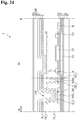
- the pixel electrode may further comprise a lower film under the reflective film, wherein the lower film comprises any one of ITO, IZO, ZnO, ITZO, and MgO.
- the first conductive layer may further comprise a low potential power supply voltage line
- the planarization layer comprises a second contact hole which partially exposes the low potential power supply voltage line
- the auxiliary line is electrically connected to the low potential power supply voltage line through the second contact hole.
- the sub low potential voltage lines SVSSL may pass the first pixels PX1, but may not pass the second pixels PX2 and the third pixels PX3. However, the present disclosure is not limited to this case, and the sub low potential voltage lines SVSSL may also be respectively located in the first through third pixels PX1 through PX3 emitting light of different colors.
- the timing controller 320 receives the digital video data DATA and timing signals from a host system. In addition, the timing controller 320 generates control signals for controlling operation timings of the data driver 310 and the scan driver 400.
- the control signals may include the source control signal DCS for controlling the operation timing of the data driver 310 and a scan control signal SCS for controlling the operation timing of the scan driver 400.
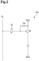
- the driving transistor DT may include the gate electrode connected to a source electrode of the scan transistor ST, the source electrode connected to the high potential voltage line VDDL to which the high potential voltage VDD is applied, and a drain electrode connected to the pixel electrodes of the organic light emitting elements LD.
- the scan transistor ST may include the gate electrode connected to a scan line SL, the source electrode connected to the gate electrode of the driving transistor DT, and the drain electrode connected to a data line DL.
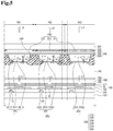
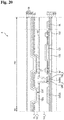
- a source/drain conductive layer may be arranged on the third insulating layer 113.
- the source/drain conductive layer may include a sub low potential voltage line SVSSL, a sub high potential voltage line SVDDL, a drain electrode 141 and a source electrode 142 of the thin-film transistor TFT, and a data line DL.
- the drain electrode 141 and the source electrode 142 of the thin-film transistor TFT may respectively be electrically connected to a drain region and a source region of the semiconductor layer 105 through contact holes passing through the third insulating layer 113, the second insulating layer 112 and the first insulating layer 111.
- the sub low potential voltage line SVSSL, the sub high potential voltage line SVDDL, and the drain electrode 141 and the source electrode 142 of the thin-film transistor TFT are spaced apart from each other.
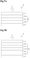
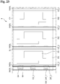
- Color filters 230 may be arranged on the surface of the second base substrate 201.
- the color filters 230 may include first through third color filters 231 through 233.
- the color filters 231 through 233 may be arranged in the pixels PX1 through PX3, respectively.
- Each of the first through third color filters 231 through 233 may be an absorptive filter that absorbs light of a specific wavelength and transmits light of another specific wavelength.
- the light transmission pattern 253 located in the third pixel PX3 may transmit the incident blue light L1 as it is.
- a filler 700 may be arranged between the light providing unit 100 and the light converting unit 200.
- the filler 700 may contact the thin-film encapsulation layer 180 of the light providing unit 100 and contact the third capping layer 243 and the second light shielding patterns 260 of the light converting unit 200.
- the filler 700 may planarize a surface step formed by the light conversion patterns 251 through 253 and the second light shielding patterns 260.
- the filler 700 may be made of a material having a buffer function and serve as a buffer member that absorbs shocks generated between the light providing unit 100 and the light converting unit 200.
- the filler 700 may be made of a silicon-based organic material, an epoxy-based organic material, or an acrylic-based organic material.
- the reflectance when the reflective film 153 according to the embodiment is applied, the reflectance may be about 80% or more over the entire wavelength range (about 420 nm to about 470 nm) of blue light.
- the pixel electrode 151 having an aluminium-nickel-alloy (AlNiX) as the reflective film 153 is illustrated.
- the average reflectance of light L R reflected upward by the pixel electrode 151 among the light L i provided toward the pixel electrode 151 is within the range of about 80% to about 90% over the entire wavelength range of blue light.
- the auxiliary line 152a may be arranged on the same layer as pixel electrodes 151 and spaced apart from the pixel electrodes 151. That is, the auxiliary line 152a may be electrically isolated from the pixel electrodes 151.
- the auxiliary line 152a may include the same material as the pixel electrodes 151.
Landscapes
- Engineering & Computer Science (AREA)
- Microelectronics & Electronic Packaging (AREA)
- Physics & Mathematics (AREA)
- Optics & Photonics (AREA)
- Electroluminescent Light Sources (AREA)
- Devices For Indicating Variable Information By Combining Individual Elements (AREA)
Applications Claiming Priority (1)
| Application Number | Priority Date | Filing Date | Title |
|---|---|---|---|
| KR1020180158026A KR102612713B1 (ko) | 2018-12-10 | 2018-12-10 | 표시 장치 |
Publications (2)
| Publication Number | Publication Date |
|---|---|
| EP3667754A1 true EP3667754A1 (de) | 2020-06-17 |
| EP3667754B1 EP3667754B1 (de) | 2022-10-12 |
Family
ID=68848139
Family Applications (1)
| Application Number | Title | Priority Date | Filing Date |
|---|---|---|---|
| EP19214987.0A Active EP3667754B1 (de) | 2018-12-10 | 2019-12-10 | Anzeigevorrichtung |
Country Status (4)
| Country | Link |
|---|---|
| US (1) | US11056667B2 (de) |
| EP (1) | EP3667754B1 (de) |
| KR (1) | KR102612713B1 (de) |
| CN (1) | CN111293146B (de) |
Cited By (1)
| Publication number | Priority date | Publication date | Assignee | Title |
|---|---|---|---|---|
| EP3843154A1 (de) * | 2019-12-24 | 2021-06-30 | InnoLux Corporation | Anzeigevorrichtung |
Families Citing this family (19)
| Publication number | Priority date | Publication date | Assignee | Title |
|---|---|---|---|---|
| JP2016081562A (ja) * | 2014-10-09 | 2016-05-16 | ソニー株式会社 | 表示装置、表示装置の製造方法および電子機器 |
| KR102678994B1 (ko) * | 2019-07-03 | 2024-07-01 | 한국전자통신연구원 | 표시 장치 및 그 제조 방법 |
| KR102870085B1 (ko) | 2019-10-11 | 2025-10-17 | 삼성디스플레이 주식회사 | 색 변환 기판, 이를 포함하는 표시 장치 및 그 제조 방법 |
| KR102730925B1 (ko) * | 2019-12-31 | 2024-11-14 | 엘지디스플레이 주식회사 | 발광표시패널 및 이를 이용한 발광표시장치 |
| CN111505866B (zh) * | 2020-04-21 | 2022-04-12 | 京东方科技集团股份有限公司 | 显示装置及其制作方法 |
| KR102934061B1 (ko) * | 2020-05-12 | 2026-03-04 | 삼성디스플레이 주식회사 | 디스플레이 장치 |
| KR102734419B1 (ko) | 2020-07-03 | 2024-11-26 | 삼성디스플레이 주식회사 | 표시 장치 |
| KR102845502B1 (ko) * | 2020-07-14 | 2025-08-13 | 삼성디스플레이 주식회사 | 표시 패널 |
| KR102894490B1 (ko) * | 2020-07-22 | 2025-12-03 | 삼성디스플레이 주식회사 | 색 변환 기판 및 이를 포함하는 표시 장치 |
| KR102925876B1 (ko) * | 2020-09-17 | 2026-02-10 | 삼성디스플레이 주식회사 | 디스플레이 장치 및 그 제조방법 |
| CN114787699B (zh) * | 2020-09-29 | 2023-10-20 | 京东方科技集团股份有限公司 | 显示面板、显示设备、显示面板的制造方法以及对置基板 |
| KR20220060078A (ko) * | 2020-11-03 | 2022-05-11 | 삼성디스플레이 주식회사 | 표시 장치 |
| CN112382733A (zh) * | 2020-11-16 | 2021-02-19 | 京东方科技集团股份有限公司 | 一种柔性显示面板、柔性显示装置以及制作方法 |
| KR20220080923A (ko) * | 2020-12-08 | 2022-06-15 | 엘지디스플레이 주식회사 | 전계 발광 표시장치 |
| KR102903021B1 (ko) * | 2020-12-31 | 2025-12-22 | 삼성디스플레이 주식회사 | 표시 패널, 이를 구비한 표시 장치, 및 표시 패널의 제조방법 |
| KR20220099595A (ko) * | 2021-01-06 | 2022-07-14 | 삼성디스플레이 주식회사 | 표시 장치 |
| CN113745288A (zh) * | 2021-08-18 | 2021-12-03 | Tcl华星光电技术有限公司 | 显示面板及其制备方法 |
| KR20240011919A (ko) * | 2022-07-19 | 2024-01-29 | 삼성디스플레이 주식회사 | 표시장치 및 이의 제조방법 |
| KR20240038177A (ko) * | 2022-09-15 | 2024-03-25 | 삼성디스플레이 주식회사 | 색변환 기판 및 이를 포함하는 표시 장치의 제조 방법 |
Citations (5)
| Publication number | Priority date | Publication date | Assignee | Title |
|---|---|---|---|---|
| EP1587154A2 (de) * | 2004-02-14 | 2005-10-19 | Samsung SDI Co., Ltd. | Organische elektrolumineszente Anzeigevorrichtung und Verfahren zu deren Herstellung |
| EP1601031A1 (de) * | 2004-05-28 | 2005-11-30 | Samsung SDI Co., Ltd. | Organisches lichtemittierendes Bauelement und dessen Herstellung |
| JP2011033834A (ja) * | 2009-07-31 | 2011-02-17 | Kobe Steel Ltd | 表示装置の製造方法 |
| US20150250038A1 (en) * | 2014-02-28 | 2015-09-03 | Semiconductor Energy Laboratory Co., Ltd. | Method for manufacturing display device and method for manufacturing electronic device |
| KR20160080489A (ko) * | 2014-12-29 | 2016-07-08 | 엘지디스플레이 주식회사 | 유기발광표시장치의 화소 및 이의 동작방법 |
Family Cites Families (12)
| Publication number | Priority date | Publication date | Assignee | Title |
|---|---|---|---|---|
| JP2006301089A (ja) * | 2005-04-18 | 2006-11-02 | Toshiba Matsushita Display Technology Co Ltd | 液晶表示装置およびその製造方法 |
| KR100787461B1 (ko) * | 2006-11-10 | 2007-12-26 | 삼성에스디아이 주식회사 | 다층 구조의 애노드를 채용한 유기 발광 디스플레이 장치 |
| KR100964227B1 (ko) * | 2008-05-06 | 2010-06-17 | 삼성모바일디스플레이주식회사 | 평판 표시 장치용 박막 트랜지스터 어레이 기판, 이를포함하는 유기 발광 표시 장치, 및 이들의 제조 방법 |
| KR101976133B1 (ko) | 2012-11-20 | 2019-05-08 | 삼성디스플레이 주식회사 | 표시 장치 |
| KR102346262B1 (ko) * | 2014-07-14 | 2022-01-03 | 엘지디스플레이 주식회사 | 유기 발광 표시장치 및 이를 제조하는 방법 |
| KR101723880B1 (ko) * | 2015-08-31 | 2017-04-07 | 엘지디스플레이 주식회사 | 유기발광다이오드 표시장치 및 그의 제조 방법 |
| CN105932166B (zh) | 2016-05-03 | 2018-03-30 | 深圳市华星光电技术有限公司 | 自发光型显示装置及其制作方法 |
| TWI724063B (zh) * | 2016-06-24 | 2021-04-11 | 日商半導體能源研究所股份有限公司 | 顯示裝置、輸入輸出裝置、半導體裝置 |
| KR101878186B1 (ko) * | 2016-07-29 | 2018-08-17 | 엘지디스플레이 주식회사 | 유기 발광 표시 장치 및 그 제조 방법 |
| KR102701733B1 (ko) | 2016-09-30 | 2024-09-02 | 엘지디스플레이 주식회사 | 컬러필터 어레이 기판 및 이를 포함하는 유기발광 표시장치 |
| KR101980781B1 (ko) * | 2016-10-31 | 2019-05-21 | 엘지디스플레이 주식회사 | 유기 발광 표시 장치 및 그 제조 방법 |
| KR102924227B1 (ko) | 2016-12-28 | 2026-02-05 | 엘지디스플레이 주식회사 | 유기발광다이오드 표시장치 |
-
2018
- 2018-12-10 KR KR1020180158026A patent/KR102612713B1/ko active Active
-
2019
- 2019-11-26 US US16/695,833 patent/US11056667B2/en active Active
- 2019-12-10 EP EP19214987.0A patent/EP3667754B1/de active Active
- 2019-12-10 CN CN201911254969.0A patent/CN111293146B/zh active Active
Patent Citations (5)
| Publication number | Priority date | Publication date | Assignee | Title |
|---|---|---|---|---|
| EP1587154A2 (de) * | 2004-02-14 | 2005-10-19 | Samsung SDI Co., Ltd. | Organische elektrolumineszente Anzeigevorrichtung und Verfahren zu deren Herstellung |
| EP1601031A1 (de) * | 2004-05-28 | 2005-11-30 | Samsung SDI Co., Ltd. | Organisches lichtemittierendes Bauelement und dessen Herstellung |
| JP2011033834A (ja) * | 2009-07-31 | 2011-02-17 | Kobe Steel Ltd | 表示装置の製造方法 |
| US20150250038A1 (en) * | 2014-02-28 | 2015-09-03 | Semiconductor Energy Laboratory Co., Ltd. | Method for manufacturing display device and method for manufacturing electronic device |
| KR20160080489A (ko) * | 2014-12-29 | 2016-07-08 | 엘지디스플레이 주식회사 | 유기발광표시장치의 화소 및 이의 동작방법 |
Cited By (2)
| Publication number | Priority date | Publication date | Assignee | Title |
|---|---|---|---|---|
| EP3843154A1 (de) * | 2019-12-24 | 2021-06-30 | InnoLux Corporation | Anzeigevorrichtung |
| US11626460B2 (en) | 2019-12-24 | 2023-04-11 | Innolux Corporation | Display device including blue organic light emitting diode and blue light blocking layer |
Also Published As
| Publication number | Publication date |
|---|---|
| KR102612713B1 (ko) | 2023-12-12 |
| CN111293146A (zh) | 2020-06-16 |
| EP3667754B1 (de) | 2022-10-12 |
| CN111293146B (zh) | 2025-06-03 |
| US11056667B2 (en) | 2021-07-06 |
| KR20200071168A (ko) | 2020-06-19 |
| US20200185638A1 (en) | 2020-06-11 |
Similar Documents
| Publication | Publication Date | Title |
|---|---|---|
| EP3667754B1 (de) | Anzeigevorrichtung | |
| EP3503238B1 (de) | Anzeigevorrichtung | |
| CN111354304B (zh) | 显示装置 | |
| US11574985B2 (en) | Organic light-emitting diode display device and method of manufacturing same | |
| KR102023945B1 (ko) | 플렉서블 유기발광 디스플레이 장치 | |
| US10566407B2 (en) | Organic light emitting diode display having barrier layer on auxiliary electrode | |
| CN110890401A (zh) | 显示装置 | |
| CN111326673B (zh) | 显示装置 | |
| US11678500B2 (en) | Organic light emitting diode display device having conductive layer, conductive fill material and conductive black matrix | |
| US10535724B2 (en) | Organic light emitting diode display | |
| US12284862B2 (en) | Transparent display device | |
| KR20210081944A (ko) | 유기 발광 표시 장치 | |
| KR102609507B1 (ko) | 백색광 발광장치 및 이를 이용한 하이브리드 표시장치 | |
| CN113130566B (zh) | 有机发光二极管显示装置 | |
| KR102665677B1 (ko) | 유기발광 표시장치 | |
| KR102417452B1 (ko) | 표시장치 | |
| KR20210081946A (ko) | 유기 발광 표시 장치 | |
| KR20210067513A (ko) | 유기 발광 표시 장치 | |
| US20250351672A1 (en) | Display device | |
| US20250318386A1 (en) | Display device | |
| EP4604703A1 (de) | Anzeigevorrichtung und herstellungsverfahren dafür | |
| US20250221213A1 (en) | Transparent display device | |
| CN121358139A (zh) | 显示装置 | |
| CN118412365A (zh) | 显示装置 | |
| KR20240104754A (ko) | 발광 표시 장치 |
Legal Events
| Date | Code | Title | Description |
|---|---|---|---|
| PUAI | Public reference made under article 153(3) epc to a published international application that has entered the european phase |
Free format text: ORIGINAL CODE: 0009012 |
|
| STAA | Information on the status of an ep patent application or granted ep patent |
Free format text: STATUS: THE APPLICATION HAS BEEN PUBLISHED |
|
| AK | Designated contracting states |
Kind code of ref document: A1 Designated state(s): AL AT BE BG CH CY CZ DE DK EE ES FI FR GB GR HR HU IE IS IT LI LT LU LV MC MK MT NL NO PL PT RO RS SE SI SK SM TR |
|
| AX | Request for extension of the european patent |
Extension state: BA ME |
|
| STAA | Information on the status of an ep patent application or granted ep patent |
Free format text: STATUS: REQUEST FOR EXAMINATION WAS MADE |
|
| 17P | Request for examination filed |
Effective date: 20201216 |
|
| RBV | Designated contracting states (corrected) |
Designated state(s): AL AT BE BG CH CY CZ DE DK EE ES FI FR GB GR HR HU IE IS IT LI LT LU LV MC MK MT NL NO PL PT RO RS SE SI SK SM TR |
|
| GRAP | Despatch of communication of intention to grant a patent |
Free format text: ORIGINAL CODE: EPIDOSNIGR1 |
|
| STAA | Information on the status of an ep patent application or granted ep patent |
Free format text: STATUS: GRANT OF PATENT IS INTENDED |
|
| INTG | Intention to grant announced |
Effective date: 20220517 |
|
| GRAS | Grant fee paid |
Free format text: ORIGINAL CODE: EPIDOSNIGR3 |
|
| GRAA | (expected) grant |
Free format text: ORIGINAL CODE: 0009210 |
|
| STAA | Information on the status of an ep patent application or granted ep patent |
Free format text: STATUS: THE PATENT HAS BEEN GRANTED |
|
| AK | Designated contracting states |
Kind code of ref document: B1 Designated state(s): AL AT BE BG CH CY CZ DE DK EE ES FI FR GB GR HR HU IE IS IT LI LT LU LV MC MK MT NL NO PL PT RO RS SE SI SK SM TR |
|
| REG | Reference to a national code |
Ref country code: GB Ref legal event code: FG4D |
|
| REG | Reference to a national code |
Ref country code: CH Ref legal event code: EP |
|
| REG | Reference to a national code |
Ref country code: DE Ref legal event code: R096 Ref document number: 602019020498 Country of ref document: DE |
|
| REG | Reference to a national code |
Ref country code: IE Ref legal event code: FG4D |
|
| REG | Reference to a national code |
Ref country code: AT Ref legal event code: REF Ref document number: 1524705 Country of ref document: AT Kind code of ref document: T Effective date: 20221115 |
|
| REG | Reference to a national code |
Ref country code: DE Ref legal event code: R079 Ref document number: 602019020498 Country of ref document: DE Free format text: PREVIOUS MAIN CLASS: H01L0051520000 Ipc: H10K0050800000 |
|
| REG | Reference to a national code |
Ref country code: LT Ref legal event code: MG9D |
|
| REG | Reference to a national code |
Ref country code: NL Ref legal event code: MP Effective date: 20221012 |
|
| REG | Reference to a national code |
Ref country code: AT Ref legal event code: MK05 Ref document number: 1524705 Country of ref document: AT Kind code of ref document: T Effective date: 20221012 |
|
| PG25 | Lapsed in a contracting state [announced via postgrant information from national office to epo] |
Ref country code: NL Free format text: LAPSE BECAUSE OF FAILURE TO SUBMIT A TRANSLATION OF THE DESCRIPTION OR TO PAY THE FEE WITHIN THE PRESCRIBED TIME-LIMIT Effective date: 20221012 |
|
| PG25 | Lapsed in a contracting state [announced via postgrant information from national office to epo] |
Ref country code: SE Free format text: LAPSE BECAUSE OF FAILURE TO SUBMIT A TRANSLATION OF THE DESCRIPTION OR TO PAY THE FEE WITHIN THE PRESCRIBED TIME-LIMIT Effective date: 20221012 Ref country code: PT Free format text: LAPSE BECAUSE OF FAILURE TO SUBMIT A TRANSLATION OF THE DESCRIPTION OR TO PAY THE FEE WITHIN THE PRESCRIBED TIME-LIMIT Effective date: 20230213 Ref country code: NO Free format text: LAPSE BECAUSE OF FAILURE TO SUBMIT A TRANSLATION OF THE DESCRIPTION OR TO PAY THE FEE WITHIN THE PRESCRIBED TIME-LIMIT Effective date: 20230112 Ref country code: LT Free format text: LAPSE BECAUSE OF FAILURE TO SUBMIT A TRANSLATION OF THE DESCRIPTION OR TO PAY THE FEE WITHIN THE PRESCRIBED TIME-LIMIT Effective date: 20221012 Ref country code: FI Free format text: LAPSE BECAUSE OF FAILURE TO SUBMIT A TRANSLATION OF THE DESCRIPTION OR TO PAY THE FEE WITHIN THE PRESCRIBED TIME-LIMIT Effective date: 20221012 Ref country code: ES Free format text: LAPSE BECAUSE OF FAILURE TO SUBMIT A TRANSLATION OF THE DESCRIPTION OR TO PAY THE FEE WITHIN THE PRESCRIBED TIME-LIMIT Effective date: 20221012 Ref country code: AT Free format text: LAPSE BECAUSE OF FAILURE TO SUBMIT A TRANSLATION OF THE DESCRIPTION OR TO PAY THE FEE WITHIN THE PRESCRIBED TIME-LIMIT Effective date: 20221012 |
|
| PG25 | Lapsed in a contracting state [announced via postgrant information from national office to epo] |
Ref country code: RS Free format text: LAPSE BECAUSE OF FAILURE TO SUBMIT A TRANSLATION OF THE DESCRIPTION OR TO PAY THE FEE WITHIN THE PRESCRIBED TIME-LIMIT Effective date: 20221012 Ref country code: PL Free format text: LAPSE BECAUSE OF FAILURE TO SUBMIT A TRANSLATION OF THE DESCRIPTION OR TO PAY THE FEE WITHIN THE PRESCRIBED TIME-LIMIT Effective date: 20221012 Ref country code: LV Free format text: LAPSE BECAUSE OF FAILURE TO SUBMIT A TRANSLATION OF THE DESCRIPTION OR TO PAY THE FEE WITHIN THE PRESCRIBED TIME-LIMIT Effective date: 20221012 Ref country code: IS Free format text: LAPSE BECAUSE OF FAILURE TO SUBMIT A TRANSLATION OF THE DESCRIPTION OR TO PAY THE FEE WITHIN THE PRESCRIBED TIME-LIMIT Effective date: 20230212 Ref country code: HR Free format text: LAPSE BECAUSE OF FAILURE TO SUBMIT A TRANSLATION OF THE DESCRIPTION OR TO PAY THE FEE WITHIN THE PRESCRIBED TIME-LIMIT Effective date: 20221012 Ref country code: GR Free format text: LAPSE BECAUSE OF FAILURE TO SUBMIT A TRANSLATION OF THE DESCRIPTION OR TO PAY THE FEE WITHIN THE PRESCRIBED TIME-LIMIT Effective date: 20230113 |
|
| P01 | Opt-out of the competence of the unified patent court (upc) registered |
Effective date: 20230516 |
|
| REG | Reference to a national code |
Ref country code: DE Ref legal event code: R097 Ref document number: 602019020498 Country of ref document: DE |
|
| PG25 | Lapsed in a contracting state [announced via postgrant information from national office to epo] |
Ref country code: SM Free format text: LAPSE BECAUSE OF FAILURE TO SUBMIT A TRANSLATION OF THE DESCRIPTION OR TO PAY THE FEE WITHIN THE PRESCRIBED TIME-LIMIT Effective date: 20221012 Ref country code: RO Free format text: LAPSE BECAUSE OF FAILURE TO SUBMIT A TRANSLATION OF THE DESCRIPTION OR TO PAY THE FEE WITHIN THE PRESCRIBED TIME-LIMIT Effective date: 20221012 Ref country code: EE Free format text: LAPSE BECAUSE OF FAILURE TO SUBMIT A TRANSLATION OF THE DESCRIPTION OR TO PAY THE FEE WITHIN THE PRESCRIBED TIME-LIMIT Effective date: 20221012 Ref country code: DK Free format text: LAPSE BECAUSE OF FAILURE TO SUBMIT A TRANSLATION OF THE DESCRIPTION OR TO PAY THE FEE WITHIN THE PRESCRIBED TIME-LIMIT Effective date: 20221012 Ref country code: CZ Free format text: LAPSE BECAUSE OF FAILURE TO SUBMIT A TRANSLATION OF THE DESCRIPTION OR TO PAY THE FEE WITHIN THE PRESCRIBED TIME-LIMIT Effective date: 20221012 |
|
| REG | Reference to a national code |
Ref country code: CH Ref legal event code: PL |
|
| PLBE | No opposition filed within time limit |
Free format text: ORIGINAL CODE: 0009261 |
|
| STAA | Information on the status of an ep patent application or granted ep patent |
Free format text: STATUS: NO OPPOSITION FILED WITHIN TIME LIMIT |
|
| REG | Reference to a national code |
Ref country code: BE Ref legal event code: MM Effective date: 20221231 |
|
| PG25 | Lapsed in a contracting state [announced via postgrant information from national office to epo] |
Ref country code: SK Free format text: LAPSE BECAUSE OF FAILURE TO SUBMIT A TRANSLATION OF THE DESCRIPTION OR TO PAY THE FEE WITHIN THE PRESCRIBED TIME-LIMIT Effective date: 20221012 Ref country code: LU Free format text: LAPSE BECAUSE OF NON-PAYMENT OF DUE FEES Effective date: 20221210 Ref country code: AL Free format text: LAPSE BECAUSE OF FAILURE TO SUBMIT A TRANSLATION OF THE DESCRIPTION OR TO PAY THE FEE WITHIN THE PRESCRIBED TIME-LIMIT Effective date: 20221012 |
|
| 26N | No opposition filed |
Effective date: 20230713 |
|
| PG25 | Lapsed in a contracting state [announced via postgrant information from national office to epo] |
Ref country code: LI Free format text: LAPSE BECAUSE OF NON-PAYMENT OF DUE FEES Effective date: 20221231 Ref country code: IE Free format text: LAPSE BECAUSE OF NON-PAYMENT OF DUE FEES Effective date: 20221210 Ref country code: CH Free format text: LAPSE BECAUSE OF NON-PAYMENT OF DUE FEES Effective date: 20221231 |
|
| PG25 | Lapsed in a contracting state [announced via postgrant information from national office to epo] |
Ref country code: SI Free format text: LAPSE BECAUSE OF FAILURE TO SUBMIT A TRANSLATION OF THE DESCRIPTION OR TO PAY THE FEE WITHIN THE PRESCRIBED TIME-LIMIT Effective date: 20221012 Ref country code: BE Free format text: LAPSE BECAUSE OF NON-PAYMENT OF DUE FEES Effective date: 20221231 |
|
| PG25 | Lapsed in a contracting state [announced via postgrant information from national office to epo] |
Ref country code: HU Free format text: LAPSE BECAUSE OF FAILURE TO SUBMIT A TRANSLATION OF THE DESCRIPTION OR TO PAY THE FEE WITHIN THE PRESCRIBED TIME-LIMIT; INVALID AB INITIO Effective date: 20191210 |
|
| PG25 | Lapsed in a contracting state [announced via postgrant information from national office to epo] |
Ref country code: CY Free format text: LAPSE BECAUSE OF FAILURE TO SUBMIT A TRANSLATION OF THE DESCRIPTION OR TO PAY THE FEE WITHIN THE PRESCRIBED TIME-LIMIT Effective date: 20221012 |
|
| PG25 | Lapsed in a contracting state [announced via postgrant information from national office to epo] |
Ref country code: MK Free format text: LAPSE BECAUSE OF FAILURE TO SUBMIT A TRANSLATION OF THE DESCRIPTION OR TO PAY THE FEE WITHIN THE PRESCRIBED TIME-LIMIT Effective date: 20221012 Ref country code: IT Free format text: LAPSE BECAUSE OF FAILURE TO SUBMIT A TRANSLATION OF THE DESCRIPTION OR TO PAY THE FEE WITHIN THE PRESCRIBED TIME-LIMIT Effective date: 20221012 |
|
| PG25 | Lapsed in a contracting state [announced via postgrant information from national office to epo] |
Ref country code: MC Free format text: LAPSE BECAUSE OF FAILURE TO SUBMIT A TRANSLATION OF THE DESCRIPTION OR TO PAY THE FEE WITHIN THE PRESCRIBED TIME-LIMIT Effective date: 20221012 |
|
| PG25 | Lapsed in a contracting state [announced via postgrant information from national office to epo] |
Ref country code: MC Free format text: LAPSE BECAUSE OF FAILURE TO SUBMIT A TRANSLATION OF THE DESCRIPTION OR TO PAY THE FEE WITHIN THE PRESCRIBED TIME-LIMIT Effective date: 20221012 |
|
| PG25 | Lapsed in a contracting state [announced via postgrant information from national office to epo] |
Ref country code: BG Free format text: LAPSE BECAUSE OF FAILURE TO SUBMIT A TRANSLATION OF THE DESCRIPTION OR TO PAY THE FEE WITHIN THE PRESCRIBED TIME-LIMIT Effective date: 20221012 |
|
| PG25 | Lapsed in a contracting state [announced via postgrant information from national office to epo] |
Ref country code: MT Free format text: LAPSE BECAUSE OF FAILURE TO SUBMIT A TRANSLATION OF THE DESCRIPTION OR TO PAY THE FEE WITHIN THE PRESCRIBED TIME-LIMIT Effective date: 20221012 |
|
| PG25 | Lapsed in a contracting state [announced via postgrant information from national office to epo] |
Ref country code: TR Free format text: LAPSE BECAUSE OF FAILURE TO SUBMIT A TRANSLATION OF THE DESCRIPTION OR TO PAY THE FEE WITHIN THE PRESCRIBED TIME-LIMIT Effective date: 20221012 |
|
| PGFP | Annual fee paid to national office [announced via postgrant information from national office to epo] |
Ref country code: DE Payment date: 20251120 Year of fee payment: 7 |
|
| PGFP | Annual fee paid to national office [announced via postgrant information from national office to epo] |
Ref country code: GB Payment date: 20251120 Year of fee payment: 7 |
|
| PGFP | Annual fee paid to national office [announced via postgrant information from national office to epo] |
Ref country code: FR Payment date: 20251125 Year of fee payment: 7 |