EP3667892A1 - Dispositif de conversion de puissance et procédé de refroidissement associé - Google Patents
Dispositif de conversion de puissance et procédé de refroidissement associé Download PDFInfo
- Publication number
- EP3667892A1 EP3667892A1 EP18844422.8A EP18844422A EP3667892A1 EP 3667892 A1 EP3667892 A1 EP 3667892A1 EP 18844422 A EP18844422 A EP 18844422A EP 3667892 A1 EP3667892 A1 EP 3667892A1
- Authority
- EP
- European Patent Office
- Prior art keywords
- electric
- gate drive
- power conversion
- drive device
- conversion device
- Prior art date
- Legal status (The legal status is an assumption and is not a legal conclusion. Google has not performed a legal analysis and makes no representation as to the accuracy of the status listed.)
- Withdrawn
Links
Images


Classifications
-
- H—ELECTRICITY
- H02—GENERATION; CONVERSION OR DISTRIBUTION OF ELECTRIC POWER
- H02M—APPARATUS FOR CONVERSION BETWEEN AC AND AC, BETWEEN AC AND DC, OR BETWEEN DC AND DC, AND FOR USE WITH MAINS OR SIMILAR POWER SUPPLY SYSTEMS; CONVERSION OF DC OR AC INPUT POWER INTO SURGE OUTPUT POWER; CONTROL OR REGULATION THEREOF
- H02M7/00—Conversion of AC power input into DC power output; Conversion of DC power input into AC power output
- H02M7/003—Constructional details, e.g. physical layout, assembly, wiring or busbar connections
-
- H—ELECTRICITY
- H02—GENERATION; CONVERSION OR DISTRIBUTION OF ELECTRIC POWER
- H02M—APPARATUS FOR CONVERSION BETWEEN AC AND AC, BETWEEN AC AND DC, OR BETWEEN DC AND DC, AND FOR USE WITH MAINS OR SIMILAR POWER SUPPLY SYSTEMS; CONVERSION OF DC OR AC INPUT POWER INTO SURGE OUTPUT POWER; CONTROL OR REGULATION THEREOF
- H02M1/00—Details of apparatus for conversion
- H02M1/08—Circuits specially adapted for the generation of control voltages for semiconductor devices incorporated in static converters
-
- H—ELECTRICITY
- H05—ELECTRIC TECHNIQUES NOT OTHERWISE PROVIDED FOR
- H05K—PRINTED CIRCUITS; CASINGS OR CONSTRUCTIONAL DETAILS OF ELECTRIC APPARATUS; MANUFACTURE OF ASSEMBLAGES OF ELECTRICAL COMPONENTS
- H05K7/00—Constructional details common to different types of electric apparatus
- H05K7/14—Mounting supporting structure in casing or on frame or rack
- H05K7/1422—Printed circuit boards receptacles, e.g. stacked structures, electronic circuit modules or box like frames
- H05K7/1427—Housings
- H05K7/1432—Housings specially adapted for power drive units or power converters
- H05K7/14325—Housings specially adapted for power drive units or power converters for cabinets or racks
-
- H—ELECTRICITY
- H05—ELECTRIC TECHNIQUES NOT OTHERWISE PROVIDED FOR
- H05K—PRINTED CIRCUITS; CASINGS OR CONSTRUCTIONAL DETAILS OF ELECTRIC APPARATUS; MANUFACTURE OF ASSEMBLAGES OF ELECTRICAL COMPONENTS
- H05K7/00—Constructional details common to different types of electric apparatus
- H05K7/20—Modifications to facilitate cooling, ventilating, or heating
- H05K7/2089—Modifications to facilitate cooling, ventilating, or heating for power electronics, e.g. for inverters for controlling motor
- H05K7/20927—Liquid coolant without phase change
-
- H—ELECTRICITY
- H03—ELECTRONIC CIRCUITRY
- H03K—PULSE TECHNIQUE
- H03K17/00—Electronic switching or gating, i.e. not by contact-making and –breaking
- H03K17/08—Modifications for protecting switching circuit against overcurrent or overvoltage
- H03K2017/0806—Modifications for protecting switching circuit against overcurrent or overvoltage against excessive temperature
-
- H—ELECTRICITY
- H10—SEMICONDUCTOR DEVICES; ELECTRIC SOLID-STATE DEVICES NOT OTHERWISE PROVIDED FOR
- H10W—GENERIC PACKAGES, INTERCONNECTIONS, CONNECTORS OR OTHER CONSTRUCTIONAL DETAILS OF DEVICES COVERED BY CLASS H10
- H10W40/00—Arrangements for thermal protection or thermal control
- H10W40/40—Arrangements for thermal protection or thermal control involving heat exchange by flowing fluids
- H10W40/43—Arrangements for thermal protection or thermal control involving heat exchange by flowing fluids by flowing gases, e.g. forced air cooling
Definitions
- the present invention relates to an electric-power conversion device on which a power semiconductor module is loaded and a cooling method therefor.
- An electric-power conversion device for railroad vehicle which is installed on the railroad vehicle is the one which subjects electric power which is input from a railroad overhead wire to electric-power conversion by a switching operation of a main circuit which is composed of a plurality of power semiconductor modules and controls an electric motor for railroad vehicle.
- the main circuit which is a main constitutional device of this electric-power conversion device is configured by the power semiconductor module which is a switching elements, a gate drive device which is a drive circuit thereof, a filter capacitor for stabilization of direct current electric power which is input from the overhead wire and so forth.
- miniaturization of the electric-power conversion device has been requested conventionally, and miniaturization of components themselves such as the power semiconductor module, the gate drive device, the filter capacitor and so forth is effective for realization of miniaturization thereof. Further miniaturization can be realized by efficiently arranging the components of the electric-power conversion device, in addition to this.
- the gate drive device there is the possibility in the gate drive device that an electronic component that it mounts thereon may induce problems of malfunction and life reduction due to thermal effect.
- the power semiconductor module, an electric wire cable and so forth generate heat themselves and therefore there is the possibility that the vicinity thereof may reach a high temperature, it is requested to arrange the gate drive device by avoiding the thermal effect from surrounding heat generation components.
- Patent Literature 1 An electric-power conversion device that miniaturization and arrangement of the gate drive device are taken into consideration is described in Patent Literature 1.
- a gate control circuit 7 is arranged on a lower-face part of an electric-power conversion unit 6, in a lower-face-part space of a filter capacitor 2, and on the front-face side (the opposite side of a cooling fin) in Fig. 1 ".
- Patent Literature 1 Japanese Patent Application Laid-Open No. 2010-284049
- the electric-power conversion device is configured by a casing, the power semiconductor module, the filter capacitor, a cooling block, and the gate drive device.
- the gate drive device is arranged on the gravity-direction lower side of the filter capacitor, taking that the gate drive device is used under a condition that the temperature of surrounding air is low into consideration as a conventional mounting system of the gate drive device.
- the gate drive devices are arranged even with the ground surface and laterally side by side.
- a small-sized electric-power conversion device in this equipment arrangement, it depends on the breath of the gate drive device and therefore a small-sized gate drive device was necessary.
- a subject of the present invention is to promote improvement of a heat radiation performance of the gate drive device and miniaturization of the electric-power conversion device.
- representative one of electric-power conversion devices of the present invention is equipped with a power semiconductor module which has a plurality of switching elements which configure an electric-power conversion circuit, a filter capacitor which smooths a direct current voltage which is applied to the electric-power conversion circuit, and one, two or more gate drive device(s) which send(s) a control signal(s) for controlling switching operations of the plurality of switching elements to the plurality of switching elements, in which the one, two or more gate drive device(s) is/are arranged perpendicularly to the ground surface.
- FIG. 1 A first embodiment of the present invention will be described by using Fig. 1 to Fig. 5 .
- Fig. 1 is a perspective diagram of the electric-power conversion device of the first embodiment.
- the present electric-power conversion device is configured by a casing 10, a power semiconductor module 1 (not illustrated), a filter capacitor 2, a cooling block 3, and a gate drive device 4, and is loaded on, for example, a vehicle body of a railroad vehicle.
- the casing 10 is configured into the box shape by using a frame-shaped frame body and is arranged on or under the vehicle body.
- a plurality of the filter capacitors 2, and the cooling block 3 are housed in its upper region, and a plurality of the gate drive devices 4 are housed in a lower region.
- the filter capacitors 2 are arranged with the cooling block 3 being interposed therebetween.
- the bottom sides of the cooling block 3 and each filter capacitor 2 are supported on a support frame 11 which is fixed to the casing 10.
- the respective gate drive devices 4 are arranged on the lower sides (the lower sides in a gravity acting direction) of the filter capacitors 2 and perpendicularly to the ground surface in the lower region in the casing 10.
- the respective gate drive devices 4 are arranged adjacently to each other/one another and are side by side in a lateral direction (the direction which intersects a rail) along the ground surface at regular intervals.
- a longitudinal direction of each gate drive devices 4 is arranged along the rail.
- a connector (not illustrated) which is an optical fiber connection terminal that a command signal from a control logic unit 40 (see Fig. 2 ) is input is arranged on each gate drive device 4 so as to expose to a front face of the casing 10. For this reason, attachment and detachment of the connector becomes easy.
- FIG. 2 is an electric circuit diagram of the electric-power conversion device of the first embodiment.
- the present electric-power conversion device is equipped with two sets of the electric-power conversion circuits.
- Each of the present electric-power conversion circuits outputs an alternate current voltage to M-pole wiring 5m with a direct current voltage which is applied between P-pole wiring 5p and N-pole wiring 5n being received as an input.
- the filter capacitor 2 which is adapted to smooth the direct current voltage is connected between the P-pole wiring 5p and the N-pole wiring 5n. Conversion from the direct current voltage to the alternate current voltage is realized by switching operations of a plurality of switching element which belong to each power semiconductor module 1.
- each power semiconductor module is equipped with one set of the electric-power conversion circuits, and this electric-power conversion circuit is configured by, for example, three sets (three pairs) of IGBTs (Insulated Gate Bipolar Transistor) 1A, 1B which are connected in series with one another, and freewheel diodes 1C, 1D which are connected in parallel between a collector and an emitter of each of the IGBTs 1A and 1B as the plurality of switching elements which configure a three-phase inverter.
- IGBTs Insulated Gate Bipolar Transistor
- a gate and the emitter of each of the IGBTs 1A, 1B are connected to each gate drive device 4 via gate wiring 5g and emitter wiring 5e respectively, and each of the IGBTs 1A, 1B receives a control signal from the gate drive device 4 and performs the switching operation. This switching operation is done in linkage with a gate voltage that each gate drive device 4 outputs.
- the gate voltage is generated by each gate drive device 4 on the basis of a command signal which is transmitted from the control logic unit 40 which is connected to each gate drive device 4.
- the present electric-power conversion device is not limited to the one which configures the two sets of the electric-power conversion circuits by one present electric-power conversion device, and may be the one which configures one set, three or more sets of the electric-power conversion circuits.
- FIG. 3 is a front view of the electric-power conversion device of the first embodiment.
- the cooling block 3 is arranged on a central part of an upper region in the casing 10, and the plurality of power semiconductor modules 1 are arranged on both side-faces of the cooling block 3.
- the filter capacitors 2 are arranged on the both sides of the cooling block 3 with space parts being maintained therebetween.
- a cooling water circulation passage (not illustrated) through which cooling water circulates is formed in the cooling block 3 in such manner that the plurality of switching elements (not illustrated) which belongs to each power semiconductor module 1 are cooled with the cooling water which circulates through the cooling block 3.
- the plurality of gate drive devices 4 having control circuits which generate control signals which are adapted to apply control signals to the respective switching elements (IGBTs), and a plurality of transformers 20 which are connected to the control circuits so as to, for example, boost the control signals are arranged in the region which is the lower region in the casing 10 and is under the support frame 11.
- Each gate drive device 4 is arranged on the lower side (the lower side in the gravity acting direction) of the filter capacitor 2 and perpendicularly to the ground surface in the lower region in the casing 10.
- each gate drive device 4 is arranged on the front-face side (the frontal side) which is more forward than each transformer 20 and is fixed to a gate drive fixing plate which is fixed to the casing via an L-shaped tray and a spacer (none of them are illustrated).
- Each transformer 20 is arranged on the back-face side which is more backward than each gate drive device 4 and is fixed to a transformer fixing plate 30 which is fixed to the casing 10. It becomes easy for air which is warmed by each gate drive device 4 to escape toward the upper side via the space part between the filter capacitor 2 and the cooling block 3 by arranging each gate drive device 4 perpendicularly to the ground surface.
- each gate drive device 4 can be cooled by introducing the air from the gravity-direction lower side (the bottom side of the casing 10) of each gate drive device 4 onto the gravity-direction upper side of each gate drive device 4. Thereby, it becomes easy to supply cold air to each gate drive device 4, and improvement of the heat radiation performance can be more promoted than in a case where each gate drive device 4 is arranged in a horizontal direction.
- heat transfer coefficients in a case where each gate drive device 4 is arranged horizontally and in a case where each gate drive device 4 is arranged vertically can be obtained from the following calculation formulae.
- the following calculation formulae are the ones which are generally defined and are not limited to the present invention.
- the heat transfer coefficient h can be obtained by the following calculation formulae (Numerical Formula 1 to Numerical formula 3).
- Nu 0.27
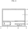
- Fig. 4 is a side view (the side view along the B-B line in Fig. 3 ) of the electric-power conversion device of the first embodiment.
- the plurality of gate drive devices 4 are arranged in one line in the region which is the lower region in the casing 10 and is under the support frame 11.
- the plurality of transformers 20 are arranged in two lines in the region which is the lower region in the casing 10 and is under the support frame 11. On this occasion, a space part is formed between each gate drive device 4 and each transformer 20.
- each gate drive device 4 of a light electricity system and each transformer 20 of a heavy electricity system are separately arranged.
- each gate drive device main body (the gate drive device 4 which builds the control circuit therein), and each transformer 20 are arranged separately from each other.
- the transformer 20 is high and therefore a spacing between the adjacent gate drive devices 4 cannot be narrowed.
- the transformer 20 itself generates heat, other pieces of equipment in the gate drive device 4 and the adjacent gate drive devices 4 are influenced by heat generation.
- each gate drive device 4 and each transformer 20 are arranged separately as in the present electric-power conversion device, each gate drive device 4 is not influenced by heat generation of each transformer 20 and can be arranged by narrowing the spacing between the adjacent gate drive devices 4.
- the connector which is adapted to perform command signal transmission and reception with the control logic unit 40 is arranged on the side-face side (the front-face side of the casing 10) of each gate drive device 4 as the connection terminal or a terminal part so as to be exposed to the outside of the casing 10.
- FIG. 5 is a bottom view (the bottom view along the C-C line in Fig. 4 ) of the electric-power conversion device of the first embodiment.
- the present electric-power conversion device is equipped with the transformer fixing plate 30 which has a ventilation hole for improvement of a cooling performance of the transformer 20 and transformer fixing hole 31.
- the plurality of gate drive devices 4 are arranged in one line, and the plurality of transformers 20 are arranged in two lines. On this occasion, the plurality of transformers 20 are arranged on the two transformer fixing plates 30 six by six.
- the ventilation holes for improvement of the cooling performance of the transformer 20 and transformer fixing holes 31 are plurally formed in each transformer fixing plate 30 over the entire surface thereof.
- the respective ventilation holes and transformer fixing holes 31 are formed in each transformer fixing plate 30 over the entire surface thereof in order to make it possible to freely change the arrangement of each transformer 20.
- each transformer 20 is connected with each gate drive device 4 by wiring, necessity to change an attachment position of any of the transformers 20 occurs depending on a length of the wiring and a route of the wiring.
- the present electric-power conversion device has the plurality of ventilation holes and transformer positioning holes 31, each transformer 20 can be arranged at an optional position on each transformer fixing plate 30 without being influenced by the length and the route of the wiring, and improvement of workability in attachment of the transformers 20 can be promoted.
- the present electric-power conversion device can dissipate the heat which is generated in each transformer 20 toward the upper side of each transformer 20 through the ventilation hole and transformer fixing hole 31, and thereby can promote improvement of the cooling performance of each transformer 20.
- the plurality of transformers 20 are dispersedly arranged in the hound's-tooth check form. Thereby, an attachment width of the plurality of transformers 20 can be suppressed, and the electric-power conversion device can be more miniaturized.
- the respective gate drive devices 4 are arranged on the lower side of the filter capacitor 2 and perpendicularly to the ground surface, and, further, the respective gate drive devices 4 are arranged adjacently to each other/one another and side by side in the lateral direction (the direction which intersects the rail) along the ground surface, a reduction in pressure loss, improvement of a travelling wind taking-in amount and improvement of the heat transfer coefficient can be promoted, and, as a result, improvement of the cooling performance and the life of each gate drive device 4 can be promoted.
- the switching element can be cooled with the cooling water which circulates through the cooling block 3.
- the semiconductor module 1 and the filter capacitor 2 are arranged on one side of the cooling block 3, and a cooling fin 6 is arranged on the other side unlike the first embodiment.
- description will be made with a focus on points which are different from those in the first embodiment.
- FIG. 6 is a perspective diagram of the electric-power conversion device of the second embodiment.
- the cooling block 3 is arranged on the back-face side in the casing 10, and a space part which is larger than that in the first embodiment is formed between the filter capacitor 2 and the filter capacitor 2.
- the plurality of power semiconductor modules 1 are fixed to the front-face side (one side) of the cooling block 3, and the cooling fin 6 which is exposed from the casing 10 to the outside of the vehicle body is fixed to the back-face side of the cooling block 3.
- the cooling fin 6 functions as a radiator which radiates heat of the power semiconductor module 1 (heat of the switching elements and so forth) to the atmosphere. On this occasion, the power semiconductor module 1 can be cooled by natural air-cooling via the cooling fin 6 without circulating the cooling water in the cooling block 3.
- Each gate drive device 4 is arranged on the gravity-direction lower side of the filter capacitor 2 and perpendicularly to the ground surface similarly to that in the first embodiment.
- the respective filter capacitors 2 are dividedly arranged on the left and the right in a case of viewing from the front-face side (an arrow view D in Fig. 6 ), the filter capacitors 2 may be formed as an integrated type one.
- the same effects as those of the first embodiment can be exhibited, and the power semiconductor module 1 can be cooled by natural air-cooling via the cooling fin 6.
- the cooling block 3 is arranged on the back-face side of the casing 10, and the space part which is larger than that in the first embodiment is formed between the filter capacitors 2, the heat radiation performance of each gate drive device 4 can be more heightened than that in the first embodiment.
- the present invention is not limited to the above-described embodiments and various modified examples are included.
- improvement of the heat radiation performance of the gate drive device 4 can be promoted, and the electric-power conversion device can be miniaturized by vertically arranging the gate drive device 4.
- the above-described embodiments are the ones which are described in detail for the purpose of comprehensively describing the present invention and it is not necessarily limited to the one which is equipped with all the configurations which have been described.
- 1 power semiconductor module 1 power semiconductor module, 2 filter capacitor, 3 cooling block, 4 gate drive device, 5p P-pole wiring, 5n N-pole wiring, 5m M-pole wiring, 5g gate wiring, 5e emitter wiring, 6 cooling fin, 10 casing, 11 support frame, 20 transformer, 30 transformer fixing plate, 31 ventilation hole and transformer fixing hole, 40 control logic unit
Landscapes
- Engineering & Computer Science (AREA)
- Microelectronics & Electronic Packaging (AREA)
- Power Engineering (AREA)
- Physics & Mathematics (AREA)
- Thermal Sciences (AREA)
- Inverter Devices (AREA)
- Cooling Or The Like Of Electrical Apparatus (AREA)
- Power Conversion In General (AREA)
- Electric Propulsion And Braking For Vehicles (AREA)
Applications Claiming Priority (2)
| Application Number | Priority Date | Filing Date | Title |
|---|---|---|---|
| JP2017154833 | 2017-08-09 | ||
| PCT/JP2018/012824 WO2019030968A1 (fr) | 2017-08-09 | 2018-03-28 | Dispositif de conversion de puissance et procédé de refroidissement associé |
Publications (2)
| Publication Number | Publication Date |
|---|---|
| EP3667892A1 true EP3667892A1 (fr) | 2020-06-17 |
| EP3667892A4 EP3667892A4 (fr) | 2021-04-07 |
Family
ID=65271448
Family Applications (1)
| Application Number | Title | Priority Date | Filing Date |
|---|---|---|---|
| EP18844422.8A Withdrawn EP3667892A4 (fr) | 2017-08-09 | 2018-03-28 | Dispositif de conversion de puissance et procédé de refroidissement associé |
Country Status (4)
| Country | Link |
|---|---|
| EP (1) | EP3667892A4 (fr) |
| JP (1) | JP6849807B2 (fr) |
| CN (1) | CN110959253A (fr) |
| WO (1) | WO2019030968A1 (fr) |
Families Citing this family (2)
| Publication number | Priority date | Publication date | Assignee | Title |
|---|---|---|---|---|
| CN115118124B (zh) * | 2022-06-08 | 2024-06-18 | 北京交通大学 | 一种交直流供电变换器功率模块 |
| PL444614A1 (pl) * | 2023-04-26 | 2024-10-28 | Triol-Poland Spółka Z Ograniczoną Odpowiedzialnością | Sposób obsługi kompletnej przetwornicy częstotliwości typu szafkowego |
Family Cites Families (13)
| Publication number | Priority date | Publication date | Assignee | Title |
|---|---|---|---|---|
| US5049982A (en) * | 1989-07-28 | 1991-09-17 | At&T Bell Laboratories | Article comprising a stacked array of electronic subassemblies |
| US7094063B1 (en) * | 2004-04-30 | 2006-08-22 | Agilent Technologies, Inc. | High density interconnect |
| JP2006166509A (ja) * | 2004-12-03 | 2006-06-22 | Mitsubishi Electric Corp | パワー半導体装置 |
| JP4927679B2 (ja) * | 2007-10-17 | 2012-05-09 | シャープ株式会社 | 電気機器、及び回路基板の冷却方法 |
| JP5029900B2 (ja) * | 2007-11-20 | 2012-09-19 | アイシン・エィ・ダブリュ株式会社 | モータの制御装置 |
| JP5549120B2 (ja) | 2009-06-08 | 2014-07-16 | 株式会社日立製作所 | 鉄道車両用の電力変換装置 |
| JP5269259B2 (ja) * | 2011-02-10 | 2013-08-21 | 三菱電機株式会社 | 電力変換装置 |
| JP5975675B2 (ja) * | 2012-02-28 | 2016-08-23 | 日立オートモティブシステムズ株式会社 | 電力変換装置 |
| WO2015053142A1 (fr) * | 2013-10-09 | 2015-04-16 | 日立オートモティブシステムズ株式会社 | Substrat pour circuit d'attaque et dispositif de conversion de puissance |
| JP6230946B2 (ja) * | 2014-04-03 | 2017-11-15 | 株式会社日立製作所 | 電力変換装置、およびそれを搭載した鉄道車両 |
| JP6172061B2 (ja) * | 2014-06-12 | 2017-08-02 | 株式会社デンソー | 電力変換回路用の電源装置 |
| JP6429720B2 (ja) * | 2015-05-07 | 2018-11-28 | 株式会社日立製作所 | 電力変換装置及び鉄道車両 |
| JP6429721B2 (ja) * | 2015-05-07 | 2018-11-28 | 株式会社日立製作所 | 電力変換装置及び鉄道車両 |
-
2018
- 2018-03-28 JP JP2019535585A patent/JP6849807B2/ja active Active
- 2018-03-28 EP EP18844422.8A patent/EP3667892A4/fr not_active Withdrawn
- 2018-03-28 CN CN201880049654.XA patent/CN110959253A/zh active Pending
- 2018-03-28 WO PCT/JP2018/012824 patent/WO2019030968A1/fr not_active Ceased
Also Published As
| Publication number | Publication date |
|---|---|
| CN110959253A (zh) | 2020-04-03 |
| JPWO2019030968A1 (ja) | 2020-04-02 |
| WO2019030968A1 (fr) | 2019-02-14 |
| EP3667892A4 (fr) | 2021-04-07 |
| JP6849807B2 (ja) | 2021-03-31 |
Similar Documents
| Publication | Publication Date | Title |
|---|---|---|
| US9270199B2 (en) | Power conversion apparatus with a laminated bus bar comprising an exposed heat radiating portion | |
| US9526194B2 (en) | Power conversion device with flow conduits for coolant | |
| JP6296888B2 (ja) | 電力変換装置 | |
| EP3661042A1 (fr) | Dispositif de conversion de puissance électrique | |
| JP2015050257A (ja) | 車両用電力変換装置及び鉄道車両 | |
| EP3696001B1 (fr) | Système d'entraînement électrique et véhicule comprenant un système d'entraînement électrique | |
| EP3450278A1 (fr) | Dispositif de conversion de puissance pour véhicule ferroviaire | |
| US10306814B2 (en) | Heat dissipation in power electronic assemblies | |
| EP3667892A1 (fr) | Dispositif de conversion de puissance et procédé de refroidissement associé | |
| JP5712750B2 (ja) | 電力変換装置 | |
| US20090080155A1 (en) | Electric power conversion apparatus | |
| CN107078686A (zh) | 包括外部旁路二极管的光伏模块 | |
| JP6509760B2 (ja) | 電力変換装置 | |
| JP6081091B2 (ja) | 鉄道車両用制御装置 | |
| JP2013085357A (ja) | 鉄道車両用電力変換装置 | |
| CN113170597A (zh) | 用于冷却汇流排的装置 | |
| EP3367432A1 (fr) | Appareil de rayonnement de chaleur au moyen d'un appareil de refroidissement modulaire | |
| CN110168909A (zh) | 电力变换装置 | |
| JP6735721B2 (ja) | 鉄道車両用電力変換装置および鉄道車両 | |
| JP2015076933A (ja) | 電力変換装置 | |
| CN101345469A (zh) | 液冷能量转换设备 | |
| CN207889512U (zh) | 电驱动系统和包括所述电驱动系统的汽车 | |
| CN107818961B (zh) | 一种用于轨道交通工具的智能化功率模块 | |
| JP7451386B2 (ja) | 電力変換装置 | |
| US20250038672A1 (en) | Power conversion device |
Legal Events
| Date | Code | Title | Description |
|---|---|---|---|
| STAA | Information on the status of an ep patent application or granted ep patent |
Free format text: STATUS: THE INTERNATIONAL PUBLICATION HAS BEEN MADE |
|
| PUAI | Public reference made under article 153(3) epc to a published international application that has entered the european phase |
Free format text: ORIGINAL CODE: 0009012 |
|
| STAA | Information on the status of an ep patent application or granted ep patent |
Free format text: STATUS: REQUEST FOR EXAMINATION WAS MADE |
|
| 17P | Request for examination filed |
Effective date: 20200122 |
|
| AK | Designated contracting states |
Kind code of ref document: A1 Designated state(s): AL AT BE BG CH CY CZ DE DK EE ES FI FR GB GR HR HU IE IS IT LI LT LU LV MC MK MT NL NO PL PT RO RS SE SI SK SM TR |
|
| AX | Request for extension of the european patent |
Extension state: BA ME |
|
| DAV | Request for validation of the european patent (deleted) | ||
| DAX | Request for extension of the european patent (deleted) | ||
| A4 | Supplementary search report drawn up and despatched |
Effective date: 20210305 |
|
| RIC1 | Information provided on ipc code assigned before grant |
Ipc: H05K 7/20 20060101ALI20210301BHEP Ipc: H03K 17/567 20060101ALI20210301BHEP Ipc: H02M 1/08 20060101ALI20210301BHEP Ipc: H02M 7/00 20060101ALI20210301BHEP Ipc: H01L 25/11 20060101ALI20210301BHEP Ipc: H03K 17/691 20060101ALI20210301BHEP Ipc: H01L 23/473 20060101ALI20210301BHEP Ipc: H05K 7/14 20060101ALI20210301BHEP Ipc: H02M 7/48 20070101AFI20210301BHEP |
|
| STAA | Information on the status of an ep patent application or granted ep patent |
Free format text: STATUS: EXAMINATION IS IN PROGRESS |
|
| 17Q | First examination report despatched |
Effective date: 20220328 |
|
| STAA | Information on the status of an ep patent application or granted ep patent |
Free format text: STATUS: THE APPLICATION HAS BEEN WITHDRAWN |
|
| 18W | Application withdrawn |
Effective date: 20230919 |