EP3668111A1 - Beim umschalten oder ausschalten verwendete stummsteuerschaltung, steuerungsverfahren und audiovorrichtung - Google Patents
Beim umschalten oder ausschalten verwendete stummsteuerschaltung, steuerungsverfahren und audiovorrichtung Download PDFInfo
- Publication number
- EP3668111A1 EP3668111A1 EP18844308.9A EP18844308A EP3668111A1 EP 3668111 A1 EP3668111 A1 EP 3668111A1 EP 18844308 A EP18844308 A EP 18844308A EP 3668111 A1 EP3668111 A1 EP 3668111A1
- Authority
- EP
- European Patent Office
- Prior art keywords
- triode
- power
- switch module
- resistor
- mute
- Prior art date
- Legal status (The legal status is an assumption and is not a legal conclusion. Google has not performed a legal analysis and makes no representation as to the accuracy of the status listed.)
- Granted
Links
Images

Classifications
-
- H—ELECTRICITY
- H03—ELECTRONIC CIRCUITRY
- H03G—CONTROL OF AMPLIFICATION
- H03G3/00—Gain control in amplifiers or frequency changers
- H03G3/20—Automatic control
- H03G3/30—Automatic control in amplifiers having semiconductor devices
- H03G3/34—Muting amplifier when no signal is present
- H03G3/348—Muting in response to a mechanical action or to power supply variations, e.g. during tuning; Click removal circuits
-
- G—PHYSICS
- G06—COMPUTING OR CALCULATING; COUNTING
- G06F—ELECTRIC DIGITAL DATA PROCESSING
- G06F1/00—Details not covered by groups G06F3/00 - G06F13/00 and G06F21/00
- G06F1/26—Power supply means, e.g. regulation thereof
-
- H—ELECTRICITY
- H04—ELECTRIC COMMUNICATION TECHNIQUE
- H04R—LOUDSPEAKERS, MICROPHONES, GRAMOPHONE PICK-UPS OR LIKE ACOUSTIC ELECTROMECHANICAL TRANSDUCERS; ELECTRIC HEARING AIDS; PUBLIC ADDRESS SYSTEMS
- H04R3/00—Circuits for transducers
-
- H—ELECTRICITY
- H04—ELECTRIC COMMUNICATION TECHNIQUE
- H04R—LOUDSPEAKERS, MICROPHONES, GRAMOPHONE PICK-UPS OR LIKE ACOUSTIC ELECTROMECHANICAL TRANSDUCERS; ELECTRIC HEARING AIDS; PUBLIC ADDRESS SYSTEMS
- H04R3/00—Circuits for transducers
- H04R3/007—Protection circuits for transducers
-
- H—ELECTRICITY
- H04—ELECTRIC COMMUNICATION TECHNIQUE
- H04R—LOUDSPEAKERS, MICROPHONES, GRAMOPHONE PICK-UPS OR LIKE ACOUSTIC ELECTROMECHANICAL TRANSDUCERS; ELECTRIC HEARING AIDS; PUBLIC ADDRESS SYSTEMS
- H04R2430/00—Signal processing covered by H04R, not provided for in its groups
Definitions
- the present invention relates to audio device technologies, and more particularly to a mute control circuit used upon power-on or power-off, a control method and an audio device.
- Audio products generally have a software control system. Due to the existence of a micro central unit (MCU), the software can control the voltage level of enable pins via an input/output (IO) port in normal operations of the system; however, the IO port is uncontrollable upon system power-on and power-off. Therefore, it is necessary to implement controlling the voltage level of the enable pins by hardware, thereby controlling the generation of pop sound.
- MCU micro central unit
- IO input/output
- Embodiments of the present invention provide a mute control circuit used upon power-on or power-off, a control method and an audio device, in which a low-cost and easily controlled circuit is adopted to be able to output high voltage level to a mute circuit upon power-on and power-off to control the mute circuit to be activated, thereby eliminating the pop sound generated upon power-on or power-off, and improving user experience on the audio devices.
- the embodiments of the present invention provide a mute control circuit used upon power-on or power-off, connected to a power supply end and a mute circuit of an audio device, wherein the mute control circuit used upon power-on or power-off includes a charge/discharge module, a first switch module and a second switch module; upon power-on, the charge/discharge module is charged from the power supply end, upon power-off, the charge/discharge module discharges into the power supply end, upon charging or discharging, the charge/discharge module outputs a first level to the first switch module to control the first switch module to be in a turned-on state, the first switch module outputs a second level to the second switch module to control the second switch module to be in the turned-on state, the second switch module outputs high voltage level to the mute circuit to control the mute circuit to be activated.
- the mute control circuit used upon power-on or power-off includes a charge/discharge module, a first switch module and
- the charge/discharge module includes a charge/discharge unit and a separation unit, the separation unit controls a charging current direction and a discharging current direction upon power-on and power-off, the charge/discharge unit performs charging or discharging based on the charging current direction and the discharging current direction.
- the charge/discharge unit includes a first capacitor and a second capacitor
- the separation unit includes a first diode, a second diode and a first resistor
- a positive electrode of the first diode is connected to a negative electrode of the second diode, one end of the first resistor and the power supply end, the negative electrode of the first diode is connected to the first switch module and the second switch module and is further grounded via the second capacitor
- the positive electrode of the second diode is connected to the other end of the first resistor and the first switch module and is further grounded via the first capacitor.
- the first switch module includes a second resistor, a third resistor and a first triode; one end of the second resistor is connected to the positive electrode of the second diode and the other end of the second resistor is connected to a base electrode of the first triode; an emitter electrode of the first triode is connected to one end of the third resistor and the other end of the third resistor is connected to the negative electrode of the first diode, a collector electrode of the first triode is connected to the second switch module.
- the second switch module includes a fourth resistor, a fifth resistor and a second triode; one end of the fourth resistor is connected to the collector electrode of the first triode and the other end of the fourth resistor is connected to the base electrode of the second triode; the collector electrode of the second triode is connected to the negative electrode of the first diode and the emitter electrode of the second triode is connected to one end of the fifth resistor and the mute circuit; the other end of the fifth resistor is grounded.
- the first triode is a PNP triode.
- the second triode is an NPN triode.
- the embodiments of the present invention further provide a mute control method used upon power-on or power-off, which includes steps of:
- a charge/discharge module upon power-on charging or power-off discharging, utilizing a charge/discharge module to output a first level to a first switch module to control the first switch module to be in a turned-on state;
- the embodiments of the present invention further provide an audio device, including a power supply end, a mute circuit and a mute control circuit used upon power-on or power-off, the mute control circuit used upon power-on or power-off is connected to the power supply end and the mute circuit;
- the mute control circuit used upon power-on or power-off includes a charge/discharge module, a first switch module and a second switch module; upon power-on, the charge/discharge module is charged from the power supply end, upon power-off, the charge/discharge module discharges into the power supply end, upon charging or discharging, the charge/discharge module outputs a first level to the first switch module to control the first switch module to be in a turned-on state, the first switch module outputs a second level to the second switch module to control the second switch module to be in the turned-on state, the second switch module outputs high voltage level to the mute circuit to control the mute circuit to be activated;
- the first level is low voltage level and the second level is high voltage level.
- the charge/discharge module includes a charge/discharge unit and a separation unit, the separation unit controls a charging current direction and a discharging current direction upon power-on and power-off, the charge/discharge unit performs charging or discharging based on the charging current direction and the discharging current direction.
- the charge/discharge unit includes a first capacitor and a second capacitor
- the separation unit includes a first diode, a second diode and a first resistor
- a positive electrode of the first diode is connected to a negative electrode of the second diode, one end of the first resistor and the power supply end, the negative electrode of the first diode is connected to the first switch module and the second switch module and is further grounded via the second capacitor
- the positive electrode of the second diode is connected to the other end of the first resistor and the first switch module and is further grounded via the first capacitor.
- the audio device upon power-on at the power supply end, the first capacitor is charged from the power supply end via the first resistor and the second capacitor is charged from the power supply end via the first diode, low voltage level is outputted to the first switch module during charging the first capacitor; upon power-off at the power supply end, a discharging path from the second capacitor to the power supply end is isolated due to an isolation function of the first diode, such that electric charges in the second capacitor are discharged through the first switch module, and the electric charges in the first capacitor are released through the second diode, making a voltage signal outputted to the first switch module at low voltage level, thereby controlling the first capacitor and the second capacitor to perform charging or discharging according to a preset path.
- the first switch module includes a second resistor, a third resistor and a first triode; one end of the second resistor is connected to the positive electrode of the second diode and the other end of the second resistor is connected to a base electrode of the first triode; an emitter electrode of the first triode is connected to one end of the third resistor and the other end of the third resistor is connected to the negative electrode of the first diode, a collector electrode of the first triode is connected to the second switch module.
- the second switch module includes a fourth resistor, a fifth resistor and a second triode; one end of the fourth resistor is connected to the collector electrode of the first triode and the other end of the fourth resistor is connected to the base electrode of the second triode; the collector electrode of the second triode is connected to the negative electrode of the first diode and the emitter electrode of the second triode is connected to one end of the fifth resistor and the mute circuit; the other end of the fifth resistor is grounded.
- the first triode is a PNP triode.
- the second triode is an NPN triode.
- a voltage signal inputted to the base electrode of the first triode is at low voltage level
- a power supply voltage at the power supply end reaches the emitter electrode of the first triode via the first diode and the third resistor, when a voltage difference between the emitter electrode and the base electrode of the first triode is greater than 0.7V, the turned-on state maintains for the first triode and both of voltages of the collector electrode of the first triode connected to the base electrode of the second triode and the emitter electrode of the first triode are at high voltage level such that the first switch module outputs high voltage level to the second switch module; since the emitter electrode of the second triode is grounded, the second triode is controlled to be in the turned-on state and both of voltages of the emitter electrode and the collector electrode of the second triode are at high voltage level, such that an output end of the mute control circuit used upon power-on or power-off outputs high voltage level to the mute circuit to control the mute
- the first triode is in a turned-off state due to voltage increase of the base electrode of the first triode, and the collector electrode of the first triode outputs low voltage level to the second triode such that the second triode is in the turned-off state, thereby controlling the output end of the mute control circuit used upon power-on or power-off to output low voltage level to the mute circuit.
- the second capacitor upon power-off at the power supply end, can perform discharging only via the third resistor and the first triode due to an isolation function of the first diode, and the first capacitor completely releases electric charges immediately via the second diode such that the base electrode of the first triode is at low voltage level, since the emitter electrode of the first triode is at high voltage level under the discharging of the second capacitor, the first triode is controlled to be in the turned-on state and the collector electrode of the first triode is at high voltage level, such that the second triode is in the turned-on state and both of the emitter electrode and the collector electrode of the second triode are at high voltage level, thereby making an output end of the mute control circuit used upon power-on or power-off outputs high voltage level to the mute circuit to control the mute circuit to be activated.
- the first triode is in a turned-off state due to voltage decrease of the emitter electrode of the first triode, and the collector electrode of the first triode outputs low voltage level to the second triode such that the second triode is in the turned-off state, thereby controlling the output end of the mute control circuit used upon power-on or power-off to output low voltage level to the mute circuit.
- the present invention discloses a mute control circuit used upon power-on or power-off, a control method and an audio device, the mute control circuit used upon power-on or power-off is connected to a power supply end and a mute circuit of the audio device, the mute control circuit used upon power-on or power-off includes a charge/discharge module, a first switch module and a second switch module; the charge/discharge module is charged from the power supply end upon power-on, the charge/discharge module discharges into the power supply end upon power-off, the charge/discharge module outputs a first level to the first switch module upon charging or discharging to control the first switch module to be in a turned-on state, the first switch module outputs a second level to the second switch module to control the second switch module to be in the turned-on state, the second switch module outputs high voltage level to the mute circuit to control the mute circuit to be activated.
- the high voltage level can be outputted to the mute circuit during power-on and power-off processes to control the mute circuit to be activated, thereby eliminating the pop sound generated upon power-on and power-off and improving user experience on the audio device.
- the objective of the present invention is to provide a mute control circuit used upon power-on or power-off, a control method and an audio device, in which a low-cost and easily controlled circuit is adopted to be able to output high voltage level to a mute circuit upon power-on and power-off to control the mute circuit to be activated, thereby eliminating the pop sound generated upon power-on or power-off, and improving user experience on the audio devices.
- a mute control circuit 100 used upon power-on or power-off is connected to a power supply end and a mute circuit 200 of an audio device.
- the power supply end can be a VCC power supply end.
- the mute control circuit 100 includes a charge/discharge module 10, a first switch module 11 and a second switch module 12. All of the charge/discharge module 10, the first switch module 11 and the second switch module 12 are connected to the VCC power supply end of the audio device, and the charge/discharge module 10, the first switch module 11 and the second switch module 12 are sequentially connected to each other.
- the second switch module 12 is further connected to the mute circuit 200. An operation state of the mute circuit 200 is controlled by a voltage signal outputted by the second switch module 12, thereby activating or deactivating the mute circuit 200.
- the VCC power supply end provides a direct-current (DC) power supply voltage to the mute control circuit 100 and meanwhile, the charge/discharge module 10 is being charged.
- the charge/discharge module 10 is discharging.
- the charge/discharge module 10 outputs a first level to the first switch module 11 to control the first switch module 11 to be in a turned-on state.
- the first switch module 11 outputs a second level to the second switch module 12 to control the second switch module 12 to be in the turned-on state, such that the second switch module 12 outputs high voltage level to the mute circuit 200 to control the mute circuit 200 to be activated, thereby eliminating the pop sound generated upon power-on and power-off, solving the problem that mute cannot be realized during power-on and power-off processes due to uncontrollable controller input/output (IO) port, and improving user experience.
- IO uncontrollable controller input/output
- the first level is low voltage level and the second level is high voltage level.
- this may be adjusted in other embodiments according to actual needs.
- the present invention is not limited thereto, as long as it is able to control the second switch module 12 to output high voltage level to the mute circuit 200 to make it function normally.
- the charge/discharge module 10 includes a charge/discharge unit 101 and a separation unit 102.
- the separation unit 102 is connected to the charge/discharge unit 101.
- the charge/discharge unit 101 is connected to the first switch module 11. Upon power-on and power-off, the separation unit 102 controls a charging current direction and a discharging current direction.
- the charge/discharge unit 101 performs charging or discharging according to the charging current direction and the discharging current direction.
- the present invention controls the current directions during charging and discharging, guarantees that charge/discharge unit 101 performs the charging or discharging based on the preset directions and makes sure accuracy of a voltage signal outputted to the first switch module 11, thereby ensuring the mute circuit 200 be able to operate normally upon power-on and power-off, eliminating the pop sound generated during power-on and power-off processes, and improving reliability of the product.
- the charge/discharge unit 101 includes a first capacitor C1 and a second capacitor C2.
- the separation unit 102 includes a first diode D1, a second diode D2 and a first resistor R1.
- a positive electrode of the first diode D1 is connected to a negative electrode of the second diode D2, one end of the first resistor R1 and the VCC power supply end.
- the negative electrode of the first diode D1 is connected to the first switch module 11 and the second switch module 12, and is further grounded via the second capacitor C2.
- the positive electrode of the second diode D2 is connected to the other end of the first resistor R1 and the first switch module 11, and is further grounded via the first capacitor C1.
- the first capacitor C1 Upon power-on at the VCC power supply end, the first capacitor C1 is charged from the VCC power supply end via the first resistor R1 and the second capacitor C2 is charged from the VCC power supply end via the first diode D1. Low voltage level is outputted to the first switch module 11 during charging the first capacitor C1.
- a discharging path from the second capacitor C2 to the VCC power supply end is isolated due to an isolation function of the first diode D1.
- the voltage signal outputted to the first switch module 11 is always a low voltage signal, which controls the first switch module 11 to be turned on to further control subsequent signal output, thereby ensuring the mute circuit 200 be able to be activated immediately, eliminating the pop sound during power-on and power-off processes, and making sure mute effect of the audio device upon power-on and power-off.
- the first switch module 11 includes a second resistor R2, a third resistor R3 and a first triode Q1.
- One end of the second resistor R2 is connected to the positive electrode of the second diode D2 and the other end of the second resistor R2 is connected to a base electrode of the first triode Q1.
- An emitter electrode of the first triode Q1 is connected to one end of the third resistor R3 and the other end of the third resistor R3 is connected to the negative electrode of the first diode D1.
- a collector electrode of the first triode Q1 is connected to the second switch module 12.
- the first triode Q1 is a PNP triode.
- the second switch module 12 includes a fourth resistor R4, a fifth resistor R5 and a second triode R2.
- One end of the fourth resistor R4 is connected to the collector electrode of the first triode Q1 and the other end of the fourth resistor R4 is connected to the base electrode of the second triode Q2.
- the collector electrode of the second triode Q2 is connected to the negative electrode of the first diode D1 and the emitter electrode of the second triode Q2 is connected to one end of the fifth resistor R5 and the mute circuit 200.
- the other end of the fifth resistor R5 is grounded.
- the second triode Q2 is an NPN triode.
- the voltage signal inputted to the first triode Q1 via the second resistor R2 is always at low voltage level.
- the voltage signal inputted to the base electrode of the first triode Q1 is at low voltage level, and a power supply voltage at the VCC power supply end reaches the emitter electrode of the first triode Q1 via the first diode D1 and the third resistor D3.
- a voltage difference between the emitter electrode and the base electrode is greater than 0.7V, the turned-on state maintains for the first triode Q1 and meanwhile, voltages of the collector electrode of the first triode Q1 connected to the base electrode of the second triode Q2 and the emitter electrode of the first triode Q1 are equal to each other and are both at high voltage level. That is, the first switch module 11 outputs high voltage level to the second switch module 12.
- the second triode Q2 Since the emitter electrode of the second triode Q2 is pulled down to the ground, the second triode Q2 is also in the turned-on state, and voltages of the emitter electrode and the collector electrode of the second triode are equal to each other and are both at high voltage level. That is, an output end Out_put of the mute control circuit 100 used upon power-on or power-off outputs high voltage level to the mute circuit 200 to control the mute circuit 200 be activated.
- the first triode Q1 After the first capacitor C1 is charged completely, the first triode Q1 is in a turned-off state due to voltage increase of the base electrode of the first triode Q1, and the collector electrode of the first triode Q1 outputs low voltage level to the second triode Q2 such that the second triode Q2 is also in the turned-off state, thereby controlling the output end Out_put to output low voltage level to the mute circuit 200.
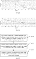
- a power-on voltage output simulation result is shown in FIG. 3 , where label “1" indicates a VCC voltage and label “2" indicates a voltage at the output end Out_put.
- label “1" indicates a VCC voltage
- label "2" indicates a voltage at the output end Out_put.
- the signal at the output end Out_put of the mute control circuit 100 is instantly changed to high voltage level upon power-on and is kept at the high voltage level for a certain period of time, and after that, is changed to be at low voltage level.
- the pop sound is eliminated by the mute circuit 200, thereby improving the mute effect upon power-on.
- the capacitance of the first capacitor C1 and the resistance of the first resistor R1 determines the period of time the high voltage level is maintained. This can be adjusted based on actual needs to satisfy different application scenarios.
- the second capacitor C2 can perform discharging only via the third resistor R3 and the first triode Q1 due to the isolation function of the first diode D1.
- the first capacitor C1 completely releases electric charges immediately via the second diode D2 such that the base electrode of the first triode Q1 is at low voltage level.
- the first triode Q1 Since the emitter electrode of the first triode Q1 is at high voltage level under the discharging of the second capacitor C2, the first triode Q1 is in the turned-on state and the collector electrode of the first triode Q1 is also at high voltage level, such that the second triode Q2 is in the turned-on state and voltages of the emitter electrode, and the collector electrode of the second triode Q2 are equal to each other and are both at high voltage level. That is, the output end Out_put of the mute control circuit 100 outputs high voltage level to the mute circuit 200 to control the mute circuit 200 to be activated.
- the first triode Q1 is in a turned-off state due to voltage decrease of the emitter electrode, and the collector electrode outputs low voltage level to the second triode Q2 such that the second triode Q2 is also in the turned-off state, thereby controlling the output end Out_put to output low voltage level to the mute circuit 200.
- a power-off voltage output simulation result is shown in FIG. 4 , where label “1" indicates a VCC voltage and label “2" indicates a voltage at the output end Out_put.
- label “1" indicates a VCC voltage
- label "2" indicates a voltage at the output end Out_put.
- the signal at the output end Out_put of the mute control circuit 100 is instantly changed to high voltage level upon power-off and is kept at the high voltage level for a certain period of time, and after that, is changed to be at low voltage level.
- the pop sound is eliminated by the mute circuit 200, thereby improving the mute effect upon power-off.
- the capacitance of the second capacitor C2 and the resistance of the first resistor R1 determines the period of time the high voltage level is maintained. This can be adjusted based on actual needs to satisfy different application scenarios.
- the present invention further correspondingly provides a mute control method used upon power-on or power-off.
- the mute control method includes steps of:
- Step S100 upon power-on charging or power-off discharging, utilizing a charge/discharge module to output a first level to a first switch module to control the first switch module to be in a turned-on state;
- Step S200 - utilizing the first switch module to output a second level to a second switch module to control the second switch module to be in the turned-on state;
- Step S300 - utilizing the second switch module to output high voltage level to a mute circuit to control the mute circuit to be activated.
- the present invention further correspondingly provides an audio device including a power supply end, a mute circuit and the afore-described mute control circuit used upon power-on or power-off.
- the mute control circuit used upon power-on or power-off has been described detailedly above, and is not repeated herein.
- the mute control circuit used upon power-on or power-off is connected to a power supply end and a mute circuit of the audio device, the mute control circuit used upon power-on or power-off includes a charge/discharge module, a first switch module and a second switch module; the charge/discharge module is charged from the power supply end upon power-on, the charge/discharge module discharges into the power supply end upon power-off, the charge/discharge module outputs a first level to the first switch module upon charging or discharging to control the first switch module to be in a turned-on state, the first switch module outputs a second level to the second switch module to control the second switch module to be in the turned-on state, the second switch module outputs high voltage level to the mute circuit to control the mute circuit to be activated.
- the high voltage level can be outputted to the mute circuit during power-on and power-off processes to control the mute circuit to be activated, thereby eliminating the pop sound generated upon power-on and power-off and improving user experience on the audio device.
Landscapes
- Engineering & Computer Science (AREA)
- Physics & Mathematics (AREA)
- Acoustics & Sound (AREA)
- Signal Processing (AREA)
- Theoretical Computer Science (AREA)
- General Engineering & Computer Science (AREA)
- General Physics & Mathematics (AREA)
- Amplifiers (AREA)
Applications Claiming Priority (2)
| Application Number | Priority Date | Filing Date | Title |
|---|---|---|---|
| CN201710679849.XA CN107396243A (zh) | 2017-08-10 | 2017-08-10 | 一种开关机静音控制电路、控制方法及音频设备 |
| PCT/CN2018/099372 WO2019029563A1 (zh) | 2017-08-10 | 2018-08-08 | 开关机静音控制电路、控制方法及音频设备 |
Publications (3)
| Publication Number | Publication Date |
|---|---|
| EP3668111A1 true EP3668111A1 (de) | 2020-06-17 |
| EP3668111A4 EP3668111A4 (de) | 2021-04-28 |
| EP3668111B1 EP3668111B1 (de) | 2023-10-04 |
Family
ID=60355402
Family Applications (1)
| Application Number | Title | Priority Date | Filing Date |
|---|---|---|---|
| EP18844308.9A Active EP3668111B1 (de) | 2017-08-10 | 2018-08-08 | Beim umschalten oder ausschalten verwendete stummsteuerverfahren und audiovorrichtung |
Country Status (4)
| Country | Link |
|---|---|
| US (1) | US10826455B2 (de) |
| EP (1) | EP3668111B1 (de) |
| CN (1) | CN107396243A (de) |
| WO (1) | WO2019029563A1 (de) |
Families Citing this family (13)
| Publication number | Priority date | Publication date | Assignee | Title |
|---|---|---|---|---|
| CN107396243A (zh) * | 2017-08-10 | 2017-11-24 | 惠州Tcl移动通信有限公司 | 一种开关机静音控制电路、控制方法及音频设备 |
| CN110290446B (zh) * | 2019-06-11 | 2021-09-07 | 晶晨半导体(上海)股份有限公司 | 一种快速开关机防止爆音的静音电路 |
| CN110662136A (zh) * | 2019-09-23 | 2020-01-07 | 深圳市华星光电技术有限公司 | 音频装置及显示面板 |
| CN110602605B (zh) * | 2019-10-11 | 2024-05-14 | 广东美的白色家电技术创新中心有限公司 | 语音开关电路和语音设备 |
| CN111263268B (zh) * | 2020-01-15 | 2022-02-01 | 深圳创维数字技术有限公司 | 一种断电时喇叭pop音消除电路及电子产品 |
| CN114697828B (zh) * | 2020-12-31 | 2024-11-01 | 广州艾美网络科技有限公司 | 功放控制电路、电源控制电路及音频设备 |
| CN112954546A (zh) * | 2021-02-01 | 2021-06-11 | 广州朗国电子科技有限公司 | 一种上电下电去爆破音的控制电路、模块及终端设备 |
| CN113098462B (zh) * | 2021-04-02 | 2023-12-22 | 上海季丰电子股份有限公司 | 一种快速上下电电路及其控制方法 |
| CN113115180B (zh) * | 2021-04-28 | 2022-08-02 | 广州朗国电子科技股份有限公司 | 一种音频输出端的爆破音去除装置及音频设备 |
| CN113676819B (zh) * | 2021-10-21 | 2022-01-07 | 武汉市聚芯微电子有限责任公司 | 软静音控制电路、软静音控制方法以及设备 |
| CN114125660B (zh) * | 2021-11-23 | 2023-08-15 | 深圳市长丰影像器材有限公司 | 一种消除开机爆破音的音频系统及供电控制方法 |
| CN115103272B (zh) * | 2022-08-24 | 2022-12-02 | 上海芯龙半导体技术股份有限公司南京分公司 | 静音控制方法、音频功放电路以及音频功放芯片 |
| CN115767370A (zh) * | 2022-09-21 | 2023-03-07 | 广东南控云图科技有限公司 | 一种消除开机噪音的音频控制电路及音频设备 |
Family Cites Families (21)
| Publication number | Priority date | Publication date | Assignee | Title |
|---|---|---|---|---|
| KR200151266Y1 (ko) * | 1996-11-27 | 1999-07-15 | 윤종용 | 오디오시스템에서 전원 온/오 프시 잡음 제거 회로 |
| TWI230557B (en) * | 2003-11-06 | 2005-04-01 | Liteon It Corp | Mute circuit for use in the duration of power switching |
| TW200726293A (en) * | 2005-12-29 | 2007-07-01 | Tatung Co | Muting circuit capable of eliminating noise generated in powering off and electronic apparatus incorporating the muting circuit |
| CN200953603Y (zh) * | 2006-10-18 | 2007-09-26 | 青岛海信电器股份有限公司 | 开关机静音电路及具有所述静音电路的电视机 |
| CN100546186C (zh) * | 2006-10-30 | 2009-09-30 | 青岛海信电器股份有限公司 | 开关机静音电路 |
| US8218793B2 (en) * | 2006-12-11 | 2012-07-10 | Mediatek Inc. | Apparatus and muting circuit |
| JP2009218822A (ja) * | 2008-03-10 | 2009-09-24 | Toshiba Corp | ミュート回路 |
| CN201238284Y (zh) * | 2008-08-01 | 2009-05-13 | 青岛海信宽带多媒体技术股份有限公司 | 开关机静音电路及具有所述静音电路的机顶盒 |
| US20100183166A1 (en) * | 2009-01-20 | 2010-07-22 | Simon Shan Lin Sun | External car amplifier capable of producing high power |
| TW201107952A (en) * | 2009-08-25 | 2011-03-01 | Elitegroup Computer Systems Co Ltd | Power-supply expansion system and its method thereof |
| TWI410144B (zh) * | 2010-01-11 | 2013-09-21 | Hon Hai Prec Ind Co Ltd | 爆音抑制電路 |
| CN102333264A (zh) * | 2010-07-15 | 2012-01-25 | 鸿富锦精密工业(深圳)有限公司 | 静音控制电路及具有该静音控制电路的电子装置 |
| CN202059555U (zh) * | 2010-12-23 | 2011-11-30 | 康佳集团股份有限公司 | 一种消除开机杂音的电路 |
| CN203104756U (zh) * | 2013-02-21 | 2013-07-31 | 深圳市中通福瑞电子科技有限公司 | 一种开关机静音电路 |
| JP2014191253A (ja) * | 2013-03-28 | 2014-10-06 | Panasonic Corp | オーディオ再生装置 |
| EP2879270B1 (de) * | 2013-04-17 | 2016-09-21 | Huawei Technologies Co., Ltd. | Identifikationsschaltung einer stromversorgung und stromgetriebene vorrichtung |
| CN203708454U (zh) * | 2013-09-11 | 2014-07-09 | 东莞市远峰科技有限公司 | 一种用于消除电视盒的音频噪声电路 |
| CN205666814U (zh) * | 2016-06-13 | 2016-10-26 | 浪潮集团有限公司 | 一种用于消除Speaker Pop声的电路 |
| JP6315125B2 (ja) * | 2017-03-23 | 2018-04-25 | ヤマハ株式会社 | 信号処理装置およびプログラム |
| CN206865726U (zh) * | 2017-06-12 | 2018-01-09 | 广州视源电子科技股份有限公司 | 防爆音电路及电子设备 |
| CN107396243A (zh) * | 2017-08-10 | 2017-11-24 | 惠州Tcl移动通信有限公司 | 一种开关机静音控制电路、控制方法及音频设备 |
-
2017
- 2017-08-10 CN CN201710679849.XA patent/CN107396243A/zh active Pending
-
2018
- 2018-08-08 EP EP18844308.9A patent/EP3668111B1/de active Active
- 2018-08-08 WO PCT/CN2018/099372 patent/WO2019029563A1/zh not_active Ceased
- 2018-08-08 US US16/637,762 patent/US10826455B2/en active Active
Also Published As
| Publication number | Publication date |
|---|---|
| US20200244241A1 (en) | 2020-07-30 |
| EP3668111A4 (de) | 2021-04-28 |
| US10826455B2 (en) | 2020-11-03 |
| EP3668111B1 (de) | 2023-10-04 |
| WO2019029563A1 (zh) | 2019-02-14 |
| CN107396243A (zh) | 2017-11-24 |
Similar Documents
| Publication | Publication Date | Title |
|---|---|---|
| EP3668111B1 (de) | Beim umschalten oder ausschalten verwendete stummsteuerverfahren und audiovorrichtung | |
| US8199930B2 (en) | Pop noise suppression apparatus and audio output system utilizing the same | |
| JP2013187900A (ja) | イヤホンジャックの駆動回路 | |
| US7917779B2 (en) | Power control apparatus for motherboard | |
| CN103366815A (zh) | 断电保护电路及具有该断电保护电路的电子装置 | |
| CN114697828B (zh) | 功放控制电路、电源控制电路及音频设备 | |
| KR20160070004A (ko) | 전압 검출 회로 | |
| CN108683979B (zh) | 静音电路及音频设备 | |
| EP3065029B1 (de) | Tastempfindungsdarstellungsvorrichtung und verfahren zur steuerung der tastempfindungsdarstellungsvorrichtung | |
| CN110806792A (zh) | 一种硬件开关机电路及电子设备 | |
| CN105262326B (zh) | 一种开关电源输出电压线性启动控制电路 | |
| CN204810138U (zh) | 终端设备的自动开机电路及终端设备 | |
| JP2012226756A (ja) | 電源アダプタ回路 | |
| CN210295865U (zh) | 驱屏供电电路 | |
| CN103683881A (zh) | 加快电源下电速度的电路 | |
| US9298235B2 (en) | Electronic device and power control module | |
| US20140348343A1 (en) | Audio device for suppressing noise | |
| CN101516050B (zh) | 爆音消除装置及使用所述装置的声音输出系统 | |
| US20140139043A1 (en) | Power Off Delay Circuit and Method, and Audio System with Power Off Delay | |
| US20130266153A1 (en) | Anti-pop circuit | |
| CN107817699B (zh) | 控制电路、控制方法和电子设备 | |
| US9130516B2 (en) | POP noise suppression circuit and system | |
| CN217240917U (zh) | Pop音处理电路和播放装置 | |
| CN102098011B (zh) | 音频功率放大器静音快速控制电路 | |
| JP6083429B2 (ja) | ミュート制御回路 |
Legal Events
| Date | Code | Title | Description |
|---|---|---|---|
| STAA | Information on the status of an ep patent application or granted ep patent |
Free format text: STATUS: THE INTERNATIONAL PUBLICATION HAS BEEN MADE |
|
| PUAI | Public reference made under article 153(3) epc to a published international application that has entered the european phase |
Free format text: ORIGINAL CODE: 0009012 |
|
| STAA | Information on the status of an ep patent application or granted ep patent |
Free format text: STATUS: REQUEST FOR EXAMINATION WAS MADE |
|
| 17P | Request for examination filed |
Effective date: 20200211 |
|
| AK | Designated contracting states |
Kind code of ref document: A1 Designated state(s): AL AT BE BG CH CY CZ DE DK EE ES FI FR GB GR HR HU IE IS IT LI LT LU LV MC MK MT NL NO PL PT RO RS SE SI SK SM TR |
|
| AX | Request for extension of the european patent |
Extension state: BA ME |
|
| DAV | Request for validation of the european patent (deleted) | ||
| DAX | Request for extension of the european patent (deleted) | ||
| A4 | Supplementary search report drawn up and despatched |
Effective date: 20210329 |
|
| RIC1 | Information provided on ipc code assigned before grant |
Ipc: H04R 3/00 20060101AFI20210323BHEP |
|
| REG | Reference to a national code |
Ref country code: DE Free format text: PREVIOUS MAIN CLASS: H04R0003000000 Ipc: H03G0003340000 Ref country code: DE Ref legal event code: R079 Ref document number: 602018058829 Country of ref document: DE Free format text: PREVIOUS MAIN CLASS: H04R0003000000 Ipc: H03G0003340000 |
|
| GRAP | Despatch of communication of intention to grant a patent |
Free format text: ORIGINAL CODE: EPIDOSNIGR1 |
|
| STAA | Information on the status of an ep patent application or granted ep patent |
Free format text: STATUS: GRANT OF PATENT IS INTENDED |
|
| RIC1 | Information provided on ipc code assigned before grant |
Ipc: H03G 3/34 20060101AFI20230428BHEP |
|
| INTG | Intention to grant announced |
Effective date: 20230525 |
|
| P01 | Opt-out of the competence of the unified patent court (upc) registered |
Effective date: 20230622 |
|
| GRAS | Grant fee paid |
Free format text: ORIGINAL CODE: EPIDOSNIGR3 |
|
| GRAA | (expected) grant |
Free format text: ORIGINAL CODE: 0009210 |
|
| STAA | Information on the status of an ep patent application or granted ep patent |
Free format text: STATUS: THE PATENT HAS BEEN GRANTED |
|
| AK | Designated contracting states |
Kind code of ref document: B1 Designated state(s): AL AT BE BG CH CY CZ DE DK EE ES FI FR GB GR HR HU IE IS IT LI LT LU LV MC MK MT NL NO PL PT RO RS SE SI SK SM TR |
|
| REG | Reference to a national code |
Ref country code: GB Ref legal event code: FG4D |
|
| REG | Reference to a national code |
Ref country code: CH Ref legal event code: EP |
|
| REG | Reference to a national code |
Ref country code: IE Ref legal event code: FG4D |
|
| REG | Reference to a national code |
Ref country code: DE Ref legal event code: R096 Ref document number: 602018058829 Country of ref document: DE |
|
| REG | Reference to a national code |
Ref country code: LT Ref legal event code: MG9D |
|
| REG | Reference to a national code |
Ref country code: NL Ref legal event code: MP Effective date: 20231004 |
|
| REG | Reference to a national code |
Ref country code: AT Ref legal event code: MK05 Ref document number: 1618806 Country of ref document: AT Kind code of ref document: T Effective date: 20231004 |
|
| PG25 | Lapsed in a contracting state [announced via postgrant information from national office to epo] |
Ref country code: NL Free format text: LAPSE BECAUSE OF FAILURE TO SUBMIT A TRANSLATION OF THE DESCRIPTION OR TO PAY THE FEE WITHIN THE PRESCRIBED TIME-LIMIT Effective date: 20231004 |
|
| PG25 | Lapsed in a contracting state [announced via postgrant information from national office to epo] |
Ref country code: GR Free format text: LAPSE BECAUSE OF FAILURE TO SUBMIT A TRANSLATION OF THE DESCRIPTION OR TO PAY THE FEE WITHIN THE PRESCRIBED TIME-LIMIT Effective date: 20240105 |
|
| PG25 | Lapsed in a contracting state [announced via postgrant information from national office to epo] |
Ref country code: IS Free format text: LAPSE BECAUSE OF FAILURE TO SUBMIT A TRANSLATION OF THE DESCRIPTION OR TO PAY THE FEE WITHIN THE PRESCRIBED TIME-LIMIT Effective date: 20240204 |
|
| PG25 | Lapsed in a contracting state [announced via postgrant information from national office to epo] |
Ref country code: LT Free format text: LAPSE BECAUSE OF FAILURE TO SUBMIT A TRANSLATION OF THE DESCRIPTION OR TO PAY THE FEE WITHIN THE PRESCRIBED TIME-LIMIT Effective date: 20231004 |
|
| PG25 | Lapsed in a contracting state [announced via postgrant information from national office to epo] |
Ref country code: AT Free format text: LAPSE BECAUSE OF FAILURE TO SUBMIT A TRANSLATION OF THE DESCRIPTION OR TO PAY THE FEE WITHIN THE PRESCRIBED TIME-LIMIT Effective date: 20231004 |
|
| PG25 | Lapsed in a contracting state [announced via postgrant information from national office to epo] |
Ref country code: ES Free format text: LAPSE BECAUSE OF FAILURE TO SUBMIT A TRANSLATION OF THE DESCRIPTION OR TO PAY THE FEE WITHIN THE PRESCRIBED TIME-LIMIT Effective date: 20231004 |
|
| PG25 | Lapsed in a contracting state [announced via postgrant information from national office to epo] |
Ref country code: LT Free format text: LAPSE BECAUSE OF FAILURE TO SUBMIT A TRANSLATION OF THE DESCRIPTION OR TO PAY THE FEE WITHIN THE PRESCRIBED TIME-LIMIT Effective date: 20231004 Ref country code: IS Free format text: LAPSE BECAUSE OF FAILURE TO SUBMIT A TRANSLATION OF THE DESCRIPTION OR TO PAY THE FEE WITHIN THE PRESCRIBED TIME-LIMIT Effective date: 20240204 Ref country code: GR Free format text: LAPSE BECAUSE OF FAILURE TO SUBMIT A TRANSLATION OF THE DESCRIPTION OR TO PAY THE FEE WITHIN THE PRESCRIBED TIME-LIMIT Effective date: 20240105 Ref country code: ES Free format text: LAPSE BECAUSE OF FAILURE TO SUBMIT A TRANSLATION OF THE DESCRIPTION OR TO PAY THE FEE WITHIN THE PRESCRIBED TIME-LIMIT Effective date: 20231004 Ref country code: BG Free format text: LAPSE BECAUSE OF FAILURE TO SUBMIT A TRANSLATION OF THE DESCRIPTION OR TO PAY THE FEE WITHIN THE PRESCRIBED TIME-LIMIT Effective date: 20240104 Ref country code: AT Free format text: LAPSE BECAUSE OF FAILURE TO SUBMIT A TRANSLATION OF THE DESCRIPTION OR TO PAY THE FEE WITHIN THE PRESCRIBED TIME-LIMIT Effective date: 20231004 Ref country code: PT Free format text: LAPSE BECAUSE OF FAILURE TO SUBMIT A TRANSLATION OF THE DESCRIPTION OR TO PAY THE FEE WITHIN THE PRESCRIBED TIME-LIMIT Effective date: 20240205 |
|
| PG25 | Lapsed in a contracting state [announced via postgrant information from national office to epo] |
Ref country code: SE Free format text: LAPSE BECAUSE OF FAILURE TO SUBMIT A TRANSLATION OF THE DESCRIPTION OR TO PAY THE FEE WITHIN THE PRESCRIBED TIME-LIMIT Effective date: 20231004 Ref country code: RS Free format text: LAPSE BECAUSE OF FAILURE TO SUBMIT A TRANSLATION OF THE DESCRIPTION OR TO PAY THE FEE WITHIN THE PRESCRIBED TIME-LIMIT Effective date: 20231004 Ref country code: PL Free format text: LAPSE BECAUSE OF FAILURE TO SUBMIT A TRANSLATION OF THE DESCRIPTION OR TO PAY THE FEE WITHIN THE PRESCRIBED TIME-LIMIT Effective date: 20231004 Ref country code: NO Free format text: LAPSE BECAUSE OF FAILURE TO SUBMIT A TRANSLATION OF THE DESCRIPTION OR TO PAY THE FEE WITHIN THE PRESCRIBED TIME-LIMIT Effective date: 20240104 Ref country code: LV Free format text: LAPSE BECAUSE OF FAILURE TO SUBMIT A TRANSLATION OF THE DESCRIPTION OR TO PAY THE FEE WITHIN THE PRESCRIBED TIME-LIMIT Effective date: 20231004 Ref country code: HR Free format text: LAPSE BECAUSE OF FAILURE TO SUBMIT A TRANSLATION OF THE DESCRIPTION OR TO PAY THE FEE WITHIN THE PRESCRIBED TIME-LIMIT Effective date: 20231004 |
|
| REG | Reference to a national code |
Ref country code: DE Ref legal event code: R097 Ref document number: 602018058829 Country of ref document: DE |
|
| PG25 | Lapsed in a contracting state [announced via postgrant information from national office to epo] |
Ref country code: DK Free format text: LAPSE BECAUSE OF FAILURE TO SUBMIT A TRANSLATION OF THE DESCRIPTION OR TO PAY THE FEE WITHIN THE PRESCRIBED TIME-LIMIT Effective date: 20231004 |
|
| PG25 | Lapsed in a contracting state [announced via postgrant information from national office to epo] |
Ref country code: CZ Free format text: LAPSE BECAUSE OF FAILURE TO SUBMIT A TRANSLATION OF THE DESCRIPTION OR TO PAY THE FEE WITHIN THE PRESCRIBED TIME-LIMIT Effective date: 20231004 |
|
| PG25 | Lapsed in a contracting state [announced via postgrant information from national office to epo] |
Ref country code: SK Free format text: LAPSE BECAUSE OF FAILURE TO SUBMIT A TRANSLATION OF THE DESCRIPTION OR TO PAY THE FEE WITHIN THE PRESCRIBED TIME-LIMIT Effective date: 20231004 |
|
| PG25 | Lapsed in a contracting state [announced via postgrant information from national office to epo] |
Ref country code: SM Free format text: LAPSE BECAUSE OF FAILURE TO SUBMIT A TRANSLATION OF THE DESCRIPTION OR TO PAY THE FEE WITHIN THE PRESCRIBED TIME-LIMIT Effective date: 20231004 Ref country code: SK Free format text: LAPSE BECAUSE OF FAILURE TO SUBMIT A TRANSLATION OF THE DESCRIPTION OR TO PAY THE FEE WITHIN THE PRESCRIBED TIME-LIMIT Effective date: 20231004 Ref country code: RO Free format text: LAPSE BECAUSE OF FAILURE TO SUBMIT A TRANSLATION OF THE DESCRIPTION OR TO PAY THE FEE WITHIN THE PRESCRIBED TIME-LIMIT Effective date: 20231004 Ref country code: IT Free format text: LAPSE BECAUSE OF FAILURE TO SUBMIT A TRANSLATION OF THE DESCRIPTION OR TO PAY THE FEE WITHIN THE PRESCRIBED TIME-LIMIT Effective date: 20231004 Ref country code: EE Free format text: LAPSE BECAUSE OF FAILURE TO SUBMIT A TRANSLATION OF THE DESCRIPTION OR TO PAY THE FEE WITHIN THE PRESCRIBED TIME-LIMIT Effective date: 20231004 Ref country code: DK Free format text: LAPSE BECAUSE OF FAILURE TO SUBMIT A TRANSLATION OF THE DESCRIPTION OR TO PAY THE FEE WITHIN THE PRESCRIBED TIME-LIMIT Effective date: 20231004 Ref country code: CZ Free format text: LAPSE BECAUSE OF FAILURE TO SUBMIT A TRANSLATION OF THE DESCRIPTION OR TO PAY THE FEE WITHIN THE PRESCRIBED TIME-LIMIT Effective date: 20231004 |
|
| PLBE | No opposition filed within time limit |
Free format text: ORIGINAL CODE: 0009261 |
|
| STAA | Information on the status of an ep patent application or granted ep patent |
Free format text: STATUS: NO OPPOSITION FILED WITHIN TIME LIMIT |
|
| 26N | No opposition filed |
Effective date: 20240705 |
|
| PG25 | Lapsed in a contracting state [announced via postgrant information from national office to epo] |
Ref country code: SI Free format text: LAPSE BECAUSE OF FAILURE TO SUBMIT A TRANSLATION OF THE DESCRIPTION OR TO PAY THE FEE WITHIN THE PRESCRIBED TIME-LIMIT Effective date: 20231004 |
|
| PG25 | Lapsed in a contracting state [announced via postgrant information from national office to epo] |
Ref country code: SI Free format text: LAPSE BECAUSE OF FAILURE TO SUBMIT A TRANSLATION OF THE DESCRIPTION OR TO PAY THE FEE WITHIN THE PRESCRIBED TIME-LIMIT Effective date: 20231004 |
|
| REG | Reference to a national code |
Ref country code: CH Ref legal event code: PL |
|
| PG25 | Lapsed in a contracting state [announced via postgrant information from national office to epo] |
Ref country code: LU Free format text: LAPSE BECAUSE OF NON-PAYMENT OF DUE FEES Effective date: 20240808 |
|
| PG25 | Lapsed in a contracting state [announced via postgrant information from national office to epo] |
Ref country code: CH Free format text: LAPSE BECAUSE OF NON-PAYMENT OF DUE FEES Effective date: 20240831 Ref country code: MC Free format text: LAPSE BECAUSE OF FAILURE TO SUBMIT A TRANSLATION OF THE DESCRIPTION OR TO PAY THE FEE WITHIN THE PRESCRIBED TIME-LIMIT Effective date: 20231004 |
|
| REG | Reference to a national code |
Ref country code: BE Ref legal event code: MM Effective date: 20240831 |
|
| PG25 | Lapsed in a contracting state [announced via postgrant information from national office to epo] |
Ref country code: BE Free format text: LAPSE BECAUSE OF NON-PAYMENT OF DUE FEES Effective date: 20240831 |
|
| PG25 | Lapsed in a contracting state [announced via postgrant information from national office to epo] |
Ref country code: IE Free format text: LAPSE BECAUSE OF NON-PAYMENT OF DUE FEES Effective date: 20240808 |
|
| PG25 | Lapsed in a contracting state [announced via postgrant information from national office to epo] |
Ref country code: FI Free format text: LAPSE BECAUSE OF FAILURE TO SUBMIT A TRANSLATION OF THE DESCRIPTION OR TO PAY THE FEE WITHIN THE PRESCRIBED TIME-LIMIT Effective date: 20231004 |
|
| PGFP | Annual fee paid to national office [announced via postgrant information from national office to epo] |
Ref country code: DE Payment date: 20250820 Year of fee payment: 8 |
|
| PGFP | Annual fee paid to national office [announced via postgrant information from national office to epo] |
Ref country code: GB Payment date: 20250820 Year of fee payment: 8 |
|
| PGFP | Annual fee paid to national office [announced via postgrant information from national office to epo] |
Ref country code: FR Payment date: 20250828 Year of fee payment: 8 |
|
| PG25 | Lapsed in a contracting state [announced via postgrant information from national office to epo] |
Ref country code: CY Free format text: LAPSE BECAUSE OF FAILURE TO SUBMIT A TRANSLATION OF THE DESCRIPTION OR TO PAY THE FEE WITHIN THE PRESCRIBED TIME-LIMIT; INVALID AB INITIO Effective date: 20180808 |
|
| PG25 | Lapsed in a contracting state [announced via postgrant information from national office to epo] |
Ref country code: HU Free format text: LAPSE BECAUSE OF FAILURE TO SUBMIT A TRANSLATION OF THE DESCRIPTION OR TO PAY THE FEE WITHIN THE PRESCRIBED TIME-LIMIT; INVALID AB INITIO Effective date: 20180808 |