EP3671247A1 - Verfahren zur bewertung der elektrischen eigenschaften eines hts-supraleiters - Google Patents
Verfahren zur bewertung der elektrischen eigenschaften eines hts-supraleiters Download PDFInfo
- Publication number
- EP3671247A1 EP3671247A1 EP18213831.3A EP18213831A EP3671247A1 EP 3671247 A1 EP3671247 A1 EP 3671247A1 EP 18213831 A EP18213831 A EP 18213831A EP 3671247 A1 EP3671247 A1 EP 3671247A1
- Authority
- EP
- European Patent Office
- Prior art keywords
- hts superconductor
- current
- magnetic field
- hts
- superconductor
- Prior art date
- Legal status (The legal status is an assumption and is not a legal conclusion. Google has not performed a legal analysis and makes no representation as to the accuracy of the status listed.)
- Withdrawn
Links
- 239000002887 superconductor Substances 0.000 title claims abstract description 225
- 238000000034 method Methods 0.000 title claims abstract description 52
- 230000005291 magnetic effect Effects 0.000 claims abstract description 161
- 238000005259 measurement Methods 0.000 claims abstract description 73
- 238000012512 characterization method Methods 0.000 claims abstract description 70
- 238000011156 evaluation Methods 0.000 claims abstract description 17
- 230000004907 flux Effects 0.000 claims description 36
- 230000007547 defect Effects 0.000 claims description 24
- 230000002093 peripheral effect Effects 0.000 claims description 21
- 238000013519 translation Methods 0.000 claims description 13
- 238000010438 heat treatment Methods 0.000 claims description 10
- 238000012216 screening Methods 0.000 claims description 10
- 238000003776 cleavage reaction Methods 0.000 claims description 8
- 230000005294 ferromagnetic effect Effects 0.000 claims description 8
- 230000007017 scission Effects 0.000 claims description 8
- 238000012544 monitoring process Methods 0.000 claims description 7
- 230000001105 regulatory effect Effects 0.000 claims description 4
- 239000004020 conductor Substances 0.000 abstract description 15
- 238000012360 testing method Methods 0.000 abstract description 11
- 238000002347 injection Methods 0.000 abstract description 6
- 239000007924 injection Substances 0.000 abstract description 6
- 238000011161 development Methods 0.000 description 7
- 230000018109 developmental process Effects 0.000 description 7
- 230000000694 effects Effects 0.000 description 7
- 239000000463 material Substances 0.000 description 6
- 238000001816 cooling Methods 0.000 description 5
- 238000013461 design Methods 0.000 description 5
- 238000010586 diagram Methods 0.000 description 5
- 230000012447 hatching Effects 0.000 description 4
- 230000001965 increasing effect Effects 0.000 description 4
- 239000000758 substrate Substances 0.000 description 4
- 238000004804 winding Methods 0.000 description 4
- 238000004458 analytical method Methods 0.000 description 3
- 229910052751 metal Inorganic materials 0.000 description 3
- 239000002184 metal Substances 0.000 description 3
- 230000009467 reduction Effects 0.000 description 3
- IJGRMHOSHXDMSA-UHFFFAOYSA-N Atomic nitrogen Chemical compound N#N IJGRMHOSHXDMSA-UHFFFAOYSA-N 0.000 description 2
- RYGMFSIKBFXOCR-UHFFFAOYSA-N Copper Chemical compound [Cu] RYGMFSIKBFXOCR-UHFFFAOYSA-N 0.000 description 2
- 238000013459 approach Methods 0.000 description 2
- 229910052802 copper Inorganic materials 0.000 description 2
- 239000010949 copper Substances 0.000 description 2
- 238000005314 correlation function Methods 0.000 description 2
- 238000001514 detection method Methods 0.000 description 2
- 230000036962 time dependent Effects 0.000 description 2
- 230000001052 transient effect Effects 0.000 description 2
- 208000032365 Electromagnetic interference Diseases 0.000 description 1
- 230000000903 blocking effect Effects 0.000 description 1
- 238000004364 calculation method Methods 0.000 description 1
- 239000000919 ceramic Substances 0.000 description 1
- 238000010168 coupling process Methods 0.000 description 1
- 238000005859 coupling reaction Methods 0.000 description 1
- 230000002950 deficient Effects 0.000 description 1
- 230000001419 dependent effect Effects 0.000 description 1
- 238000005516 engineering process Methods 0.000 description 1
- 230000001747 exhibiting effect Effects 0.000 description 1
- 239000003302 ferromagnetic material Substances 0.000 description 1
- 239000007789 gas Substances 0.000 description 1
- 230000001939 inductive effect Effects 0.000 description 1
- 230000010354 integration Effects 0.000 description 1
- 238000011835 investigation Methods 0.000 description 1
- 239000007788 liquid Substances 0.000 description 1
- 239000000203 mixture Substances 0.000 description 1
- 229910052757 nitrogen Inorganic materials 0.000 description 1
- 235000012771 pancakes Nutrition 0.000 description 1
- 229910052761 rare earth metal Inorganic materials 0.000 description 1
- 230000004044 response Effects 0.000 description 1
- 238000007493 shaping process Methods 0.000 description 1
- 229910001220 stainless steel Inorganic materials 0.000 description 1
- 239000010935 stainless steel Substances 0.000 description 1
- 239000000126 substance Substances 0.000 description 1
- 230000001629 suppression Effects 0.000 description 1
- 238000010408 sweeping Methods 0.000 description 1
- 238000012546 transfer Methods 0.000 description 1
- 230000007704 transition Effects 0.000 description 1
Images





Classifications
-
- G—PHYSICS
- G01—MEASURING; TESTING
- G01R—MEASURING ELECTRIC VARIABLES; MEASURING MAGNETIC VARIABLES
- G01R33/00—Arrangements or instruments for measuring magnetic variables
- G01R33/12—Measuring magnetic properties of articles or specimens of solids or fluids
- G01R33/1238—Measuring superconductive properties
-
- G—PHYSICS
- G01—MEASURING; TESTING
- G01R—MEASURING ELECTRIC VARIABLES; MEASURING MAGNETIC VARIABLES
- G01R33/00—Arrangements or instruments for measuring magnetic variables
- G01R33/12—Measuring magnetic properties of articles or specimens of solids or fluids
- G01R33/1238—Measuring superconductive properties
- G01R33/1246—Measuring critical current
-
- G—PHYSICS
- G01—MEASURING; TESTING
- G01R—MEASURING ELECTRIC VARIABLES; MEASURING MAGNETIC VARIABLES
- G01R33/00—Arrangements or instruments for measuring magnetic variables
- G01R33/12—Measuring magnetic properties of articles or specimens of solids or fluids
- G01R33/1215—Measuring magnetisation; Particular magnetometers therefor
Definitions
- the invention relates to a method for evaluating the electrical properties of a HTS superconductor, in particular a HTS superconductor tape, wherein the HTS superconductor is exposed to a cryogenic environment of a temperature T env , wherein the HTS superconductor passes through a characterization zone where a magnetic field is applied to the HTS superconductor, wherein the characterization zone comprises a central region and two peripheral regions through which the HTS superconductor passes, and wherein the HTS superconductor is supplied with a measuring current by two current exchange elements, wherein one of the current exchange elements contacts the HTS superconductor in each peripheral region.
- Superconductors can be used to carry an electric current at practically no ohmic losses, for example in order to produce high strength magnetic fields in superconducting magnet coils, or simply to transport the current from a source to a consumer.
- Superconductor materials have to be cooled down to a critical temperature T crit specific to the superconductor material to become superconducting; cooling a superconductor further below its critical temperature T crit increases the strength of an electrical current (or electrical current density) the superconductor may carry and the strength of a magnetic field the superconductor material may be exposed to while staying superconducting.
- an important electric characteristic of a particular superconductor is the maximum electrical current strength that a superconductor may carry at a given temperature (or operating temperature) and a given magnetic field strength (or operating magnetic field strength). This maximum electrical current strength is called the critical current I crit .
- High temperature superconductors require less cooling as compared to conventional low temperature superconductors (LTS), i.e. HTS superconductors have a higher T crit as compared to LTS superconductors; often HTS materials have a T crit of 77 K or higher.
- HTS superconductors when operating HTS superconductors at temperatures far below their critical temperature T crit , they may carry much higher electric currents as compared to LTS superconductors.
- producing HTS superconductors is rather difficult as compared to conventional metallic LTS superconductors, in particular since HTS materials are typically ceramic and require a rather specific chemical composition and microstructure.
- Commercial HTS superconductors are typically of tape type (also known as coated conductors), wherein a superconductor layer is deposited on a flexible substrate, such as a metal substrate, typically applying one or more buffer layers in between.
- HTS superconductors in general include occasional defects that limit the current carrying capacity. Accordingly, the quality of a manufactured HTS should be checked by evaluating their electrical characteristics before using them in practical applications.
- L. Rossi et al. have suggested to measure the critical current of a ReBCO type coated conductor every 2 cm.
- the coated conductor is wound from a first reel to a second reel, passing over roller type current contacts. Between the roller type current contacts, the coated conductor passes voltage taps with an electromagnet in between, and voltage taps with a rotating permanent magnet in between.
- the whole coated conductor including the reels, the current contacts, the voltage taps and the magnets are located in a LN2 bath; the applied magnetic field was about 0.5 Tesla. Further, it is suggested to predict 4.2 K, high field tape properties from the in-field measurements at 77 K.
- the setup my give indications of quality variations of a coated conductor
- the electrical characterization has been found to be susceptible to measurement errors. In particular, it is difficult to distinguish defects in the material from measurement errors. So making reliable predictions on the behaviour of the coated conductor in practice is difficult to obtain.
- US 2007/0149411 A1 proposes to measure electrical characteristics of a superconducting tape at a plurality of positions along its length.
- the tape is wound between two reels, wherein the tape is guided by guiding rolls through a characterization zone where a pair of permanent magnets may be rotated about the tape.
- Both non-contact and direct contact testing methods for the tape are proposed, however no details are given where to set up contact elements.
- the HTS superconductor is continuously translated from a first reservoir through the characterization zone to a second reservoir, that the HTS superconductor is exposed to the cryogenic environment only in a cryogenic zone, wherein the cryogenic zone includes the characterization zone and wherein the first and second reservoir are located outside the cryogenic zone, that the HTS superconductor passes two buffer zones where two de-coupling sections are created in the HTS superconductor, with a first decoupling section established between the first reservoir and the characterization zone, and a second decoupling section established between the characterization zone and the second reservoir, that the magnetic field is chosen such that a maximum magnetic flux density at the HTS superconductor in the central region is B centr , with B centr ⁇ 1.5 Tesla, and a maximum magnetic flux density at the HTS superconductor at the current exchange elements is B peri , such that, at the temperature T env of the HTS superconductor established by
- the inventive method suggest a plurality of measures to be applied in order to achieve a more reliable electric characterization of the HTS superconductor.
- the cryogenic environment is only applied in a cryogenic zone, which in particular does not include the first and second reservoir of the HTS superconductor. This makes the setup simpler, and intrinsically minimizes possible disturbance impact from most of the HTS superconductor.
- the method suggests to put the current exchange elements (current contacts) in a respective peripheral region where the local critical current is significantly higher than in the characterization zone, typically by having a much lower absolute value of magnetic flux density (or magnetic field strength) there; this avoids measurement errors by a varying electrical contact quality.
- the invention suggests buffer zones in the setup, and corresponding decoupling sections in the HTS superconductor. These help in blocking leakage currents and antenna-effect currents, and thus avoid corresponding measurement errors.
- the measures allow a continuous HTS superconductor translation and measurement, which is fast and thorough.
- the method establishes one or a plurality of electric characteristics of the HTS superconductor, indicating a superconducting performance of the HTS conductor.
- a transition between superconducting state and normally conducting state is monitored or checked for, such as by measuring a critical current or a critical magnetic field as a function of the position along the HTS superconductor.
- a relatively high magnetic flux density B centr is used at the HTS superconductor at the central region, namely with B centr ⁇ 1.5 Tesla, which has been found to allow a more accurate estimation of the behaviour of the HTS superconductor at higher fields such as at B high ⁇ 10 Tesla and at lower temperatures such as T low ⁇ 4.2 K.
- B centr ⁇ 1.5 Tesla has been found to allow a more accurate estimation of the behaviour of the HTS superconductor at higher fields such as at B high ⁇ 10 Tesla and at lower temperatures such as T low ⁇ 4.2 K.
- the HTS superconductor is typically kept significantly above 4.2K, such as 30 K or above, in particular to save cooling costs.
- the maximum magnetic flux density of B centr is present only at a relatively short section of the HTS superconductor tape in the central region ("magnetic knife"), such as of only 20 mm in length or less, or even 5 mm in length or less, and the information about the HTS superconductor quality is basically obtained from this section.
- magnetic knife such as of only 20 mm in length or less, or even 5 mm in length or less
- other parts of the HTS superconductor between the current exchange elements or between voltage pick-up elements may still contribute to the measurement result.
- the "active" electrical contact area of the current exchange elements with the HTS superconductor may vary during superconductor translation significantly.
- the variation of "active" contact area may bring the HTS superconductor to the limits of its (local) current carrying capacity, what may influence the measurement current actually transferred into the HTS superconductor (in particular reduce it at times of bad contact) and a related measurement voltage.
- the invention proposes to locate the current exchange contacts such that the electrical exchange elements are placed at the periphery of the generated magnetic field, where (due to a lower magnetic flux density) the critical current (or the critical current density, respectively) is significantly higher than in the central region. Then a varying "active" electrical contact area at the current exchange elements, which leads to a varying current density locally near the current exchange elements, is less likely to come close to the limits of the current carrying capacity of the HTS superconductor. In general, a factor of 3 of increased critical current (or critical current density, respectively) in the peripheral regions as compared to the central region already allows a good protection against unwanted measurement current variations or measurement voltage variations due to the varying electrical contact area at the current exchange elements.
- buffer zones are established, in accordance with the invention, which generate decoupling sections in the passing HTS superconductor.
- the buffer zones or the decoupling sections minimize electrical current exchange between HTS superconductor in the characterization zone and outside the characterization zone.
- HTS superconductor sections outside the characterization zone may act as antenna and collect noise.
- current flow to and from the outside of the characterization zone may be stopped or at least brought to a level well below the measurement current of interest.
- the buffer zones or the decoupling sections start immediately beyond the current exchange elements or the characterization zone, respectively.
- the HTS superconductor is specifically treated in order to block or minimize electric current through the decoupling zones.
- the buffer zones may be located partially or completely in the cryogenic zone, but typically are located partially or completely outside the cryogenic zone.
- the HTS superconductor in the buffer zone is actively heated (such as with a temperature gradient of 3000 K/m, and typically above room temperature, such as to 40°C or more or 50°C or more) in order to make it non-superconducting and possibly to avoid icing.
- a typical decoupling section has a length of at least 5 cm, preferably at least 10 cm, more preferably at least 20 cm. Further typically I buffer crit ⁇ 1/100*I centr crit .
- the magnetic field within the central region is basically homogeneous, and the magnetic field in the peripheral region exhibits a significant gradient.
- the magnetic field is typically perpendicular to a flat side of the HTS superconductor.
- the HTS superconductor typically has a critical temperature of 30 K or more, and preferably 63 K or more, and even more preferably 77 K or more.
- the HTS superconductor has basically constant cross-sectional dimensions along its long direction (in particular with a constant width and thickness of the HTS layer, such that the critical current density and the critical current are proportional).
- a HTS superconductor investigated has a length of 100 m or more, often 1000 m or more.
- the current exchange elements are typically designed as deflection pulleys, establishing a good electrical contact to the HTS superconductor.
- the evaluation of the electrical properties may include an evaluation of critical current, in particular performed via an analysis of a time-dependent integral voltage drop provided at voltage pick-up elements.
- the evaluation of the electrical properties may include an evaluation of critical magnetic field (or critical magnetic flux density) which also may be performed using an analysis of a time-dependent integral voltage drop provided at voltage pick-up elements.
- critical magnetic field or critical magnetic flux density
- the results of the electrical characterization may be used directly for identifying defective HTS superconductors (e.g. by comparing with previous results for defect-free HTS superconductors), or the results of the electrical characterization may be used for estimating electrical properties of the HTS superconductor under higher magnetic field and/or lower temperature conditions.
- B centr and B peri are chosen such that I peri crit ⁇ 5*I centr crit , preferably I peri crit ⁇ 10*I centr crit , most preferably I peri crit ⁇ 20*I centr crit .
- I peri crit is chosen even larger as compared to I centr crit , then the safety margin for compensating for bad electrical contact at the current exchange elements is even higher, and measurement errors due to bad electrical contact become even less likely and less severe.
- B centr and B peri are chosen with B peri ⁇ 0.3 * B centr , preferably B peri ⁇ 0.2*B centr , more preferably B peri ⁇ 0.1*B centr , most preferably B peri ⁇ 0.05*B centr .
- Shaping the magnetic field is a simple way to establish locally different critical currents. It should be noted, though, that the (local) critical current may depend non-linearly on the magnetic flux density.
- the first decoupling section of the HTS superconductor is established between a last guiding element of the HTS superconductor fed from the first reservoir and a first current exchange element of the current exchange elements
- the second decoupling section of the HTS superconductor is established between a second current exchange element of the current exchange elements and a first guiding element of the HTS superconductor fed to the second reservoir.
- leakage currents may be effectively eliminated or at least reduced.
- the decoupling zones are established at locations that electrically insulate the HTS superconductor currently at the characterization zone, by interrupting the only significant electrical conduction path (i.e. the HTS superconductor) to the next touching structures outside the characterization zone.
- the current exchange elements are positioned such that a local direction of the magnetic field at the current exchange elements is opposite to the direction of the magnetic field in the central region at the HTS superconductor.
- Opposite means in particular that the component of the local magnetic flux density perpendicular or near to perpendicular to a flat side of the HTS superconductor at the central region (where B centr is present) is of opposite sign as compared to the peripheral region (where B peri is present). In this way, the current carrying capacity of the HTS superconductor at the current exchange elements may be kept high, while keeping a high magnetic field at the central region.
- a voltage drop V drop at least across the central region of the HTS superconductor is monitored using two voltage pick-up elements, in particular wherein the voltage pick-up elements contact the HTS superconductor between the current exchange elements.
- Monitoring the voltage drop V drop allows simple and informative electrical characterization; it is indicative of the tape resistance at a given measurement current.
- Positioning the voltage pick-up elements between the current exchange elements reduces noise.
- Detection of electrical voltage (voltage drop) is preferably performed with ⁇ 10 -6 V accuracy. Then measures for suppression of external electrical and magnetic fields should be taken to provide reproducible and correct measurement results. According to the invention, the following measures can be taken:
- the method is conducted such that for the voltage drop V drop , the following applies 0.5 ⁇ V ⁇ V drop ⁇ 2 V , preferably 0.5 ⁇ V ⁇ V drop ⁇ 1 V, most preferably 1 ⁇ V ⁇ V drop ⁇ 1 V.
- the voltage is typically varied (ramped) over the intervals listed above. Note that measurement currents are in general about 2-10 A. Then an electrical power in the HTS superconductor will be typically below 10 W/cm 2 , what should be easily removed by e.g. LN2 cooling, so there is no danger of conductor burnout.
- broad ranges such as >500 mV, or >900 mV
- a high signal to noise ratio may be achieved, facilitating detection of (normally conducting) local defects in the HTS superconductor.
- the voltage pick-up elements are connected to electrical wires, and that at least a part of one or both of the electrical wires is guided within the characterization zone together with the HTS superconductor through a cleavage of a magnetic field generation device.
- said at least part of one or both of the electrical wires crosses at least part of the characterization zone exhibiting the maximum magnetic flux density B centr . Guiding the electrical wire(s) and the HTS superconductor together (i.e. in close vicinity) avoids collecting electromagnetic interferences (antenna effects). The area encompassed by electrical wires picking up voltage and the HTS superconductor is minimized.
- a preferred further development is characterized in that a probing voltage drop as a function of time or location on the HTS superconductor is determined, wherein for determining the probing voltage drop,
- the evaluation of the electrical properties of the HTS superconductor includes
- the sweep of the measuring current and/or the sweep of the magnetic field applies a saw tooth like waveform. This is simple to do and easy to analyse.
- the method is conducted such that for a cycle duration CD of the sweep of the measuring current and/or of the sweep of the magnetic field, or a cycle duration CD of regulating the measuring current to re-establish the constant voltage drop, the following applies: 0.5 ms ⁇ CD ⁇ 100 ms.
- cycle durations allow high (tape) scanning speeds, in particular of about 100 m/h through 4000 m/h.
- the evaluation of the electrical properties includes evaluating the critical current I centr crit of the HTS superconductor at the temperature T env established by the cryogenic environment and at the maximum magnetic flux density B centr .
- the critical current I centr crit is a simple, easily to understand and easily to obtain information on the HTS superconductor quality.
- B centr is chosen with B centr ⁇ 6 Tesla , preferably B centr ⁇ 4 Tesla, and that T env is chosen with T env ⁇ 24 K, preferably T env ⁇ 77 K.
- T env is chosen with T env ⁇ 24 K, preferably T env ⁇ 77 K.
- the evaluation of electrical properties further includes estimating a high field low temperature critical current I HFLT crit for the HTS superconductor at a magnetic flux density B high and at a temperature T low based on I centr crit , with B high ⁇ 3 * B centr , preferably B high ⁇ 10 Tesla, most preferably B high ⁇ 15 Tesla, and further with T low ⁇ 4.2 K.
- B high ⁇ 3 * B centr preferably B high ⁇ 10 Tesla, most preferably B high ⁇ 15 Tesla, and further with T low ⁇ 4.2 K.
- the calculation may include using the correlation I crit ⁇ B - ⁇ , in particular with ⁇ chosen between 0.7 and 0.8.
- I centr crit is first converted by a first correlation function into a critical current at the low temperature Tiow (but still at B centr ), and is then converted by a second correlation function into I HFLT crit .
- the magnetic field is generated by means of a magnetic field generation device comprising
- the magnetic field is shaped using a ferromagnetic screening.
- the magnetic field distribution according to the invention in particular establishing a comparably low magnetic field strength at the current exchange elements, is achievable in a simple and inexpensive way.
- the ferromagnetic screening comprises a casing encompassing a magnetic field generation device and the central region, wherein the peripheral regions are located outside the ferromagnetic screening.
- the apparatus comprises a cryostat, inside of which a magnetic field generation device, two current exchange elements, and two voltage pick-up elements are located; further the cryostat typically comprises a cooling device for establishing the cryogenic temperature T env inside the cryostat. Further, the apparatus typically comprises two buffer devices for establishing the buffer zones, typically at the exits of the cryostat for the HTS superconductor, and often designed as electric heaters.
- the apparatus typically comprises a first reel and a second reel for winding a HTS superconductor from the first reel through the first buffer device, the cryostat and the second buffer device to the second reel, and a motor system allows a motorized winding.
- the apparatus typically comprises a controller device for conducting continuous or quasi-continuous electrical measurements of the HTS superconductor tape during its continuous transport / winding, and possibly for analysing the measured data, including prediction of a high field, low temperature characteristic of the HTS superconductor. The inventive apparatus allows a reliable electric characterization of the HTS superconductor.
- Fig. 1 shows in a schematic cross-section an inventive apparatus 100 for carrying out the inventive method by way of example.
- the apparatus 100 comprises a first reservoir 1 and a second reservoir 2 for a tape type HTS superconductor 3.
- the HTS superconductor 3 is guided from the first reservoir 1 over a (last first side) guiding element 9 of deflection pulley type through a characterization zone 4 where electric properties of the HTS superconductor 3 are measured, further over a (first second side) guiding element 10 of deflection pulley type and onto the second reservoir 2.
- the first and second reservoir 1, 2 are designed here with reels, wherein the second reservoir 2 resp. its reel comprises a reel drive 5, here with an electric motor.
- the first and second reservoir 1, 2 and guiding elements 9, 10 are arranged on a respective support or supports (not shown in detail here, for simplicity), preferably on a common outer base frame.
- the guiding element 10 comprises a tension sensor (not shown in detail).
- the characterization zone 4 is located within a cryogenic zone 6, which is formed by the interior of a cryostat, here comprising a cryovessel 7 and a thermally insulating cover 8.
- the interior of the cryostat is here at least partially filled with liquid nitrogen (LN2) (not shown here for simplicity).
- LN2 liquid nitrogen
- the cryostat is connected to a cryocooler (not shown here for simplicity) to cool its interior and here to safe LN2; alternatively, LN2 can be added more often.
- the HTS superconductor 3 is locally exposed to a cryogenic environment 11, namely when passing the cryogenic zone 6, but for the most part, the HTS superconductor 3 is exposed to ambient conditions (room temperature of about 20°C), in particular at the first and second reservoirs 1, 2.
- the cryogenic environment 11 has a temperature T env of here 77 K, which is assumed by the HTS superconductor 3 within the cryogenic zone 6.
- a base plate 29 On top of the cover 8 of the cryostat, there is arranged a base plate 29 with a number of feedthroughs for accessing the equipment inside the cryostat.
- a base plate 29 On top of the cover 8 of the cryostat, there is arranged a base plate 29 with a number of feedthroughs for accessing the equipment inside the cryostat.
- the pendants 28 which suspend an inner base frame 14 ("lower basis") located in the interior of the cryostat.
- the pendants 28 are typically made of thin stainless steel which provides reduction of cryo loss.
- LN2 nozzle for re-filling of the cryostat with LN2 and a level sensor 26 extending through the cover 8 of the cryostat.
- the inner base frame 14 carries a magnetic field generation device 17, here constructed as a normally conducting electromagnet, having a cleavage 18 through which the HTS superconductor 3 passes.
- Electrical lines (current leads) 19 provide the magnetic field generation device 17 with operating current; the electric lines 19 pass through the cover 8.
- the magnetic field generation device 17 generates a magnetic field, both in a central region 23 (intended for the measurement) and in peripheral regions 24a, 24b (as an unintended stray field) in the characterization zone 4.
- the magnetic field distribution is set with the help of a ferromagnetic screening 25, which encompasses the magnetic field generation device 17 here.
- the inner base frame 14 carries a first current exchange element 12a and a second current exchange element 12b, which are designed as deflection rollers here.
- the current exchange elements 12a, 12b are connected to electric lines (currents leads) or wires 13a, 13b which go straight upwards, passing through the cover 8.
- the current exchange elements 12a, 12b contact the HTS superconductor 3 in the peripheral regions 24a, 24b for applying a measurement current.
- the maximum magnetic flux density is B peri .
- B peri 0.25 Tesla.
- the inner base frame 14 carries a first voltage pick-up element 15a and a second voltage pick-up element 15b, which are also designed as deflection rollers here.
- the voltage pick-up elements 15a, 15b are connected to electrical lines (voltage leads) or wires 16a, 16b; in the example shown, electrical line 16a is guided in parallel to the HTS superconductor 3 outside magnetic field generation device 17, and above the second voltage pick-up element 15b, the electrical lines 16a, 16b are twisted and pass through the cover 8.
- the voltage pick-up elements 15a, 15b are located, with respect to the motion of the tape, between the current exchange elements 12a, 12b.
- the buffer devices 20a, 20b are here designed with electrical tape heaters, which establish buffer zones 21a, 21b inside of which the HTS superconductor 3 is heated, here to a temperature T buffer above ambient temperature, in the example shown to a temperature of about 50°C.
- the buffer zones 21a, 21b cause respective decoupling sections 22a, 22b of the HTS superconductor 3, where the HTS superconductor is safely normally conducting (and not superconducting), and therefore electric current transfer is minimized.
- the decoupling sections 22a, 22b here have a lengths (in tape direction) of about 50 cm here.
- the HTS superconductor 3 is exposed to an electrical measurement current via the current exchange elements 12a, 12b and exposed to a magnetic field up to B centr in the central region 23.
- the voltage drop V drop across the central region 23 is measured via the voltage pick-up elements 15a, 15b. Thanks to the low value of B peri as compared to B centr , the (smallest) local critical current I centr crit in the central region 23 is here more than 5 times smaller than the (highest) local critical current I peri crit in the peripheral regions 24a, 24b, i.e. I centr crit ⁇ 5* I peri crit .
- the measurement current, the voltage drop and the magnetic field generated by the magnetic field generation device 17 and here also the LN2 level are controlled and/or monitored via an electronic controller device 27, which is shown as a single unit here, but which may also comprise a number of subunits such as magnet current control box, a measurement current distribution box, a voltage signal box and a LN2 distribution box.
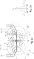
- Fig. 2a illustrates another example of an inventive apparatus 100 for carrying out the inventive method. For simplicity, only the interior of the cryostat is shown, and only the major differences with respect to Fig. 1 are explained.
- the HTS superconductor 3 is guided by current exchange elements 12a, 12b and voltage pick-up elements 15a, 15b through the cleavage 18 of the magnetic field generation device 17.
- the electric line 16a which is connected to the first voltage pick-up element 15a, is guided through the cleavage 18, in close vicinity and parallel to the HTS superconductor 3.
- the electric line 16a is guided to the top, in close vicinity of and in parallel with (or alternatively twisted with) the electric line 16b, which is connected to the second voltage pick-up element 15b.
- field lines 30 of a typical magnetic field generated by the magnetic field generation device 17 are shown.
- Field lines 30 in the central region 23 have a high density, in particular near the magnetic center 31, where the magnetic field strength is highest (and B centr acts on the HTS superconductor 3, typically in a direction perpendicular to the plane/flat side of the tape).
- the field lines 30 have a relatively low density.
- the maximum magnetic field acting on the HTS superconductor there (with corresponding B peri acting on the HTS superconductor 3 at the current exchange elements 12a, 12b, typically in a direction having some inclination to the plane/flat side of the tape) is far below B centr in terms of absolute value.
- the magnetic field strength simply falls off monotonically away from the magnetic center 31.
- the magnetic field often changes its sign several times when going away from the magnetic center 31.
- Such a behavior may be promoted by appropriate magnet design or ferromagnetic screening design.
- FIG. 2b illustrates such a magnetic field (compare axis to the top, illustrating the magnetic flux density B, as a function of location x ⁇ ), and the peripheral regions 24a, 24b and central region 23.
- Fig. 3 illustrates an alternative design of an inventive apparatus 100 for carrying out the inventive method, similar to the apparatus shown in Fig. 2a . Only the major differences are explained.
- the electrical lines 16a, 16b connected to the voltage pick-up elements 15a, 15b both are guided through the cleavage 18 of the magnetic field generation device 17, but only to its center. At its center, the electrical lines 16a, 16b are guided to the top in close vicinity and in parallel to each other (or alternatively twisted) through the magnetic field generation device 17.
- This design has a higher symmetry as compared to the design of Fig. 2a , but requires a feedthrough of lines 16a, 16b through the upper part of the magnetic field generation device ("magnet").
- Fig. 4 illustrates a procedure for measuring the electrical properties of a HTS superconductor as a function of time ⁇ (illustrated to the right), in an i-sweep variant.
- the measurement may be performed, for example, on an apparatus as shown in Fig. 1 .
- the measurement current i (compare full line) applied via the current exchange contacts is varied in a saw-tooth like manner as a function of time ⁇ . Over a period (cycle duration) of here 10 ms, the measurement current i( ⁇ ) is increased linearly from zero to about 3 A here and back to zero. The magnetic field is kept constant.
- the voltage U between the voltage pick-up elements is measured as a function of time, see voltage U( ⁇ ) (compare dashed line).
- the HTS superconductor is practically completely superconducting, and the voltage drop-off is practically zero.
- the measurement current i approaches the critical current (for the given temperature T env and B centr )
- the voltage U increases in an approximately exponential way. Note that the critical current varies locally due to variations in the structure of the HTS superconductor.
- the superconductor has reached its critical current when the voltage U has reached a critical level U cr .
- the momentary measurement current I cj is determined, which is considered as the local critical current (at the magnetic center in the central region of the HTS superconductor at B centr and at T env applied during the measurement).
- an integral ⁇ U ( ⁇ ) d ⁇ can be determined.
- ⁇ 0 being the start of the respective cycle.
- the integral area of ⁇ 0 ⁇ 1 U ⁇ d ⁇ is illustrated with a hatching.
- the first derivative d ⁇ ( ⁇ )/d ⁇ of the probing voltage drop ⁇ ( ⁇ ) may be used for identifying defects in the HTS superconductor passing the characterization zone. In this sense, by smooth and continuous translation of the tape, the time ⁇ corresponds to a tape coordinate x in the longitudinal direction.
- the latter integral allows to take into account the entire voltage drop including minor drops occurring in the areas with reduced flux density. In this way, improved precision of characterization may be achieved.
- Fig. 7 shows a typical first derivative d ⁇ ( ⁇ )/d ⁇ as a function of time during passing of a defect.
- a maximum 71 can be observed, and when the defect leaves the characterization zone, a minimum 72 can be observed.
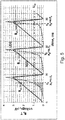
- Fig. 5 illustrates an alternative procedure for measuring the electrical properties of a HTS superconductor as a function of time ⁇ (illustrated to the right), in a B-sweep variant.
- the measurement may be performed, for example, on an apparatus as shown in Fig. 1 .
- the magnetic field applied via the magnetic field generation device is varied in a saw-tooth like manner as a function of time ⁇ .
- cycle duration 10 ms
- the magnetic flux density B( ⁇ ) (taken at the magnetic center, so B corresponds to B centr ) is increased linearly from zero to about 3 Tesla and back to zero here (compare full line).
- the measurement current is kept constant.
- the voltage U between the voltage pick-up elements is measured as a function of time, see voltage U( ⁇ ) (compare dashed line).
- the HTS superconductor is practically completely superconducting, and the voltage drop-off U is practically zero.
- the voltage U increases in an approximately exponential way. Note that the critical magnetic flux density varies locally due to variations in the structure of the HTS superconductor.
- the superconductor has reached its critical magnetic flux density when the voltage U has reached a critical level U cr .
- the momentary magnetic flux density B cj is determined, which is considered as the local critical magnetic flux density (at the given measurement current and T env applied during the measurement).
- a table of critical magnetic flux densities B cj as a function of location x j can be obtained.
- the critical magnetic flux density may be converted into a corresponding critical current density by appropriate predefined functions.
- an integral ⁇ U ( ⁇ ) d ⁇ can be determined.
- ⁇ 0 being the start of the respective cycle.
- the integral area of ⁇ 0 ⁇ 1 U ⁇ d ⁇ is illustrated with a hatching.
- I centr crit (x) is typically transformed into a critical current I HFLT crit present at a magnetic flux density B high , which is typically about 10 Tesla or more, i.e. much larger than B centr , and at a temperature T low , which is typically at 4.2 K or below, i.e. much lower than T env .
- predefined translation functions may be used, for example applying a lift factor that expresses a ratio of critical currents measured at different fields and temperatures.
- This procedure is simplified via a reliable correlation of I c values at B>5T, 4.2 K, where the correlation follows so called alpha-law, i.e. I c ⁇ B -alpha where alpha is a known constant for wide field range.
- Fig. 6 illustrates by way of example another procedure for determining the electrical properties of a HTS superconductor according to the invention.
- the procedure may be performed, in particular, on an inventive apparatus as illustrated in Fig. 1 .
- the measurement current i is measured as a function of time ⁇ during continuous translation of the HTS superconductor.
- the magnetic flux density is fixed here, and the measurement current at the current exchange elements is controlled such that a voltage drop at the voltage pick-up elements, i.e. across the central region, is kept constant at a predefined value U target .
- the control algorithm includes increasing the measurement current i if the momentary voltage U is below U target , and reducing the measurement current i if the momentary voltage U is above U target ; typically a PD-control (proportional-differential control) is applied.
- the time for determining the momentary voltage U, comparing it with U target , deriving an adapted measurement current i such that U will be at U target again and setting this measurement current i at the current exchange elements defines the cycle duration here.
- the measurement current i typically stays practically constant at a high level 60.
- said high level is close to the critical current I centr crit for the given magnetic field strength and temperature T env .
- the measurement current i drops to a significantly lower level 61.
- the present invention proposes to evaluate the electrical properties, in particular the critical current, of a HTS superconductor (3), in particular of coated conductor tape type, wherein a measurement current (i) is injected into an active part/characterization zone (4) of the HTS superconductor, wherein the active part is cooled, but not reservoirs (1, 2) of the HTS superconductor from and to which the HTS superconductor is wound continuously, and exposing only a fraction of the active part to a magnetic field for testing the electrical properties, with the magnetic field for testing having 1.5 T or more, in particular 2 T or more, and typically being oriented perpendicular to a tape flat side, wherein protection means/buffer devices (20a, 20b) are provided against current sharing with respect to outside the active part, wherein injection of the measurement current is done where the residual magnetic field is at least 3 times lower as compared to the magnetic field for testing and/or the local critical current at the current injection locations is at least three times higher as compared to the critical current at the magnetic field for testing.
- current injection is done where the magnetic field has an opposite sign as compared to the magnetic field of testing.
- Evaluation of the electrical properties may be done by determining an integral of a voltage drop (U) across the active part or a fraction of the active part, e.g. between two voltage pick-up elements (15a, 15b), as a function of measurement time ( ⁇ ), in particular comparing the integral value to a critical value (CV) and determining the corresponding time when the critical value was reached.
- U voltage drop
- ⁇ measurement time
- CV critical value
- this defect When this defect reaches high field zone (central region), it will cause a constant addition to the voltage drop until the defect come out of high field zone. Additionally this defect will contribute to measured voltage drop when it passes the through the transient zones (peripheral regions) with field gradient.
- these effects may be taken into account using a first time (or coordinate) derivative from the voltage drop or the integral voltage drop; note that the voltage drop or integral voltage drop has to be examined at identical boundary conditions, such as at identical magnetic field strength and measurement current strength, e.g. at identical relative points during measurement cycles, in each case. For example, there is a stepwise increase of voltage drop with a positive peak of first derivative when local defect enters the characterization zone. Accordingly, there is a stepwise reduction of voltage drop with a negative peak of the first derivative when defect comes out of the characterization zone with high magnetic field.
Landscapes
- Physics & Mathematics (AREA)
- Condensed Matter Physics & Semiconductors (AREA)
- General Physics & Mathematics (AREA)
- Superconductors And Manufacturing Methods Therefor (AREA)
- Testing Electric Properties And Detecting Electric Faults (AREA)
- Investigating Or Analyzing Materials By The Use Of Electric Means (AREA)
Priority Applications (3)
| Application Number | Priority Date | Filing Date | Title |
|---|---|---|---|
| EP18213831.3A EP3671247A1 (de) | 2018-12-19 | 2018-12-19 | Verfahren zur bewertung der elektrischen eigenschaften eines hts-supraleiters |
| JP2019216989A JP2020126039A (ja) | 2018-12-19 | 2019-11-29 | Hts超伝導体の電気特性を評価する方法 |
| US16/720,292 US20200200841A1 (en) | 2018-12-19 | 2019-12-19 | Method for evaluating the electrical properties of a hts superconductor |
Applications Claiming Priority (1)
| Application Number | Priority Date | Filing Date | Title |
|---|---|---|---|
| EP18213831.3A EP3671247A1 (de) | 2018-12-19 | 2018-12-19 | Verfahren zur bewertung der elektrischen eigenschaften eines hts-supraleiters |
Publications (1)
| Publication Number | Publication Date |
|---|---|
| EP3671247A1 true EP3671247A1 (de) | 2020-06-24 |
Family
ID=64746040
Family Applications (1)
| Application Number | Title | Priority Date | Filing Date |
|---|---|---|---|
| EP18213831.3A Withdrawn EP3671247A1 (de) | 2018-12-19 | 2018-12-19 | Verfahren zur bewertung der elektrischen eigenschaften eines hts-supraleiters |
Country Status (3)
| Country | Link |
|---|---|
| US (1) | US20200200841A1 (de) |
| EP (1) | EP3671247A1 (de) |
| JP (1) | JP2020126039A (de) |
Families Citing this family (2)
| Publication number | Priority date | Publication date | Assignee | Title |
|---|---|---|---|---|
| CN113359072B (zh) * | 2020-10-26 | 2025-02-14 | 核工业西南物理研究院 | 一种高温超导带材磁场角度依赖性与扭转测试装置及方法 |
| US20240151787A1 (en) * | 2022-11-03 | 2024-05-09 | The Florida State University Research Foundation, Inc. | Force magnetometer for reel-to-reel assessment of superconducting tapes |
Citations (4)
| Publication number | Priority date | Publication date | Assignee | Title |
|---|---|---|---|---|
| EP1760479A2 (de) * | 2005-09-06 | 2007-03-07 | International Superconductivity Technology Center, The Juridical Foundation | Vorrichtung und Verfahren zur kontinuierlichen Überwachung von magnetischer Flussverteilung |
| US20070149411A1 (en) | 2005-12-28 | 2007-06-28 | Superpower, Inc. | Method of facilitating superconducting tape manufacturing |
| US20100026292A1 (en) * | 2006-07-25 | 2010-02-04 | Los Alamos National Security, Llc | Method and apparatus for measuring magnetic anisotropy of a conductive wire or tape |
| US20120249171A1 (en) * | 2009-09-10 | 2012-10-04 | Basf Se | Method and device for the quality control of superconducting bands |
-
2018
- 2018-12-19 EP EP18213831.3A patent/EP3671247A1/de not_active Withdrawn
-
2019
- 2019-11-29 JP JP2019216989A patent/JP2020126039A/ja active Pending
- 2019-12-19 US US16/720,292 patent/US20200200841A1/en not_active Abandoned
Patent Citations (4)
| Publication number | Priority date | Publication date | Assignee | Title |
|---|---|---|---|---|
| EP1760479A2 (de) * | 2005-09-06 | 2007-03-07 | International Superconductivity Technology Center, The Juridical Foundation | Vorrichtung und Verfahren zur kontinuierlichen Überwachung von magnetischer Flussverteilung |
| US20070149411A1 (en) | 2005-12-28 | 2007-06-28 | Superpower, Inc. | Method of facilitating superconducting tape manufacturing |
| US20100026292A1 (en) * | 2006-07-25 | 2010-02-04 | Los Alamos National Security, Llc | Method and apparatus for measuring magnetic anisotropy of a conductive wire or tape |
| US20120249171A1 (en) * | 2009-09-10 | 2012-10-04 | Basf Se | Method and device for the quality control of superconducting bands |
Non-Patent Citations (1)
| Title |
|---|
| L. ROSSI ET AL.: "Sample and length-dependent variability of 77 and 4.2 K properties in nominally identical RE123 coated conductors", SUPERCONDUCTOR SCIENCE AND TECHNOLOGY, vol. 29, no. 5, 2016, pages 054006, XP020302073, DOI: doi:10.1088/0953-2048/29/5/054006 |
Also Published As
| Publication number | Publication date |
|---|---|
| US20200200841A1 (en) | 2020-06-25 |
| JP2020126039A (ja) | 2020-08-20 |
Similar Documents
| Publication | Publication Date | Title |
|---|---|---|
| US6034527A (en) | Method and measuring apparatus for a contactless longitudinal and transversal homogeneity examination of critical current density in superconductor tape | |
| US7545143B2 (en) | Superconductor probe coil for NMR apparatus | |
| Zhou et al. | Quench Detection Criteria for YBa2Cu3O7‐δ Coils Monitored via a Distributed Temperature Sensor for 77 K Cases | |
| CN105301093A (zh) | 一种超导线圈缺陷位置检测系统 | |
| US20200200841A1 (en) | Method for evaluating the electrical properties of a hts superconductor | |
| Marchevsky et al. | Advancing superconducting magnet diagnostics for future colliders | |
| Tosaka et al. | Project overview of HTS magnet for ultra-high-field MRI system | |
| US5218296A (en) | Method and apparatus for determining at least one characteristic of a superconductive film | |
| JPH0823550B2 (ja) | 超伝導材料の超伝導性を評価する装置及び方法 | |
| Barzi et al. | Test of superconducting wires and rutherford cables with high specific heat | |
| Kim et al. | Experimental study on the accuracy of the proposed LFAC method for measuring the contact resistance of NI HTS coils | |
| Wang et al. | Detecting and describing the inhomogeneity of critical current in practical long HTS tapes using contact-free method | |
| Tsuda et al. | Suitable excitation condition in overshooting process for suppressing magnetic field attenuation in Y-based coated conductor coils | |
| US6452375B1 (en) | Apparatus for measurement of critical current in superconductive tapes | |
| Ilyin et al. | Stability and quench development study in small HTSC magnet | |
| Billan et al. | Test of 1 m long model magnets for LHC | |
| JPH0820418B2 (ja) | 非接触による電流密度測定プローブ | |
| US3428891A (en) | Method for evaluating the stability and operating characteristics of composite superconductors | |
| JP3996830B2 (ja) | 超電導線材の臨界電流特性を測定する方法および装置 | |
| Sampson et al. | Normal state resistance and low temperature magnetoresistance of superconducting cables for accelerator magnets | |
| Vojenčiak et al. | Influence of the voltage taps position on the self-field DC and AC transport characterization of HTS superconducting tapes | |
| Walker et al. | Alternating field losses in mixed matrix multifilament superconductors | |
| JPH08222426A (ja) | 超電導磁石の巻線構造 | |
| CN118033501B (zh) | 一种消除约瑟夫结阵器件冻结磁通的方法和系统 | |
| Baudouy et al. | AC loss measurement of the 45-T hybrid/CIC conductor |
Legal Events
| Date | Code | Title | Description |
|---|---|---|---|
| PUAI | Public reference made under article 153(3) epc to a published international application that has entered the european phase |
Free format text: ORIGINAL CODE: 0009012 |
|
| STAA | Information on the status of an ep patent application or granted ep patent |
Free format text: STATUS: THE APPLICATION HAS BEEN PUBLISHED |
|
| AK | Designated contracting states |
Kind code of ref document: A1 Designated state(s): AL AT BE BG CH CY CZ DE DK EE ES FI FR GB GR HR HU IE IS IT LI LT LU LV MC MK MT NL NO PL PT RO RS SE SI SK SM TR |
|
| AX | Request for extension of the european patent |
Extension state: BA ME |
|
| STAA | Information on the status of an ep patent application or granted ep patent |
Free format text: STATUS: THE APPLICATION IS DEEMED TO BE WITHDRAWN |
|
| 18D | Application deemed to be withdrawn |
Effective date: 20210112 |