EP3671563A1 - Herstellungsverfahren einer metallischen chipkarte, bevorzugt mit relaisantenne - Google Patents
Herstellungsverfahren einer metallischen chipkarte, bevorzugt mit relaisantenne Download PDFInfo
- Publication number
- EP3671563A1 EP3671563A1 EP18306795.8A EP18306795A EP3671563A1 EP 3671563 A1 EP3671563 A1 EP 3671563A1 EP 18306795 A EP18306795 A EP 18306795A EP 3671563 A1 EP3671563 A1 EP 3671563A1
- Authority
- EP
- European Patent Office
- Prior art keywords
- antenna
- card
- spiral
- cavity
- insert
- Prior art date
- Legal status (The legal status is an assumption and is not a legal conclusion. Google has not performed a legal analysis and makes no representation as to the accuracy of the status listed.)
- Withdrawn
Links
Images

Classifications
-
- G—PHYSICS
- G06—COMPUTING OR CALCULATING; COUNTING
- G06K—GRAPHICAL DATA READING; PRESENTATION OF DATA; RECORD CARRIERS; HANDLING RECORD CARRIERS
- G06K19/00—Record carriers for use with machines and with at least a part designed to carry digital markings
- G06K19/06—Record carriers for use with machines and with at least a part designed to carry digital markings characterised by the kind of the digital marking, e.g. shape, nature, code
- G06K19/067—Record carriers with conductive marks, printed circuits or semiconductor circuit elements, e.g. credit or identity cards also with resonating or responding marks without active components
- G06K19/07—Record carriers with conductive marks, printed circuits or semiconductor circuit elements, e.g. credit or identity cards also with resonating or responding marks without active components with integrated circuit chips
- G06K19/077—Constructional details, e.g. mounting of circuits in the carrier
- G06K19/07749—Constructional details, e.g. mounting of circuits in the carrier the record carrier being capable of non-contact communication, e.g. constructional details of the antenna of a non-contact smart card
- G06K19/0775—Constructional details, e.g. mounting of circuits in the carrier the record carrier being capable of non-contact communication, e.g. constructional details of the antenna of a non-contact smart card arrangements for connecting the integrated circuit to the antenna
- G06K19/07756—Constructional details, e.g. mounting of circuits in the carrier the record carrier being capable of non-contact communication, e.g. constructional details of the antenna of a non-contact smart card arrangements for connecting the integrated circuit to the antenna the connection being non-galvanic, e.g. capacitive
-
- G—PHYSICS
- G06—COMPUTING OR CALCULATING; COUNTING
- G06K—GRAPHICAL DATA READING; PRESENTATION OF DATA; RECORD CARRIERS; HANDLING RECORD CARRIERS
- G06K19/00—Record carriers for use with machines and with at least a part designed to carry digital markings
- G06K19/06—Record carriers for use with machines and with at least a part designed to carry digital markings characterised by the kind of the digital marking, e.g. shape, nature, code
- G06K19/067—Record carriers with conductive marks, printed circuits or semiconductor circuit elements, e.g. credit or identity cards also with resonating or responding marks without active components
- G06K19/07—Record carriers with conductive marks, printed circuits or semiconductor circuit elements, e.g. credit or identity cards also with resonating or responding marks without active components with integrated circuit chips
- G06K19/077—Constructional details, e.g. mounting of circuits in the carrier
- G06K19/07749—Constructional details, e.g. mounting of circuits in the carrier the record carrier being capable of non-contact communication, e.g. constructional details of the antenna of a non-contact smart card
-
- G—PHYSICS
- G06—COMPUTING OR CALCULATING; COUNTING
- G06K—GRAPHICAL DATA READING; PRESENTATION OF DATA; RECORD CARRIERS; HANDLING RECORD CARRIERS
- G06K19/00—Record carriers for use with machines and with at least a part designed to carry digital markings
- G06K19/06—Record carriers for use with machines and with at least a part designed to carry digital markings characterised by the kind of the digital marking, e.g. shape, nature, code
- G06K19/067—Record carriers with conductive marks, printed circuits or semiconductor circuit elements, e.g. credit or identity cards also with resonating or responding marks without active components
- G06K19/07—Record carriers with conductive marks, printed circuits or semiconductor circuit elements, e.g. credit or identity cards also with resonating or responding marks without active components with integrated circuit chips
- G06K19/077—Constructional details, e.g. mounting of circuits in the carrier
- G06K19/07749—Constructional details, e.g. mounting of circuits in the carrier the record carrier being capable of non-contact communication, e.g. constructional details of the antenna of a non-contact smart card
- G06K19/07773—Antenna details
- G06K19/07794—Antenna details the record carrier comprising a booster or auxiliary antenna in addition to the antenna connected directly to the integrated circuit
-
- H—ELECTRICITY
- H04—ELECTRIC COMMUNICATION TECHNIQUE
- H04B—TRANSMISSION
- H04B5/00—Near-field transmission systems, e.g. inductive or capacitive transmission systems
- H04B5/20—Near-field transmission systems, e.g. inductive or capacitive transmission systems characterised by the transmission technique; characterised by the transmission medium
- H04B5/24—Inductive coupling
Definitions
- the invention relates to the field of contactless smart cards comprising a card body with a high metallic content or commonly called metallic (or metal) card.
- a radiofrequency communication smart card comprising an insert comprising a relay antenna (passive antenna, amplifier or booster) configured so as to be electro-magnetically coupled with an inserted radio frequency module. in a card cavity.
- a relay antenna passive antenna, amplifier or booster
- the invention can envisage a normal non-relay antenna.
- Smart cards can be of the hybrid type (contacts and contactless) or purely contactless (without electrical contact terminal block).
- Smart cards can have a smart card module comprising on an insulating substrate, a radio frequency transponder with the chip and the antenna.
- the radio frequency chip card modules are generally inserted in a cavity of the card body.
- the invention relates more particularly to bank cards comprising a mainly metallic body by volume and / or by mass.
- the patent FR 2743649 describes a smart card module with antenna and / or contact pads which can be incorporated into a card body cavity or which can form an RFID electronic tag.
- the patent EP1031939 (B1 ) describes a radiofrequency card (or contactless) comprising a relay antenna (or passive) wound in the shape of an eight, housed in a card body and electromagnetically or inductively coupled with the antenna of the module.
- the antenna (relay) or passive comprises a narrow coil concentric with the antenna of the module and a wide coil to receive the electromagnetic cham of a reader.
- hybrid radio frequency devices such as contact and contactless cards, comprising a smart card module with contacts incorporated in a card body and connected to an antenna housed in the card body.
- bank cards with metallic elements inserted inside the body of plastic card or external surface of the card body such as aluminum, titanium, gold.
- the metal provides a feeling of heaviness of the card which is very appreciated by the users. It also gives a visible aesthetic appearance which makes it a high-end product for the privileged.
- WO 2018/152218 A1 describes a smart card having metal extending to the edge of the card. In one mode, it includes a metal frame extending along the edge of the card and a radio frequency inlay inside.
- the patent application US 2015/0269477 A1 describes a dual interface hybrid smart card comprising a metal plate placed in a plastic card body, a booster antenna, and an antenna module with contact pads arranged in a cavity of the card body.
- a metal plate can be placed around a peripheral portion of the card body and in the form of an open loop around a relay antenna.
- the invention aims to solve the aforementioned drawbacks.
- the invention consists in a preferred aspect of having the heaviest metal chip cards possible with metal while having good radio frequency performance.
- the invention relates to an electronic chip module structure for a smart card which makes it possible to have good radio frequency performance in two directions. at least (perpendicular to the main plane of the card), even if the card contains a maximum of metal which generally shields the electromagnetic fields from a contactless reader.
- the card may preferably also have a structure satisfying in particular the mechanical strength constraints of the ISO standard for smart cards and other tests of durability over time.
- Such cards can comply in particular with standard ISO 78016 and / or ISO / IEC 14443 or equivalent.
- the invention aims to solve the drawbacks or to satisfy the above-mentioned objectives. It preferably aims to have good radio frequency performance with a card having metal which may or may not extend to the edges of the card.
- the invention may consist in forming a relay antenna in the very thickness of a metal plate with a thickness which may be greater than 200 or 300 ⁇ m.
- the insert can comprise a large metallic mass at the level of the antenna itself since it is formed in the thickness of a metal plate which may have substantially or almost the thickness of a card to standard chip.
- the connection of the radio frequency module with the antenna is facilitated since it uses a relay antenna.
- the module is just fixed to the card, in particular by adhesive without ohmic connection (or soldering) with the relay antenna.
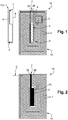
- step 100 (can correspond to step 100 ( fig. 4 ), a first possible step of the method for manufacturing a radiofrequency smart card according to a preferred embodiment is illustrated.
- the card envisaged by the invention is intended to include an insert (or inlay in English).
- this envisaged insert may include a relay antenna (passive or amplifier) which is configured so as to be electromagnetically (or inductively) coupled with a radio frequency module (or transponder).
- a radio frequency module or transponder
- the latter can be inserted into a cavity 3, 3bis of the insert or of the card or positioned at a corresponding location 3.
- the module can be in the form of a tag or RFID tag of fine structure, simply fixed to the card body at location 3 of the module, without being inserted into a cavity.
- the antenna is configured to ensure an inductive coupling or connection with the module, it is not excluded to configure the antenna to have its two ends 2I, (2E, 2D) coming close to the radio frequency module so as to connect in ohmic or capacitive connection.
- its internal end 2I could stop at the edge of the cavity or location 3 of the module.
- its external end 2E or 2F could be brought back with a conductive bridge 6 electrically isolated at the interface with the antenna 2.
- the method can include the step of forming an antenna spiral 12, a cavity 3 (optional but preferred for conventional modules of the smart card type) and a plate capacitor 4 in a metal plate, said spiral comprising an external terminal end and an internal terminal end, at least one forming a first capacitor plate,
- the antenna spiral 12 can be provided in this way or obtained by cutting from a metal plate.
- an antenna pattern 3 (or of a plurality of antenna) is formed in a metal plate in particular by laser cutting.
- Each antenna can be extracted from its metallic base plate, in particular after laminating a covering and / or decoration sheet.
- the plate is here made of steel, but it can be of any known metallic material such as gold, tungsten, silver, aluminum, copper or alloys.
- the cavity 3 can be formed by thinning the thickness of the turns (or thinning the thickness of the metal plate before cutting the turns); It can be obtained by machining or molding in a location 3 indicated by dotted lines on the figure 1 .
- the cavity can be formed by an antenna pattern 2bis which circumvents the location 3 of the cavity.
- the width of the turns is narrower in the area around the cavity.
- the width of the turns can be a few millimeters around the cavity while the turns close to the edge of the card (in particular the outer turn) can be much wider from (0.5 cm or 1 cm) to 2 cm.
- the cavity location 3 includes an opening 3bis passing through the cut metal plate 2.
- the spiral 12 ends at its internal end (terminal end 4) with a metal plate 3 which is obtained in the same way as the antenna turns.
- This plate forms a first capacitor plate which is intended to cooperate with a second capacitor plate 5.
- the method preferably provides for the addition of a second capacitor plate 5 facing at least one of said two end portions 4;
- the second plate extends via an insulated conductive bridge 6 to the other terminal portion 2D, 2E to connect it capacitively or ohmically to form a resonant circuit (RLC).
- RLC resonant circuit
- the method provides for making a PC portion of a conductive metal plate, in particular by cutting from another metal plate.
- the PC portion includes a zone 5 (forming a second capacitor plate) intended to be positioned opposite the first capacitor plate 4. It also includes a zone 6 forming a conductive bridge.
- the entire underside of the PC portion may include an insulator (deposited in particular by material jet, screen printing or other known technique) with the exception of its narrow end 7.
- the second portion PC can be thinned by operation 8 of rectification or milling (or cut from an already thin metal plate before its assembly with the antenna 2).
- a thinning 9 can be provided at the location of the PC portion, indicated in the figure of the second PC portion, can preferably be thinned in particular by milling or the like.
- the assembly of the antenna 2 with the capacitor element PC of the figure 1 is positioned opposite the first plate 4 and connected via its end 7 by electrical welding to an external end 2E of the antenna spiral 12.
- the insulated conductive bridge 6 could be connected, via its end 7, to another adjacent 2D end of the antenna.
- the external coil is sectioned at level "F” on its external transverse side but it could be sectioned at level "D" in the left corner joining the antenna pattern.
- first 4 and second portions 5 of the capacitor plate can be located outside (or at the outer edge) of the spiral 12 (rather than inside the spiral) and be connected capacitively while the end 4 of the central turn is ohmically connected (eg soldering) to one end 5 of the PC plate.
- the PC portion can be placed in the same location, being isolated at the interface with the antenna and forming a capacitive connection.
- the invention according to this preferred embodiment provides for a step 110 intended to keep the turns 2 well spaced from one another.
- the method can provide for the insertion of insulating material between the turns 2 of the antenna spiral 12 in particular by hot or cold lamination (or rolling) or by distributing polymerizable fluid insulating material between the turns.
- This step of holding the turns in place with respect to each other can be carried out before step 120 of adding the capacitor plate PC or after.
- the method may provide for laminating or hot pressing at least one thermoplastic or hot-melt sheet on the antenna.
- the fluidized material flows between the turns and then hardens on cooling.
- the antenna spiral 12 can extend to the edge of the card. This characteristic can be obtained after extraction of the antenna from a large format plate containing a plurality of cut antenna.
- the antenna can be completely embedded in insulating material (for example overmolded).
- the antenna can be extracted from a plate to be deposited inside an insulating frame arranged on an insulating substrate having a larger surface than the antenna then a sheet and / or resin is deposited on the antenna to carry out a lamination.
- each insert can be covered with at least one sheet or insulating covering layer on each main face.
- the antenna can receive in the cavity a radio frequency module (not shown) which conventionally comprises an antenna L1 on an insulating support connected to a radio frequency chip, if necessary, a tuning capacity can be included in the radio frequency chip.
- the module can only be of the contactless type or of the hybrid contact and contactless type. In all preferred cases (in particular for reasons of performance or ease of assembly or connection of the radio frequency module), the module can be inductively coupled with the relay antenna.
- the radio frequency module can be inserted into the cavity 3 before or after the addition of cover and / or finish sheets (from step 130).
- the method performs a rolling of sheets on the insert, the cavity 3 ( fig. 3 ) or the inter turn space may have been filled with resin.
- the method performs cavity machining 3 before inserting the antenna module (not shown).
- the module is thus in coupling position with the insert comprising a relay or passive type antenna (RLC circuit) which provides an extension of the radio frequency communication range of the antenna module (or radio frequency communication transponder).
- the relay antenna R comprises the RLC circuit formed by the spiral 12 (inductance L), and the capacitor 4, 5 (C); Resistance 5 is implicit.
- the antenna spiral can have a thickness of between 300 and 700 ⁇ m.
- the turns can be at least as wide in the plane of the card as high in the direction perpendicular to this plane.
- the turns can be fine in particular around the module (a few hundred microns, or even 1 mm to a few millimeters) and wide at least at the level of the external turn of the order of 0.5 cm from 1 cm.
- the card body plate may comprise an assembly of metal plates welded together or assembled by means of a thin adhesive layer. This last assembly can improve the mechanical resistance of bending / torsion.
- the external turn can have a greater width than the other turns.
- the width can be for example from 0.5 to 1 cm so as to have more mass at the edge.
Landscapes
- Engineering & Computer Science (AREA)
- Microelectronics & Electronic Packaging (AREA)
- Computer Hardware Design (AREA)
- Physics & Mathematics (AREA)
- General Physics & Mathematics (AREA)
- Theoretical Computer Science (AREA)
- Computer Networks & Wireless Communication (AREA)
- Signal Processing (AREA)
- Details Of Aerials (AREA)
- Credit Cards Or The Like (AREA)
Priority Applications (2)
| Application Number | Priority Date | Filing Date | Title |
|---|---|---|---|
| EP18306795.8A EP3671563A1 (de) | 2018-12-21 | 2018-12-21 | Herstellungsverfahren einer metallischen chipkarte, bevorzugt mit relaisantenne |
| PCT/EP2019/084087 WO2020126572A1 (fr) | 2018-12-21 | 2019-12-06 | Procede de fabrication d'une carte a puce metallique, de preference avec antenne relais |
Applications Claiming Priority (1)
| Application Number | Priority Date | Filing Date | Title |
|---|---|---|---|
| EP18306795.8A EP3671563A1 (de) | 2018-12-21 | 2018-12-21 | Herstellungsverfahren einer metallischen chipkarte, bevorzugt mit relaisantenne |
Publications (1)
| Publication Number | Publication Date |
|---|---|
| EP3671563A1 true EP3671563A1 (de) | 2020-06-24 |
Family
ID=65228307
Family Applications (1)
| Application Number | Title | Priority Date | Filing Date |
|---|---|---|---|
| EP18306795.8A Withdrawn EP3671563A1 (de) | 2018-12-21 | 2018-12-21 | Herstellungsverfahren einer metallischen chipkarte, bevorzugt mit relaisantenne |
Country Status (2)
| Country | Link |
|---|---|
| EP (1) | EP3671563A1 (de) |
| WO (1) | WO2020126572A1 (de) |
Cited By (1)
| Publication number | Priority date | Publication date | Assignee | Title |
|---|---|---|---|---|
| RU2789826C1 (ru) * | 2022-04-28 | 2023-02-10 | Олег Умарович Айбазов | Способ производства карт с металлическим слоем и бесконтактным интерфейсом (варианты) |
Families Citing this family (1)
| Publication number | Priority date | Publication date | Assignee | Title |
|---|---|---|---|---|
| CN112749571B (zh) * | 2020-12-28 | 2022-07-05 | 杭州海康威视数字技术股份有限公司 | 读卡终端及无线射频识别系统 |
Citations (7)
| Publication number | Priority date | Publication date | Assignee | Title |
|---|---|---|---|---|
| FR2743649A1 (fr) | 1996-01-17 | 1997-07-18 | Gemplus Card Int | Module electronique sans contact, carte etiquette electronique l'incorporant, et leurs procedes de fabrication |
| EP1031939B1 (de) | 1997-11-14 | 2005-09-14 | Toppan Printing Co., Ltd. | Zusammengesetzte ic-karte |
| US20080246664A1 (en) * | 2007-04-06 | 2008-10-09 | Murata Manufacturing Co., Ltd. | Wireless ic device |
| US20150269477A1 (en) | 2012-08-30 | 2015-09-24 | David Finn | Dual-interface hybrid metal smartcard with a booster antenna or coupling frame |
| FR3032294A1 (fr) * | 2015-02-02 | 2016-08-05 | Smart Packaging Solutions | Carte a puce sans contact a double antenne |
| EP3182336A1 (de) * | 2015-12-14 | 2017-06-21 | Gemalto Sa | Funkfrequenzvorrichtung mit anpassbarem lc-schaltkreis, der ein elektrisches und/oder elektronisches modul umfasst |
| WO2018152218A1 (en) | 2017-02-14 | 2018-08-23 | Cpi Card Group - Colorado, Inc. | Edge-to-edge metal card and production method |
-
2018
- 2018-12-21 EP EP18306795.8A patent/EP3671563A1/de not_active Withdrawn
-
2019
- 2019-12-06 WO PCT/EP2019/084087 patent/WO2020126572A1/fr not_active Ceased
Patent Citations (7)
| Publication number | Priority date | Publication date | Assignee | Title |
|---|---|---|---|---|
| FR2743649A1 (fr) | 1996-01-17 | 1997-07-18 | Gemplus Card Int | Module electronique sans contact, carte etiquette electronique l'incorporant, et leurs procedes de fabrication |
| EP1031939B1 (de) | 1997-11-14 | 2005-09-14 | Toppan Printing Co., Ltd. | Zusammengesetzte ic-karte |
| US20080246664A1 (en) * | 2007-04-06 | 2008-10-09 | Murata Manufacturing Co., Ltd. | Wireless ic device |
| US20150269477A1 (en) | 2012-08-30 | 2015-09-24 | David Finn | Dual-interface hybrid metal smartcard with a booster antenna or coupling frame |
| FR3032294A1 (fr) * | 2015-02-02 | 2016-08-05 | Smart Packaging Solutions | Carte a puce sans contact a double antenne |
| EP3182336A1 (de) * | 2015-12-14 | 2017-06-21 | Gemalto Sa | Funkfrequenzvorrichtung mit anpassbarem lc-schaltkreis, der ein elektrisches und/oder elektronisches modul umfasst |
| WO2018152218A1 (en) | 2017-02-14 | 2018-08-23 | Cpi Card Group - Colorado, Inc. | Edge-to-edge metal card and production method |
Cited By (1)
| Publication number | Priority date | Publication date | Assignee | Title |
|---|---|---|---|---|
| RU2789826C1 (ru) * | 2022-04-28 | 2023-02-10 | Олег Умарович Айбазов | Способ производства карт с металлическим слоем и бесконтактным интерфейсом (варианты) |
Also Published As
| Publication number | Publication date |
|---|---|
| WO2020126572A1 (fr) | 2020-06-25 |
Similar Documents
| Publication | Publication Date | Title |
|---|---|---|
| EP0671705B1 (de) | Herstellungsverfahren einer Kombi-Karte | |
| EP0916144B1 (de) | Herstellungsverfahren für eine transponderspule | |
| FR2721733A1 (fr) | Procédé de fabrication d'une carte sans contact par surmoulage et carte sans contact obtenue par un tel procédé. | |
| EP1428258B1 (de) | Herstellung eines elektronischen etikettes geringer dicke | |
| EP1141887B1 (de) | Verfahren zur herstellung einer kontaktlosen chipkarte | |
| EP4070241B1 (de) | Die erfindung betrifft ein herstellungsverfahren einer funkfrequenz-chipkarte, die eine metallplatte mit einem schlitz in der platte umfasst | |
| EP3391291A1 (de) | Hochfrequenzvorrichtung mit verstellbarer schaltung mit einem elektrischen und/oder elektronischen modul | |
| EP1190377B1 (de) | Verfahren zur herstellung einer tragbaren elektronischen anordnung mit einer integrierten schaltung mit kostengünstigem dielektricum | |
| WO2020126572A1 (fr) | Procede de fabrication d'une carte a puce metallique, de preference avec antenne relais | |
| EP3899792B1 (de) | Herstellungsverfahren einer metallischen funkfrequenz-chipkarte mit verbesserter elektromagnetischer leitfähigkeit | |
| WO2020126573A1 (fr) | Procede de fabrication d'un insert de carte a puce radiofrequence comportant une plaque metallique | |
| EP4028945B1 (de) | Herstellungsverfahren einer metallischen chipkarte mit minirelais-antenne | |
| EP3663984A1 (de) | Herstellungsverfahren einer chipkarte mit verbindung von modulen | |
| WO2021233869A1 (fr) | Procédé de métallisation électro-chimique d'un circuit électrique double-face pour carte à puce et circuit électrique obtenu par ce procédé. | |
| WO2002001495A1 (fr) | Carte hybride a ensemble de contact ohmique et puits delocalises | |
| EP0969410B1 (de) | Chipkarte mit Antenne | |
| WO2020114753A1 (fr) | Procede de fabrication d'une carte a puce metallique ou non avec antenne relais | |
| WO2020127109A1 (fr) | Procede de fabrication d'une carte a puce radiofrequence metallique a permittivite amelioree avec perforations etendues | |
| WO2020099279A1 (fr) | Procede de realisation d'un insert electronique pour support portable multi-composants et insert obtenu | |
| FR2905494A1 (fr) | Dispositif electronique a module a circuit integre et antenne raccordes par des connexions electriques capacitives | |
| EP3427190B1 (de) | Herstellungsverfahren eines chipmoduls eines integrierten schaltkreises, und vorrichtung, die dieses modul umfasst | |
| FR2736453A1 (fr) | Support portable a microcircuit, notamment carte a puce, et procede de fabrication dudit support | |
| FR3030087A1 (fr) | Module pour cartes a microcircuit, cartes a microcircuit comprenant un tel module et procede de fabrication | |
| EP3832546A1 (de) | Herstellungsverfahren einer funkfrequenz-chipkarte, die eine metallplatte mit einem schlitz oder einem spiel in der platte umfasst | |
| FR2893164A1 (fr) | Procede de fabrication d'une carte a micro-circuit, notamment a antenne magnetique. |
Legal Events
| Date | Code | Title | Description |
|---|---|---|---|
| PUAI | Public reference made under article 153(3) epc to a published international application that has entered the european phase |
Free format text: ORIGINAL CODE: 0009012 |
|
| STAA | Information on the status of an ep patent application or granted ep patent |
Free format text: STATUS: THE APPLICATION HAS BEEN PUBLISHED |
|
| AK | Designated contracting states |
Kind code of ref document: A1 Designated state(s): AL AT BE BG CH CY CZ DE DK EE ES FI FR GB GR HR HU IE IS IT LI LT LU LV MC MK MT NL NO PL PT RO RS SE SI SK SM TR |
|
| AX | Request for extension of the european patent |
Extension state: BA ME |
|
| STAA | Information on the status of an ep patent application or granted ep patent |
Free format text: STATUS: THE APPLICATION IS DEEMED TO BE WITHDRAWN |
|
| 18D | Application deemed to be withdrawn |
Effective date: 20210112 |