EP3671564A1 - Herstellungsverfahren eines einsatzes einer funkfrequenz-chipkarte, der eine metallplatte umfasst - Google Patents
Herstellungsverfahren eines einsatzes einer funkfrequenz-chipkarte, der eine metallplatte umfasst Download PDFInfo
- Publication number
- EP3671564A1 EP3671564A1 EP18306797.4A EP18306797A EP3671564A1 EP 3671564 A1 EP3671564 A1 EP 3671564A1 EP 18306797 A EP18306797 A EP 18306797A EP 3671564 A1 EP3671564 A1 EP 3671564A1
- Authority
- EP
- European Patent Office
- Prior art keywords
- module
- plate
- antenna
- loop
- radio frequency
- Prior art date
- Legal status (The legal status is an assumption and is not a legal conclusion. Google has not performed a legal analysis and makes no representation as to the accuracy of the status listed.)
- Withdrawn
Links
Images


Classifications
-
- G—PHYSICS
- G06—COMPUTING OR CALCULATING; COUNTING
- G06K—GRAPHICAL DATA READING; PRESENTATION OF DATA; RECORD CARRIERS; HANDLING RECORD CARRIERS
- G06K19/00—Record carriers for use with machines and with at least a part designed to carry digital markings
- G06K19/06—Record carriers for use with machines and with at least a part designed to carry digital markings characterised by the kind of the digital marking, e.g. shape, nature, code
- G06K19/067—Record carriers with conductive marks, printed circuits or semiconductor circuit elements, e.g. credit or identity cards also with resonating or responding marks without active components
- G06K19/07—Record carriers with conductive marks, printed circuits or semiconductor circuit elements, e.g. credit or identity cards also with resonating or responding marks without active components with integrated circuit chips
- G06K19/077—Constructional details, e.g. mounting of circuits in the carrier
- G06K19/07749—Constructional details, e.g. mounting of circuits in the carrier the record carrier being capable of non-contact communication, e.g. constructional details of the antenna of a non-contact smart card
- G06K19/0775—Constructional details, e.g. mounting of circuits in the carrier the record carrier being capable of non-contact communication, e.g. constructional details of the antenna of a non-contact smart card arrangements for connecting the integrated circuit to the antenna
-
- G—PHYSICS
- G06—COMPUTING OR CALCULATING; COUNTING
- G06K—GRAPHICAL DATA READING; PRESENTATION OF DATA; RECORD CARRIERS; HANDLING RECORD CARRIERS
- G06K19/00—Record carriers for use with machines and with at least a part designed to carry digital markings
- G06K19/06—Record carriers for use with machines and with at least a part designed to carry digital markings characterised by the kind of the digital marking, e.g. shape, nature, code
- G06K19/067—Record carriers with conductive marks, printed circuits or semiconductor circuit elements, e.g. credit or identity cards also with resonating or responding marks without active components
- G06K19/07—Record carriers with conductive marks, printed circuits or semiconductor circuit elements, e.g. credit or identity cards also with resonating or responding marks without active components with integrated circuit chips
- G06K19/077—Constructional details, e.g. mounting of circuits in the carrier
- G06K19/07749—Constructional details, e.g. mounting of circuits in the carrier the record carrier being capable of non-contact communication, e.g. constructional details of the antenna of a non-contact smart card
- G06K19/07773—Antenna details
- G06K19/07794—Antenna details the record carrier comprising a booster or auxiliary antenna in addition to the antenna connected directly to the integrated circuit
-
- H—ELECTRICITY
- H01—ELECTRIC ELEMENTS
- H01Q—ANTENNAS, i.e. RADIO AERIALS
- H01Q1/00—Details of, or arrangements associated with, antennas
- H01Q1/12—Supports; Mounting means
- H01Q1/22—Supports; Mounting means by structural association with other equipment or articles
- H01Q1/225—Supports; Mounting means by structural association with other equipment or articles used in level-measurement devices, e.g. for level gauge measurement
-
- H—ELECTRICITY
- H01—ELECTRIC ELEMENTS
- H01Q—ANTENNAS, i.e. RADIO AERIALS
- H01Q13/00—Waveguide horns or mouths; Slot antennas; Leaky-waveguide antennas; Equivalent structures causing radiation along the transmission path of a guided wave
- H01Q13/02—Waveguide horns
Definitions
- the invention relates to the field of contactless smart cards having a high metallic content or comprising a metallic plate which can preferably extend up to at least one edge of the card.
- Smart cards can be of the hybrid type (contacts and contactless) or purely contactless (without terminal block for electrical contacts 5).
- the plate is in principle included in an insert covered by at least one sheet or external covering film.
- Smart cards can have a smart card module comprising a radiofrequency transponder (or chip) (with the chip and the antenna) carried on an insulating substrate of the module.
- the radio frequency chip card modules are generally inserted in a cavity of the card body. They can also connect an antenna housed in the card body via electrical interconnection elements, connecting terminal areas of the antenna to connection areas of the chip placed on the module.
- a smart card radio frequency module can be coupled with a passive antenna or relay housed in the card body.
- the invention relates more particularly to metallic bank, payment and transport cards.
- the patent FR 2743649 describes a smart card module with antenna and / or contact pads which can be incorporated into a card body cavity or that can form an electronic RFID tag.
- hybrid radio frequency devices such as contact and contactless cards, comprising a smart card module with contacts incorporated in a card body and connected to an antenna housed in the card body.
- bank cards comprising metal elements in the insert inside the plastic card body or on the external surface of the card body such as aluminum, titanium, gold.
- the metal provides a feeling of heaviness of the card which is very appreciated by the users. It also gives a visible aesthetic appearance which makes it a high-end product for the privileged.
- the patent application US2015 / 0269477 A1 describes a metallic chip card of the “booster” type comprising a metal plate, a receiving cavity of an antenna module, with radio frequency chip.
- the plate forms an open loop which contributes to the communication of the antenna module.
- the invention aims to solve the aforementioned drawbacks.
- the invention relates to an electronic chip module structure for a smart card which makes it possible to have good radio frequency performances RF card in all directions, even if the card contains a maximum of metal to inside or above or on the edge or periphery of the card.
- the card should preferably also have a structure satisfying the mechanical strength constraints in terms of ISO standard for smart cards, other tests in particular of durability over time.
- the invention consists, according to a preferred aspect, of having the heaviest metal chip cards possible while having good radiofrequency performance.
- the invention consists in forming the metal plate in the form of an antenna turn with the least possible cutting or possible metal loss and to complete the loop with other complementary turns, if necessary.
- the invention allows a heavy metal card easy to manufacture and having good radio frequency communication performance.
- a first metal insert is illustrated, for a radio frequency 1A smart card, in progress, in accordance with steps of a first embodiment or implementation of the method of the invention.
- the method may include steps of supplying at least one metal plate cut out in the form of an antenna loop and having a cutout in a reception area of a radio frequency module.
- this mode can provide a metal plate 2 having a format equal to that of a smart card or preferably a plurality of large metal plates from which the subsequently cut inserts will be extracted.
- Any metal can be used among others steel, gold, tungsten, aluminum or metal alloys.
- the thickness of the plate can correspond to the final thickness of a standard card, ie 0.76 mm.
- the thickness of the plate 2 can also be obtained by subtracting from this thickness of 0.76 mm the thicknesses of the final covering and / or decoration layers to be laminated over.
- the thickness of the plate can be variable depending on the scenario, for example, it can be approximately 400 to 700 ⁇ m for assembly with other insulating or metallic sheets or layers.
- Plate 2 can be formed from several metal plates or layers.
- the plate 2 may comprise layers of precious material (gold, silver) fixed in sheet or in plating or by electrochemical deposition such as for example surface treatments of the contact areas of the smart card module.
- Each plate 2 comprises a slot J, passing through the thickness of the plate which is located at the edge of the plate and which can match the short side of the smart card near a smart card M1 module slot (not shown).
- the plate 2 also has an opening 11, also passing through the thickness of the plate 2, and positioned around the location of a smart card module.
- the opening 11 communicates here with the slot J.
- the method comprises the step of producing two interconnection terminal ends 4, 5 intended to connect a radiofrequency module M1.
- the two terminal interconnection ends 4, 5 of the plate 2 are made at the edge of the slot J.
- the plate has continuous portions of unequal width which bypass the cavity 11 from one end 4 to the other 5.
- the plate is configured so as to form an open loop (in the unconnected or not completed state) with two free ends 4 and 5 (before connection).
- the plate 2 thus has a single turn (or loop) 2s which can have several widths.
- These ends 4, 5 are intended to electrically connect a smart card module of conventional type comprising a radio frequency chip of which only the location 12 is illustrated.
- the method comprises a step of forming at least one antenna turn or antenna circuit (which may include resistance, capacitance, interconnection pads, coils, etc.) extending or completing at least said loop 2s.
- at least one antenna turn or antenna circuit which may include resistance, capacitance, interconnection pads, coils, etc.
- the invention provides at least two embodiments ( figs. 1 or 2 ) or ( fig. 3B ).
- an additional antenna circuit "CC1" (comprising all or part of the elements 8, 6, 7, 9, 10: fig. 1 ) can be produced on an extended substrate covering 3 the body of the insert;
- an additional antenna circuit "CC2” (comprising all or part of the elements 16, 18, 19, 20, 17: fig. 3B ) can be produced on a module substrate 3B, the extent (or surface) of which is smaller since it only corresponds to the surface of the opening 11 or of the cavity 12.
- the antenna circuit CC1 or CC2 is connected to the loop 2s of the metal plate 2 in order to extend it by ohmic and / or capacitive contact.
- the antenna circuit can be produced on a substrate 3 which then covers or supports the entire plate 2.
- the complementary antenna circuit (comprising the antenna turns 16) can be produced on a metallized insulating substrate (or lead frame) 3B forming a module M2 which is then inserted in an opening 11, or at least one cavity 12.
- the method of the invention can provide for connecting the aforementioned M2 module by means of a capacitive and / or ohmic connection (eg by contact or electrical welding) of said radio frequency module at the terminal ends of said loop. antenna.
- interconnection pads 6, 7 can be produced at least in part or in whole outside of the plate 2, in particular on a substrate 3.
- these areas 6, 7 are produced on an insulating substrate 3 made of plastic material in particular PVC or other material (PC, PET, etc.) and which can preferably be assembled beforehand to the plate 2, without being an obligation.
- plastic material in particular PVC or other material (PC, PET, etc.) and which can preferably be assembled beforehand to the plate 2, without being an obligation.
- the method performs on the substrate 3 a complementary circuit comprising at least one or more antenna turns 8 which extend (s) or naturally complete the loop 2s of the plate 2.
- At least one antenna turn can be formed on an insulating sheet 3 assembled or intended to be assembled with said metal plate 2p.
- the turns 8 can be made by inlaying a conductive wire with a starting point 9 close to one end 5 of the loop 2s and an ending point 10 close to the other end 4.
- the turns 8 can form, after a few turns or loops, a module interconnection range 7 on the substrate 3 in a known manner, for example by forming zigzags 7 of embedded wire.
- connection point 10 The other end 4 of the loop 2 is connected by a connection point 10 directly to an interconnection pad 6 (produced as for 7 on the substrate), via an insulated (or sheathed) wire bridge 13.
- the complementary antenna circuit "CC1" and the interconnection pads to the module can be produced by electrochemical etching or other known method such as jet of conductive material, etc.
- connections of tracks 6, 7 to points 9 or 10 can be made by thermocompression, welded wire. Where appropriate, the zones comprising the connection points 9, 10 can be thinned themselves and on the passage of the conductive wires or bridges 13 or at the welds on the plate 2p or to avoid excess thicknesses at the level of the metal plate .
- the entire antenna circuit with the connection pads 9, 10, the turns 8, the module interconnection pads can be produced first on the substrate 3, before the metal plate 2p is carried over, then the metal plate 2p is transferred to the sheet 3 and the antenna circuit 8, so as to connect the connection points 9 and 10 of the antenna to the ends 4 and 5 respectively.
- Points 9 and 10 may preferably be below the ends 4 and 5 unlike the illustration in the figure 1 if they are made on the substrate 3)
- the method can provide for placing a binder conductive material, in the form of a film (ACF) or an anisotropic paste (ACP) between the ends 4, 5 and the antenna connection points arranged on the substrate or a other conductive glue.
- ACF film
- ACP anisotropic paste
- the connection can also be made by simple electrical contact.
- the insert 1A thus formed can receive a purely contactless radio frequency module connected to pads 6 and 7, a filling resin to fill the slot J and / or the opening 11 around the module or possibly also over the module, before receiving one or more cover sheet (s) by lamination on one side opposite sheet 3 or on two opposite sides.
- the insert may not receive a cover sheet, the thickness of the metal plate corresponding to the standardized thickness of the smart card.
- the invention can provide for filling the cavity and the slot J with a plastic or thermoplastic resin or ultraviolet polymerizing material, then covering the insert with at least one or more cover and / or finish sheets, at least on the side of the opening 11 (opposite the substrate) or on both sides.
- the method can provide for machining a module receiving cavity 8 until the interconnection pads 6 and 7 are updated. Then, the hybrid module (not illustrated) can be inserted in the conventional manner and connected to the pads. interconnection 6 and 7 at the same time.
- the module M can be a module with antenna and radio frequency chip;
- This module M can be configured so as to form an antenna module for booster antenna (or relay) formed by the single loop 2s of the plate 2p and the antenna circuit complement (CC1, 8).
- the turns 8 can be inductively coupled with turns of the module M.
- An additional capacitor to form an RLC circuit can be produced by crossing the antenna wire 8 on the path of the turns 8 in the opening 11.
- a capacitor plate (or metallization) 14 can be formed facing tracks 6 and 7 on the face of the substrate opposite to that carrying tracks 6 and 7. These tracks 6 and 7 can therefore act as a capacitor by being associated with a metallized surface 14 arranged opposite.
- the metal plate 2p belongs to a spiral (or coil) of closed antenna (2s, 8) composed of the loop 2s supplemented by other turns 8.
- the spiral (2s with 8) is closed at the slot J by the turns 8.
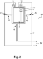
- the object of the figure 2 is identical to that of the figure 1 with the exception of the addition of at least one slot 15 opening into the opening 15.
- the plate antenna loop 2s comprises at least one slot 15 formed in the metal plate;
- the slot 15 opens into the opening 11 of the plate and extends only partially over the width of the loop 2s without opening beyond the periphery of the plate 2p.
- the slot 15 is reducing the width or the section of the loop, and is held back from the peripheral edge of the plate or of the loop).
- This slot 15 (or several slots 15 arranged perpendicular to each edge of the plate) seems to allow a better channeling of the current and concentration of the flow of the current towards the outside of the plate.
- An induced current passage (or a section of plate) with a thickness E1 or E2 is maintained at the edge of the plate.
- the slots 15 also make it possible to “tuner” or adjust the antenna circuit on the wire (or loop 2s) whose section corresponds to the section of the plate, by modifying its RLC properties.
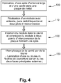
- a third smart card insert is illustrated during production in accordance with a third preferred embodiment of the invention. It is described in relation to the steps described figure 4 .
- step 100 a large antenna turn 2s and a cavity (or opening) 12 are formed in a metal plate 2p;
- Reference 2 is equivalent to a metal plate 2p and / or a loop (or turn) 2s associated or belonging to an antenna circuit CC1 or CC2 comprising the coil 8 or 16.
- the plate can be substantially like that of the figure 1 , with the difference that the opening 3 may be more reduced in surface area and may or may not correspond to the surface area or size of a standard smart card module with an antenna carried thereon;
- the plate here comprises (in place of the opening 11, a cavity 12 of module M2.
- the cavity 12 can form a plane P1 for receiving the module, using two interconnection shoulders 25, 26 arranged therein in extension of the connection ends 4, 5 of the loop 2s.
- the shoulders 25, 26 each have an upper interconnection face located below the main face 27 of the metal plate and at a plane P1 of the cavity 12.
- the plane P1 can be reinforced by two other shoulders 29, 30 placed here in the corners of the cavity 12. These shoulders 29, 30 form with the shoulders 25, 26 four support points or support for the module M2.
- the M2 module can be flush with the surface 27 of the metal plate 2p.
- This embodiment has the particular advantage of having a maximum of metal both on the main surface and in plate thickness.
- the loop 2s here forms part of a spiral closed at the level of the slot J by the external coil 31 at the entrance to the cavity 12 for receiving the module M2.
- the M2 module (or spiral 16) can constitute with the loop 2s a relay antenna, the chip being able to be replaced by a frequency tuning capacitor chip.
- the chip forming the capacitor can also be replaced by a capacitor in the form of superimposed plates, in particular on either side of the insulating substrate 3B.
- SMD surface-mounted component
- the module M2 may include contact pads flush with the surface 27 (or on the external surface) once the face 27 of the plate is covered with finishing sheet and / or cover, the chip being of the hybrid type. (contact and contactless).
- the assembly 1B (of the module and of the loop 2s) can comprise an additional module with radio frequency antenna M3 (not illustrated), introduced by the face 32 opposite to the face 27 (the shoulders 25, 26, 29 , 30 can be machined below to form a plane P2 accessible from the rear face 32).
- M3 radio frequency antenna
- This M3 antenna module can be configured so as to be coupled (and boosted, amplified) by the relay antenna described above (including the 2s loop, supplemented by the turns of module 16 and possibly a capacitor in place of the radio frequency chip 17).
- a chip pad connects by soldered wire an internal end of the antenna 16 via a metallization 20, while the other chip pad connects by soldered wire 22 a conductive bridge 21 (on the external face of the substrate or film) through a hole in the substrate or film 3B.
- the bridge passes over the turns 16 and crosses the substrate 3B using a metallized hole 23.
- the chip can also be connected otherwise by being turned over (flip-chip technique)
- step 120 the method comprises a step of inserting the module M2 into the cavity 12 and connecting the module to two interconnection points 25, 26 of the plate 2 forming a turn 2s.
- connection of the module M2 to the loop 2s can be carried out capacitively by placing an insulator between at least one interconnection shoulder 25 or the two shoulders 25, 26 and the terminal ends 18, 19 of the spiral 16.
- an interconnection shoulder 25 can be connected in ohmic manner with the interconnection pad 18 of the antenna 16 while the other shoulder 26 can be connected by ohmic connection.
- the capacitive surfaces can be adapted, configured according to the need for frequency tuning of the antenna circuit 8, 16.
- the method can provide for filling the cavity with plastic or thermoplastic resin or material which is polymerizable with UV ultraviolet rays or other insulating filling material on the side of the lower face 32;
- it can provide a step of laminating one or more cover sheets on one or both external main faces to form a smart card insert and / or a smart card.
- the method of the invention can be carried out on large-format plates comprising a plurality of smart card slots and which are then cut out standard format of smart cards or on plates already in standard smart card format.
- the slot J can be very reduced, for example to 1 mm
- the end portions 4 and 5 of the plate can be formed or overlap so as to overlap in the manner of an antenna turn so as not to leave a passage J or of insulating material perpendicular to the edge. transverse of the plate up to opening 11 or 12 ( fig. 3B ).
- the invention makes it possible to produce cards with the insert and which may have metal edges or edges. If necessary, it is not excluded to completely drown the metal plates between insulating sheets, even on their peripheral edges.
- the card body plate can comprise an assembly of metal plates welded together or assembled by means of a thin adhesive layer. This last assembly can improve the mechanical resistance of bending / torsion.
Landscapes
- Engineering & Computer Science (AREA)
- Microelectronics & Electronic Packaging (AREA)
- Computer Hardware Design (AREA)
- Physics & Mathematics (AREA)
- General Physics & Mathematics (AREA)
- Theoretical Computer Science (AREA)
- Computer Networks & Wireless Communication (AREA)
- Details Of Aerials (AREA)
Priority Applications (2)
| Application Number | Priority Date | Filing Date | Title |
|---|---|---|---|
| EP18306797.4A EP3671564A1 (de) | 2018-12-21 | 2018-12-21 | Herstellungsverfahren eines einsatzes einer funkfrequenz-chipkarte, der eine metallplatte umfasst |
| PCT/EP2019/084089 WO2020126573A1 (fr) | 2018-12-21 | 2019-12-06 | Procede de fabrication d'un insert de carte a puce radiofrequence comportant une plaque metallique |
Applications Claiming Priority (1)
| Application Number | Priority Date | Filing Date | Title |
|---|---|---|---|
| EP18306797.4A EP3671564A1 (de) | 2018-12-21 | 2018-12-21 | Herstellungsverfahren eines einsatzes einer funkfrequenz-chipkarte, der eine metallplatte umfasst |
Publications (1)
| Publication Number | Publication Date |
|---|---|
| EP3671564A1 true EP3671564A1 (de) | 2020-06-24 |
Family
ID=65200525
Family Applications (1)
| Application Number | Title | Priority Date | Filing Date |
|---|---|---|---|
| EP18306797.4A Withdrawn EP3671564A1 (de) | 2018-12-21 | 2018-12-21 | Herstellungsverfahren eines einsatzes einer funkfrequenz-chipkarte, der eine metallplatte umfasst |
Country Status (2)
| Country | Link |
|---|---|
| EP (1) | EP3671564A1 (de) |
| WO (1) | WO2020126573A1 (de) |
Cited By (1)
| Publication number | Priority date | Publication date | Assignee | Title |
|---|---|---|---|---|
| EP4167131A1 (de) * | 2021-10-15 | 2023-04-19 | Thales Dis France SAS | Datenträger mit antennenverbesserung |
Families Citing this family (1)
| Publication number | Priority date | Publication date | Assignee | Title |
|---|---|---|---|---|
| EP4012612A1 (de) * | 2020-12-11 | 2022-06-15 | Thales DIS France SA | Verfahren zur herstellung einer chipkarte mit positionierung eines metalleinsatzes |
Citations (5)
| Publication number | Priority date | Publication date | Assignee | Title |
|---|---|---|---|---|
| FR2743649A1 (fr) | 1996-01-17 | 1997-07-18 | Gemplus Card Int | Module electronique sans contact, carte etiquette electronique l'incorporant, et leurs procedes de fabrication |
| US20070171129A1 (en) * | 2006-01-24 | 2007-07-26 | Avery Dennison Corporation | Radio frequency (RF) antenna containing element and methods of making the same |
| JP2013162195A (ja) * | 2012-02-02 | 2013-08-19 | Murata Mfg Co Ltd | アンテナ装置 |
| US20150269477A1 (en) | 2012-08-30 | 2015-09-24 | David Finn | Dual-interface hybrid metal smartcard with a booster antenna or coupling frame |
| US20170308785A1 (en) * | 2016-04-21 | 2017-10-26 | Soo Hyang KANG | Metal contactless smart card and method for fabricating the same |
-
2018
- 2018-12-21 EP EP18306797.4A patent/EP3671564A1/de not_active Withdrawn
-
2019
- 2019-12-06 WO PCT/EP2019/084089 patent/WO2020126573A1/fr not_active Ceased
Patent Citations (5)
| Publication number | Priority date | Publication date | Assignee | Title |
|---|---|---|---|---|
| FR2743649A1 (fr) | 1996-01-17 | 1997-07-18 | Gemplus Card Int | Module electronique sans contact, carte etiquette electronique l'incorporant, et leurs procedes de fabrication |
| US20070171129A1 (en) * | 2006-01-24 | 2007-07-26 | Avery Dennison Corporation | Radio frequency (RF) antenna containing element and methods of making the same |
| JP2013162195A (ja) * | 2012-02-02 | 2013-08-19 | Murata Mfg Co Ltd | アンテナ装置 |
| US20150269477A1 (en) | 2012-08-30 | 2015-09-24 | David Finn | Dual-interface hybrid metal smartcard with a booster antenna or coupling frame |
| US20170308785A1 (en) * | 2016-04-21 | 2017-10-26 | Soo Hyang KANG | Metal contactless smart card and method for fabricating the same |
Cited By (3)
| Publication number | Priority date | Publication date | Assignee | Title |
|---|---|---|---|---|
| EP4167131A1 (de) * | 2021-10-15 | 2023-04-19 | Thales Dis France SAS | Datenträger mit antennenverbesserung |
| WO2023062215A1 (en) * | 2021-10-15 | 2023-04-20 | Thales Dis France Sas | Data carrier with antenna improvement |
| US20240403593A1 (en) * | 2021-10-15 | 2024-12-05 | Thales Dis France Sas | Data carrier with antenna improvement |
Also Published As
| Publication number | Publication date |
|---|---|
| WO2020126573A1 (fr) | 2020-06-25 |
Similar Documents
| Publication | Publication Date | Title |
|---|---|---|
| EP0671705B1 (de) | Herstellungsverfahren einer Kombi-Karte | |
| EP3574451B1 (de) | Rfid-vorrichtung und verfahren zur herstellung davon | |
| WO2017102667A1 (fr) | Dispositif radiofrequence a circuit lc ajustable comprenant un module electrique et/ou electronique | |
| EP4070241B1 (de) | Die erfindung betrifft ein herstellungsverfahren einer funkfrequenz-chipkarte, die eine metallplatte mit einem schlitz in der platte umfasst | |
| WO2020126573A1 (fr) | Procede de fabrication d'un insert de carte a puce radiofrequence comportant une plaque metallique | |
| EP3020256B1 (de) | Elektronisches modul mit klebende dielektrische beschichtung, und sein herstellungsverfahren | |
| WO2000044008A2 (fr) | Composant electronique discret de type inductif, et procede de realisation de tels composants | |
| EP3899792B1 (de) | Herstellungsverfahren einer metallischen funkfrequenz-chipkarte mit verbesserter elektromagnetischer leitfähigkeit | |
| EP4154180B1 (de) | Verfahren zur elektrochemischen metallisierung einer doppelseitigen elektrischen schaltung für eine chipkarte und mit diesem verfahren hergestellte elektrische schaltung | |
| EP2915104B1 (de) | Verfahren zur herstellung einer anschlussvorrichtung für das modul einer smart card, durch das verfahren erhaltene anschlussvorrichtung und modul mit smart card anschlussvorrichtung | |
| EP3663984A1 (de) | Herstellungsverfahren einer chipkarte mit verbindung von modulen | |
| WO2020126572A1 (fr) | Procede de fabrication d'une carte a puce metallique, de preference avec antenne relais | |
| EP4028945B1 (de) | Herstellungsverfahren einer metallischen chipkarte mit minirelais-antenne | |
| EP0969410B1 (de) | Chipkarte mit Antenne | |
| WO2020099279A1 (fr) | Procede de realisation d'un insert electronique pour support portable multi-composants et insert obtenu | |
| WO2020114753A1 (fr) | Procede de fabrication d'une carte a puce metallique ou non avec antenne relais | |
| WO2020127109A1 (fr) | Procede de fabrication d'une carte a puce radiofrequence metallique a permittivite amelioree avec perforations etendues | |
| EP4571572A1 (de) | Metallchipkarte und verfahren zur herstellung einer metallchipkarte | |
| FR2938380A1 (fr) | Couche support d'antenne filaire et/ou d'elements de connexion filaire pour carte a microcircuit | |
| WO2001045040A2 (fr) | Carte a puce jetable | |
| EP3371853B1 (de) | Herstellungsverfahren einer funkantenne auf einer halterung, und so erhaltene antenne | |
| FR2823011A1 (fr) | Connexion par depot de cordon conductrice sur zone de raccordement delimitee par masque isolant |
Legal Events
| Date | Code | Title | Description |
|---|---|---|---|
| PUAI | Public reference made under article 153(3) epc to a published international application that has entered the european phase |
Free format text: ORIGINAL CODE: 0009012 |
|
| STAA | Information on the status of an ep patent application or granted ep patent |
Free format text: STATUS: THE APPLICATION HAS BEEN PUBLISHED |
|
| AK | Designated contracting states |
Kind code of ref document: A1 Designated state(s): AL AT BE BG CH CY CZ DE DK EE ES FI FR GB GR HR HU IE IS IT LI LT LU LV MC MK MT NL NO PL PT RO RS SE SI SK SM TR |
|
| AX | Request for extension of the european patent |
Extension state: BA ME |
|
| STAA | Information on the status of an ep patent application or granted ep patent |
Free format text: STATUS: THE APPLICATION IS DEEMED TO BE WITHDRAWN |
|
| 18D | Application deemed to be withdrawn |
Effective date: 20210112 |