EP3671720B1 - Echtzeit-on-chip-datenübertragungssystem - Google Patents
Echtzeit-on-chip-datenübertragungssystem Download PDFInfo
- Publication number
- EP3671720B1 EP3671720B1 EP19210427.1A EP19210427A EP3671720B1 EP 3671720 B1 EP3671720 B1 EP 3671720B1 EP 19210427 A EP19210427 A EP 19210427A EP 3671720 B1 EP3671720 B1 EP 3671720B1
- Authority
- EP
- European Patent Office
- Prior art keywords
- payload
- csi
- data
- loopback
- signal
- Prior art date
- Legal status (The legal status is an assumption and is not a legal conclusion. Google has not performed a legal analysis and makes no representation as to the accuracy of the status listed.)
- Active
Links
Images


Classifications
-
- G—PHYSICS
- G09—EDUCATION; CRYPTOGRAPHY; DISPLAY; ADVERTISING; SEALS
- G09G—ARRANGEMENTS OR CIRCUITS FOR CONTROL OF INDICATING DEVICES USING STATIC MEANS TO PRESENT VARIABLE INFORMATION
- G09G3/00—Control arrangements or circuits, of interest only in connection with visual indicators other than cathode-ray tubes
- G09G3/006—Electronic inspection or testing of displays and display drivers, e.g. of LED or LCD displays
-
- H—ELECTRICITY
- H04—ELECTRIC COMMUNICATION TECHNIQUE
- H04L—TRANSMISSION OF DIGITAL INFORMATION, e.g. TELEGRAPHIC COMMUNICATION
- H04L49/00—Packet switching elements
- H04L49/90—Buffering arrangements
- H04L49/9042—Separate storage for different parts of the packet, e.g. header and payload
-
- G—PHYSICS
- G06—COMPUTING OR CALCULATING; COUNTING
- G06F—ELECTRIC DIGITAL DATA PROCESSING
- G06F3/00—Input arrangements for transferring data to be processed into a form capable of being handled by the computer; Output arrangements for transferring data from processing unit to output unit, e.g. interface arrangements
- G06F3/14—Digital output to display device ; Cooperation and interconnection of the display device with other functional units
- G06F3/147—Digital output to display device ; Cooperation and interconnection of the display device with other functional units using display panels
-
- G—PHYSICS
- G09—EDUCATION; CRYPTOGRAPHY; DISPLAY; ADVERTISING; SEALS
- G09G—ARRANGEMENTS OR CIRCUITS FOR CONTROL OF INDICATING DEVICES USING STATIC MEANS TO PRESENT VARIABLE INFORMATION
- G09G5/00—Control arrangements or circuits for visual indicators common to cathode-ray tube indicators and other visual indicators
- G09G5/003—Details of a display terminal, the details relating to the control arrangement of the display terminal and to the interfaces thereto
- G09G5/006—Details of the interface to the display terminal
-
- G—PHYSICS
- G09—EDUCATION; CRYPTOGRAPHY; DISPLAY; ADVERTISING; SEALS
- G09G—ARRANGEMENTS OR CIRCUITS FOR CONTROL OF INDICATING DEVICES USING STATIC MEANS TO PRESENT VARIABLE INFORMATION
- G09G5/00—Control arrangements or circuits for visual indicators common to cathode-ray tube indicators and other visual indicators
- G09G5/36—Control arrangements or circuits for visual indicators common to cathode-ray tube indicators and other visual indicators characterised by the display of a graphic pattern, e.g. using an all-points-addressable [APA] memory
- G09G5/39—Control of the bit-mapped memory
- G09G5/395—Arrangements specially adapted for transferring the contents of the bit-mapped memory to the screen
-
- H—ELECTRICITY
- H04—ELECTRIC COMMUNICATION TECHNIQUE
- H04L—TRANSMISSION OF DIGITAL INFORMATION, e.g. TELEGRAPHIC COMMUNICATION
- H04L49/00—Packet switching elements
- H04L49/30—Peripheral units, e.g. input or output ports
- H04L49/3063—Pipelined operation
-
- H—ELECTRICITY
- H04—ELECTRIC COMMUNICATION TECHNIQUE
- H04L—TRANSMISSION OF DIGITAL INFORMATION, e.g. TELEGRAPHIC COMMUNICATION
- H04L49/00—Packet switching elements
- H04L49/55—Prevention, detection or correction of errors
- H04L49/552—Prevention, detection or correction of errors by ensuring the integrity of packets received through redundant connections
-
- H—ELECTRICITY
- H04—ELECTRIC COMMUNICATION TECHNIQUE
- H04L—TRANSMISSION OF DIGITAL INFORMATION, e.g. TELEGRAPHIC COMMUNICATION
- H04L49/00—Packet switching elements
- H04L49/90—Buffering arrangements
- H04L49/901—Buffering arrangements using storage descriptor, e.g. read or write pointers
-
- H—ELECTRICITY
- H04—ELECTRIC COMMUNICATION TECHNIQUE
- H04L—TRANSMISSION OF DIGITAL INFORMATION, e.g. TELEGRAPHIC COMMUNICATION
- H04L7/00—Arrangements for synchronising receiver with transmitter
- H04L7/02—Speed or phase control by the received code signals, the signals containing no special synchronisation information
- H04L7/033—Speed or phase control by the received code signals, the signals containing no special synchronisation information using the transitions of the received signal to control the phase of the synchronising-signal-generating means, e.g. using a phase-locked loop
- H04L7/0331—Speed or phase control by the received code signals, the signals containing no special synchronisation information using the transitions of the received signal to control the phase of the synchronising-signal-generating means, e.g. using a phase-locked loop with a digital phase-locked loop [PLL] processing binary samples, e.g. add/subtract logic for correction of receiver clock
-
- H—ELECTRICITY
- H04—ELECTRIC COMMUNICATION TECHNIQUE
- H04N—PICTORIAL COMMUNICATION, e.g. TELEVISION
- H04N5/00—Details of television systems
- H04N5/04—Synchronising
- H04N5/06—Generation of synchronising signals
- H04N5/067—Arrangements or circuits at the transmitter end
-
- G—PHYSICS
- G09—EDUCATION; CRYPTOGRAPHY; DISPLAY; ADVERTISING; SEALS
- G09G—ARRANGEMENTS OR CIRCUITS FOR CONTROL OF INDICATING DEVICES USING STATIC MEANS TO PRESENT VARIABLE INFORMATION
- G09G2320/00—Control of display operating conditions
- G09G2320/06—Adjustment of display parameters
- G09G2320/0693—Calibration of display systems
-
- G—PHYSICS
- G09—EDUCATION; CRYPTOGRAPHY; DISPLAY; ADVERTISING; SEALS
- G09G—ARRANGEMENTS OR CIRCUITS FOR CONTROL OF INDICATING DEVICES USING STATIC MEANS TO PRESENT VARIABLE INFORMATION
- G09G2330/00—Aspects of power supply; Aspects of display protection and defect management
- G09G2330/12—Test circuits or failure detection circuits included in a display system, as permanent part thereof
-
- G—PHYSICS
- G09—EDUCATION; CRYPTOGRAPHY; DISPLAY; ADVERTISING; SEALS
- G09G—ARRANGEMENTS OR CIRCUITS FOR CONTROL OF INDICATING DEVICES USING STATIC MEANS TO PRESENT VARIABLE INFORMATION
- G09G2370/00—Aspects of data communication
- G09G2370/10—Use of a protocol of communication by packets in interfaces along the display data pipeline
Definitions
- the present invention relates generally to system-on-chips (SoCs) with high-speed serial interfaces, and, more particularly, to a system for transferring data between two high speed serial interfaces on a SoC.
- SoCs system-on-chips
- SoCs have two or more high-speed serial interfaces (HSSIs), and in certain scenarios, it is desirable to transfer data from the pads of one HSSI directly to the other HSSI.
- HSSIs high-speed serial interfaces
- MIPI-CSI2 Mobile Industry Processor Interface - Camera Serial Interface
- MIPI-CSI2 Mobile Industry Processor Interface - Camera Serial Interface
- MIPI-CSI2 Mobile Industry Processor Interface - Camera Serial Interface
- MIPI-CSI2 Mobile Industry Processor Interface - Camera Serial Interface
- US 2017/0201746 A1 discloses a system on chip including a display serial interface host device, a camera serial interface host device, a first register and a loopback control circuit, the first register configured to store a first flag indicating whether the system on chip is operating in a loopback mode or a non-loopback mode.
- the MIPI Alliance Specification for M-PHY, Version 1.00.00, 8 February 2011 discloses a serial interface technology with high bandwidth capabilities, developed in particular for mobile applications.
- US 2009/315899 A1 discloses a graphics multi-media integrated circuit connected to a host processor over two serial links: a half duplex bi-directional serial link which accords to a protocol defined for a display serial interface, and a uni-directional serial link which accords to a compatible protocol defined for a camera serial interface.
- a system-on-chip having two or more high-speed serial interfaces
- the SoC comprising: a camera serial interface (CSI) receiver adapted to receive sensor data via a first serial interface and to generate a data packet that includes a payload; a loopback buffer connected to the CSI receiver, wherein the CSI receiver is adapted to write the payload into the loopback buffer; and a CSI transmitter connected between a second serial interface and the loopback buffer, characterized in that:
- the CSI receiver may comprises: a first digital physical layer (DPHY) connected to an external camera sensor by way of the first interface for receiving the sensor data and a first clock signal, wherein the first DPHY outputs the sensor data, and generates active, sync, and valid signals, wherein the active signal is generated when the first DPHY is ready to transmit the sensor data, the sync signal is generated to synchronize a transmission frequency of the sensor data with a frequency of the first clock signal, and the valid signal is generated when the sensor data is valid; a first CSI controller connected to the first DPHY for receiving the sensor data and the active, sync, and valid signals, wherein the first CSI controller (i) generates the data packet, (ii) separates the payload and the packet header, (iii) outputs the payload and the packet header, (iv) performs error correction on the data packet to generate an error signal, and (v) generates an end of packet (EOP) signal, wherein the error signal indicates an error in the data packet
- the first loopback controller may comprise: an error handler connected to the first CSI controller for receiving the packet header, the payload, the EOP signal, and the error signal, and outputting the packet header, the EOP signal, and the payload, wherein the error handler outputs the packet header and the payload when the error signal indicates that the data packet does not include an error; a first pipeline controller connected to the error handler for receiving the packet header and the EOP signal, wherein the first pipeline controller (i) decodes the type of the data packet from the packet header, (ii) outputs the packet header and the EOP signal, and (iii) generates a write control signal, wherein the first pipeline controller receives the EOP signal from the error handler when the error handler receives the complete payload; a first buffer connected to the first pipeline controller for receiving the packet header and the EOP signal, wherein the first buffer provides the packet header and the EOP signal to the CSI transmitter; a data formatter connected to the error handler and the first pipeline controller for receiving
- the CSI transmitter may comprise: a second loopback controller connected to the first loopback controller for reading the packet header, and receiving the EOP signal, wherein the second loopback controller also is connected to the loopback buffer for receiving the formatted payload, wherein the second loopback controller (i) unpacks the formatted payload to regenerate the payload and (ii) output the packet header; a second CSI controller connected to the second loopback controller for receiving the packet header and the payload, wherein the second CSI controller combines the packet header and the payload to regenerate the data packet and generates loopback data and a request signal for requesting high speed transmission of the loopback data, wherein a format of the loopback data is the same as a format of the sensor data; a second DPHY that receives a second clock signal, and is connected to the second CSI controller for receiving the request signal and the loopback data, wherein the second DPHY transmits a ready signal to the second CSI controller and the second CSI controller provides the loopback data to the second
- the second loopback controller may comprise: a header read controller connected to the first buffer for reading the packet header and receiving the EOP signal, wherein the header read controller (i) identifies a size of the payload and (ii) outputs the packet header and payload size information; a second pipeline controller that receives a status signal, and is connected to the header read controller for receiving the packet header, wherein the second pipeline controller generates a read control signal; a data read controller connected to the header read controller, the second pipeline controller, and the loopback buffer for receiving the payload size information, the read control signal, and the formatted payload, respectively, and outputting the formatted payload, wherein the data read controller reads the formatted payload from the loopback buffer based on the size information and the read control signal; and a data un-formatter connected to the data read controller for receiving the formatted payload, wherein the data un-formatter (i) unpacks the formatted payload to regenerate the payload and (ii) generates the status signal, where
- the SoC may further comprise a primary system memory connected to the CSI receiver, wherein the CSI receiver writes the payload into the primary system memory.
- the CSI receiver may further comprise a system memory write interface connected to the first CSI controller for receiving the packet header, the payload, the EOP signal, and the error signal, wherein the CSI receiver writes the payload into the primary system memory.
- a method for data transfer in a system-on-chip that includes a camera serial interface (CSI) receiver connected to a first high-speed serial interface (HSSI), a loopback buffer, and a CSI transmitter connected to a second high-speed serial interface (HSSI), the method comprising:
- the method may further comprise: receiving, by the CSI receiver, sensor data and a first clock signal from an external camera sensor over the first HSSI; generating, by the CSI receiver, valid and sync signals, wherein the sync signal is generated to synchronize a transmission frequency of the sensor data with a frequency of the first clock signal, and the valid signal is generated when the sensor data is valid; performing, by the CSI receiver, error correction on the data packet; separating, by the CSI receiver, the packet header and the payload of the data packet; writing, by the CSI receiver, the payload into the loopback buffer; and transmitting, by the CSI receiver, the packet header to the CSI transmitter.
- the steps of writing the payload and transmitting the packet header may further comprise: decoding, by the CSI receiver, a type of the data packet from the packet header; packing, by the CSI receiver, the payload to generate a formatted payload when the type of the data packet is a long packet, wherein the payload written by the CSI receiver into the loopback buffer is the formatted payload; and communicating, by the CSI receiver, an end of packet (EOP) signal to the CSI transmitter, wherein the EOP signal indicates an end of the data packet.
- EOP end of packet
- the method may further comprise: reading, by the CSI transmitter, the formatted payload from the loopback buffer; regenerating, by the CSI transmitter, the payload; combining, by the CSI transmitter, the regenerated payload and the packet header to regenerate the data packet; generating, by the CSI transmitter, loopback data and a request signal for requesting high speed transmission of the loopback data, wherein the loopback data has the same format as the sensor data; generating, by the CSI transmitter, a ready signal in response to the request signal; and outputting the loopback data over the second HSSI by the CSI transmitter.
- the step of regenerating the payload may further comprise: identifying, by the CSI transmitter, a size of the payload; generating, by the CSI transmitter, a read control signal; reading, by the CSI transmitter, the formatted payload from the loopback buffer based on the size of the payload and the read control signal; and unpacking, by the CSI transmitter, the formatted payload to regenerate the payload.
- the method may further comprise writing, by the CSI receiver, the payload into a primary system memory of the SoC.
- SoC system-on-chip
- the CSI receiver receives sensor data and generates a data packet that includes a payload.
- the loopback buffer is connected to the CSI receiver.
- the CSI receiver writes the payload into the loopback buffer.
- the CSI transmitter is connected to the loopback buffer for reading the payload.
- the CSI transmitter reads the payload when at least one of a threshold capacity of the loopback buffer is reached and the payload is received completely by the loopback buffer.
- SoC system-on-chip
- the SoC includes a CSI receiver, a loopback buffer, and a CSI transmitter.
- the method includes generating a data packet that includes a payload and writing the payload to the loopback buffer.
- the method further includes reading the payload from the loopback buffer when at least one of a threshold capacity of the loopback buffer is reached and the payload is received completely by the loopback buffer.
- SoC system-on-chip
- the CSI receiver receives sensor data and generates a data packet that includes a payload.
- the loopback buffer is connected to the CSI receiver.
- the CSI receiver writes the payload into the loopback buffer.
- the CSI transmitter is connected to the loopback buffer for reading the payload.
- the CSI transmitter generates loopback data and reads the payload when at least one of a threshold capacity of the loopback buffer is reached and the payload is received completely by the loopback buffer.
- a format of the loopback data is the same as a format of the sensor data.
- Various embodiments of the present invention provide a method and system for transferring data between two high-speed serial interfaces (HSSI) in a SoC without using system memory.
- the SoC includes a CSI receiver connected to one HSSI, a loopback buffer, and a CSI transmitter connected to another HSSI.
- the CSI receiver receives raw sensor data from the first HSSI and generates a data packet including a header and a payload.
- the CSI receiver then writes the payload of the data packet into the loopback buffer.
- the CSI transmitter reads the payload from the loopback buffer when at least one of the threshold capacity is reached and the payload is received completely by the loopback buffer.
- the CSI transmitter also generates loopback data based on the amount of payload data read by the CSI transmitter.
- the sensor data and the loopback data both have the same format.
- the method and system eliminate the need to use system memory for data transfers between two HSSI. Further, as the loopback data and the sensor data have the same format, there is no need to convert the format of the loopback data to the format of the sensor data.
- system 100 a block diagram of a system for data transfer 100 (hereinafter referred to as "system 100"), in accordance with an embodiment of the present invention is shown.
- the system 100 may be implemented in integrated circuits like SoCs and used for automotive applications such as a connected car, consumer applications such as a home security system, or industrial applications such as an industrial robotics.
- the system 100 includes a system-on-chip (SoC) 102 connected to an external camera sensor 104 and a processor 106.
- SoC system-on-chip
- the system 100 acts as a measurement interface, and in another embodiment, the system 100 acts as a repeater interface.
- the processor 106 is shown as being external to the SoC 102, in other embodiments, the processor 106 is included in the SoC 102.
- the external camera sensor 104 captures an image or a video and outputs raw sensor data in a camera serial interface (CSI) format.
- the external camera sensor 104 further outputs a first clock signal at a first frequency for synchronizing the transmission frequency of the sensor data with the first frequency.
- CSI camera serial interface
- the sensor data is received by the SOC 102 in real-time via a first high-speed serial interface (HSSI).
- the sensor data is processed by the SoC 102 to generate loopback data, which is in the same format as that of the sensor data (i.e., in the CSI format).
- the SoC 102 generates a second clock signal at a second frequency for synchronizing the transmission frequency of the loopback data with the second frequency.
- the second frequency is equal to the first frequency.
- the loopback data is then output at the second frequency over a second HSSI by the SoC 102.
- the signals and data that are received and generated by the SoC 102 are further shown in the timing diagram of FIG. 9 .
- the SoC 102 includes a CSI receiver 108, a loopback buffer 110, a CSI transmitter 112, and a primary system memory 114.
- the CSI receiver 108 is a CSI-2 interface defined by the Mobile Industry Processor Interface (MIPI) protocol.
- the CSI-2 interface supports low power (LP) and high speed (HS) signaling modes.
- the CSI receiver 108 is connected to the external camera sensor 104 via the first HSSI (i.e., MIPI-CSI2) to receive the sensor data and the first clock signal.
- the CSI receiver 108 generates a data packet from the sensor data.
- the data packet may be a short or long packet type.
- the data packet includes a packet header, a payload and, for a long type packet, a packet footer.
- the packet header includes a data identifier (ID), a word count (WC), and an error correction code (ECC).
- the WC specifies a size of the payload.
- the ID includes a virtual channel identifier (VC) and a data type (DT) value.
- the VC specifies a virtual channel over which the sensor data is received.
- the DT value specifies a format of the payload and the type of the data packet.
- the packet footer includes a checksum of the payload, which is used for correcting cyclic redundancy check (CRC) errors.
- the CSI receiver 108 separates the packet header and the payload and outputs the packet header and the payload. When the data packet is a short packet, the data packet includes the packet header.
- the loopback buffer 110 is a dual-port first-in first-out (FIFO) memory.
- the loopback buffer 110 is connected to the CSI receiver 108 to receive the payload by way of a write interface and buffers or stores the payload for a short period of time.
- a depth of the loopback buffer 110 is based on various delays in the system 100 such as the time required to write the payload into the loopback buffer 110 and the time required to read the payload from the loopback buffer 110.
- the depth of the loopback buffer 110 also is based on a delay in handling HS signaling and delays in clock uncertainties of the CSI receiver 108 and the CSI transmitter 112.
- a threshold capacity of the loopback buffer 110 is based on the depth of the loopback buffer 110. The threshold capacity is the point to which the buffer may be filled without causing an overflow.
- the buffer 110 has a threshold capacity such that an overflow of the payload is avoided while the loopback buffer 110 is receiving the payload.
- the CSI transmitter 112 is connected to the CSI receiver 108 by way of a command FIFO read interface, which allows the transmitter 112 to read the packet header from the receiver 108.
- the CSI transmitter 112 also is connected to the loopback buffer 110 by way of a read interface.
- the CSI transmitter 112 identifies the size of the payload using the packet header. Based on the identified size, the CSI transmitter 112 determines whether the size of the payload is equal to the buffer threshold capacity by comparing the identified size with an amount of the payload stored in the loopback buffer 110. To determine the amount of the payload stored in the loopback buffer 110, the CSI transmitter 112 checks addresses that are pointed to by a read pointer and a write pointer of the loopback buffer 110. The addresses pointed to are used to determine the amount of the payload stored in the loopback buffer 110.
- the CSI transmitter 112 reads the payload from the loopback buffer 110 when at least one of the size of the payload equals the threshold capacity (i.e., if the threshold capacity of the loopback buffer 110 is reached) and the size of the payload equals the amount of the payload stored in the loopback buffer 110 (i.e., if the loopback buffer 110 has received the entire payload).
- the threshold capacity i.e., if the threshold capacity of the loopback buffer 110 is reached
- the size of the payload equals the amount of the payload stored in the loopback buffer 110 (i.e., if the loopback buffer 110 has received the entire payload).
- the CSI transmitter 112 regenerates the data packet by combining the packet header and the payload.
- the CSI transmitter 112 then generates the loopback data and the second clock signal based on the data packet.
- the loopback data is transmitted at the second clock frequency to components (such as the processor 106) by way of the second HSSI.
- components such as the processor 106
- the primary system memory 114 is a main memory of the SoC 102.
- the primary system memory 114 is connected to the CSI receiver 108 to receive the payload.
- the payload is thus stored in the system memory 114 and may be used when a display operation to display video or image data is performed.
- the system 100 does not use the system memory 114 to transfer data between either the CSI receiver 108 and the CSI transmitter 112, or the first and second HSSIs.
- the processor 106 is connected to the SoC 102 to receive the loopback data and the second clock signal. In one embodiment, the processor 106 is used to test the SoC 102 by comparing the sensor data and the loopback data to determine whether the sensor data matches the loopback data. If the loopback data does not match the sensor data, the processor 106 indicates that the SoC 102 may have a fault. If the loopback data matches the sensor data, the processor 106 determines that the SoC 102 is functioning correctly.
- the CSI receiver 108 includes a first digital physical layer (DPHY) 202, a first CSI controller 204, a first loopback controller 206, and a system memory write interface 208.
- DPHY digital physical layer
- the first DPHY 202 is connected to the first HSSI and operates in accordance with the MIPI protocol.
- the first DPHY 202 may include multiple DPHY masters or multiple DPHY slaves that enable the first DPHY 202 to operate in a master or slave mode. In one embodiment of the present invention, the first DPHY 202 operates in the slave mode.
- the first DPHY 202 is connected to the external camera sensor 104 for receiving the first clock signal by way of a first clock lane of an interface.
- the first clock lane includes positive and negative clock lines.
- the first DPHY 202 further receives the sensor data from the external camera sensor 104 by way of multiple data lanes.
- Each data lane includes a positive data line (D P ) and a negative data line (D N ).
- D P positive data line
- D N negative data line
- each data lane carries a corresponding part of the sensor data at a high data rate (such as 2.5 gigabit per second (Gbps)) and is driven by a low-swing differential signal.
- Gbps gigabit per second
- each data lane carries signals at a low data rate (such as 10 megabits per second (Mbps)).
- a data lane that has a positive line and a negative line means refers to a differential signal.
- the first DPHY 202 generates an active signal when it is ready for transmission of the sensor data, and a sync signal to synchronize the sensor data transmission frequency with the first frequency.
- the first DPHY 202 further determines whether the sensor data is valid, i.e ., the first DPHY 202 determines whether the received sensor data is in the CSI format. On determining that the sensor data is valid, the first DPHY 202 generates a valid signal ( e.g ., at a logic high state). In one embodiment, if the sensor data received by the first DPHY 202 is invalid, the first DPHY 202 generates the valid signal at logic low state and transmits the low valid signal to the first CSI controller 204.
- the first CSI controller 204 is connected to the first DPHY 202 to receive the sensor data in a byte format by way of multiple data lanes of a first PHY protocol interface (PPI).
- the first CSI controller 204 further receives active, sync, and valid signals from the first DPHY 202.
- the first CSI controller 204 unpacks each byte of the sensor data into pixels to generate the data packet.
- the first CSI controller 204 performs error correction on the data packet and generates an error signal.
- the first CSI controller 204 detects errors (such as an ECC error, CRC error, or a high-speed exit error) in the data packet and activates the error signal. If the data packet is error free, then the CSI controller 204 does not activate the error signal.
- the first CSI controller 204 further generates a header valid signal that indicates whether the packet header is valid ( i.e ., the packet header is error-free). Similarly, the first CSI controller 204 generates a data valid signal when it determines that the payload is valid ( i.e ., the payload is error-free).
- the first CSI controller 204 generates an SOP signal and an EOP signal, which indicate a start of the data packet and an end of the data packet, respectively.
- the error signal, the header valid signal, the data valid signal, the SOP signal, and the EOP signal are control signals generated by the first CSI controller 204.
- the first CSI controller 204 separates and outputs the packet header and the payload of the data packet.
- the first loopback controller 206 is connected to the first CSI controller 204 to receive the packet header, the payload, and the control signals.
- the first loopback controller 206 includes an error handler 210, a first pipeline controller 212, a first buffer 214, a data formatter 216, and a second buffer 218.
- the error handler 210 is connected to the first CSI controller 204 to receive the packet header, the payload, and the control signals.
- the error handler 210 receives the data packet based on the SOP signal.
- the error signal, the header valid signal, and the data valid signal are used to indicate an erroneous data packet, an invalid header, and an invalid payload, respectively, in which case the error handler 210 discards the data packet.
- the error handler 210 may further generate default data based on the data packet to maintain continuity of data flow. If no error is indicated, then the error handler 210 outputs the packet header, the payload, and the EOP signal.
- the first pipeline controller 212 is connected to the error handler 210 to receive the packet header and the EOP signal. Based on the packet header, the first pipeline controller 212 decodes the data packet type, such a long or short packet. The first pipeline controller 212 identifies a format of the payload from the packet header. For a long packet type and based on the identified format, the first pipeline controller 212 will generate a write control signal.
- the first buffer 214 is connected to the first pipeline controller 212, which writes the packet header and the EOP signal to the first buffer 214.
- the first buffer 214 is a FIFO memory that buffers (i.e., stores) the packet header for a short period of time.
- the CSI transmitter 112 reads the packet header and the EOP signal from the first buffer 214.
- the data formatter 216 is connected to the error handler 210 to receive the payload.
- the data formatter 216 also is connected to the first pipeline controller 212 to receive the write control signal. If the first pipeline controller 212 identifies the packet as a long type packet, then the first pipeline controller 212 writes the packet header into the first buffer 214 and transmits the write control signal to the data formatter 216.
- the data formatter 216 includes a FIFO buffer (not shown) that temporarily stores the payload data.
- the data formatter 216 further receives the write control signal, which indicates an amount of the payload to be packed by the data formatter 216.
- the amount of the payload to be packed is based on the format of the payload. For example, if the payload is RGB format, then the amount of the payload to be packed is 1 byte. In another example, if the payload is a RAW format, then the amount of the payload to be packed is 3 bytes.
- the data formatter 216 thus packs (i.e., compresses) the payload to generate a formatted payload.
- the second buffer 218 preferably comprises a FIFO memory that is used to buffer the formatted payload data.
- the second buffer 218 is connected to the data formatter 216 to receive the formatted payload data.
- the second buffer 218 writes the formatted payload data into the loopback buffer 110.
- the system memory write interface 208 is connected to the first CSI controller 204 to receive the packet header, the payload, and the control signals.
- the system memory write interface 208 writes the payload into the primary system memory 114, based on the error signal. If the error signal indicates that there is an error in the data packet, then the system memory write interface 208 may discard the payload. If the error signal indicates that the data packet is error-free, then the system memory write interface 208 writes the payload into the primary system memory 114.
- the CSI transmitter 112 includes a second loopback controller 302, a second CSI controller 304, a phase locked loop (PLL) 306, and a second DPHY 308.
- PLL phase locked loop
- the second loopback controller 302 is connected to the loopback buffer 110 to receive the formatted payload data.
- the second loopback controller 302 also is connected to the first loopback controller 206 for reading the packet header.
- the first loopback controller 206 further communicates the EOP signal to the second loopback controller 302.
- the second loopback controller 302 includes a header read controller 310, a second pipeline controller 312, a data read controller 314, and a data un-formatter 316.
- the header read controller 310 is connected to the first buffer 214 to read the packet header and receive the EOP signal. Based on the packet header, the header read controller 310 identifies the size of the payload. The header read controller 310 outputs the packet header and payload size information.
- the second pipeline controller 312 is connected to the header read controller 310 to receive the packet header.
- the second pipeline controller 312 identifies the format of the payload from the packet header and generates a read control signal.
- the read control signal indicates an amount of the formatted payload to be read by the data read controller 314. For example, if the payload is in RGB format, then the amount of the formatted payload to be read is 1 byte. In another example, if the payload is in RAW format, then the amount of the formatted payload to be read is 3 bytes.
- the data read controller 314 is connected to the header read controller 310 and the second pipeline controller 312 to receive the size information and the read control signal, respectively.
- the data read controller 314 also is connected to the loopback buffer 110 to read the formatted payload based on the size information and the read control signal.
- the data read controller 314 reads the formatted payload from the loopback buffer 110 when the data read controller 314 determines that the size of the formatted payload stored in the loopback buffer 110 equals the size of the payload identified from the size information or equals the threshold capacity of the loopback buffer 110.
- the data un-formatter 316 is connected to the data read controller 314 to receive the formatted payload data.
- the data un-formatter 316 includes a second FIFO memory (not shown) for buffering the formatted payload data.
- the data un-formatter 316 unpacks, i.e. , decompresses the formatted payload data to regenerate the payload data.
- the data un-formatter 316 When the amount of the formatted payload data buffered by the second FIFO is less than a threshold capacity of the second FIFO, the data un-formatter 316 generates a status signal.
- the second pipeline controller 312 also is connected to the data un-formatter 316 to receive the status signal. Based on the value of the status signal, the second pipeline controller 312 generates the read control signal for the data read controller 314 to avoid an underflow of the formatted payload in the second FIFO.
- the second CSI controller 304 is connected to the data un-formatter 316 and the second pipeline controller 312 to receive the payload and the packet header, respectively.
- the second CSI controller 304 combines the packet header and the payload to re-generate the data packet.
- the second CSI controller 304 also packs ( i.e ., converts) the payload data of the regenerated data packet (which is in a pixel format to a byte format) to generate the loopback data.
- the transmission of the packet header and the payload between the second loopback controller 302 and the second CSI controller 304 is based on data signals such as a command request signal, a command acknowledgement signal, a read signal, and a read enable signal.
- the packet header of a short packet may include a command such as a frame start command or a frame end command.
- the frame start command indicates a start of an image frame of a video that includes multiple data packets.
- the frame end command indicates an end of the image frame of the video.
- the second pipeline controller 312 generates the command request signal to request transmission of the command and provides the command request signal to the second CSI controller 304.
- the second CSI controller 304 In response to the command request signal, the second CSI controller 304 generates a command acknowledgement signal, which indicates that the second CSI controller 304 is ready to receive the command.
- the second pipeline controller 312 also generates read enable and read enable last signals.
- the read enable signal indicates transmission of the payload by the second loopback controller 302 to the second CSI controller 304 and the read enable last signal indicates transmission of a last byte of the payload by the second loopback controller 302 to the second pipeline controller 312.
- the second DPHY 308 is connected to the second HSSI and operates according to the MIPI protocol.
- the second DPHY 308 may include multiple DPHY masters or multiple DPHY slaves that enable the first DPHY 202 to operate in a master or slave mode.
- the first DPHY 202 operates in the master mode.
- the second DPHY 308 is connected to the PLL 306 and the second CSI controller 304 to receive the second clock signal and the request signal, respectively.
- the second CSI controller 304 generates the request signal for requesting high speed transmission of the loopback data.
- the second CSI controller 304 provides the request signal to the first DPHY over a second PPI.
- the second DPHY 308 generates a ready signal and transmits the ready signal to the second CSI controller 304 when the second DPHY 308 is ready for high speed transmission of the loopback.
- the second CSI controller 304 transmits the loopback data to the second DPHY 308 over the second PPI.
- the second DPHY 308 thus receives the loopback data and transmits the loopback data at a high speed.
- the second DPHY 308 transmits the second clock signal and the loopback data over a second clock lane and multiple data lanes to the processor 106, respectively.
- the second clock lane includes positive and negative clock lines. Further, each data lane includes positive and negative data lines (i.e., for differential signaling).
- FIG. 4 a timing diagram 400 illustrating an operation of the first DPHY 202, in accordance with an embodiment of the present invention is shown. From time T 0 -T 2 , the active, valid, and sync signals are at logic low state.
- the first DPHY 202 From time T 2 -T 3 , the first DPHY 202 generates the active signal (e.g ., at logic high state) when the first DPHY 202 is ready for transmission of the sensor data.
- the first DPHY 202 also generates the sync signal ( e.g ., at logic high state) for synchronizing the frequency of transmission of the sensor data with the first frequency.
- the valid signal remains low.
- the sync signal transitions from high to low.
- the active signal remains high and the first DPHY 202 initiates the transmission of the sensor data to the first CSI controller 204.
- the first DPHY 202 generates the valid signal ( e.g ., at logic high state).
- the first CSI controller 204 receives a first data byte 'B1' of the sensor data from the first DPHY 202.
- the first DPHY 202 transmits the remaining data bytes 'B 2 -C' of the sensor data to the first CSI controller 204.
- FIG. 5 a timing diagram 500 illustrating an operation of the first CSI controller 204, in accordance with an embodiment of the present invention, is shown.
- the header valid signal is at logic low state.
- the SOP, EOP, and data valid signals also are at logic low state. Further, a number of pixels in the payload are specified by a pixel count. From time T 2 -T 3 , the header valid signal transitions from low to high.
- the first CSI controller 204 transmits the packet header to the first loopback controller 206.
- the first CSI controller 204 further communicates the DT, WC, and VC corresponding to the data packet.
- the DT may be 02
- the WC may be 08
- the VC may be 0.
- the header valid signal transitions from high to low.
- the SOP, EOP, and data valid signals remain low. Further, the error handler 210 receives the DT, WC, and VC.
- FIG. 6 a timing diagram 600 illustrating an operation of the second CSI controller 304, in accordance with an embodiment of the present invention, is shown.
- the command request and command acknowledgement signals are at logic low state.
- the read enable and read enable last signals also are at logic low state.
- the second CSI controller 304 receives the command request signal, which is at logic high state, and the transmission of the command by the second pipeline controller 312 to the second CSI controller 304 is initiated.
- the command acknowledgement signal transitions from low to high.
- the second CSI controller 304 receives the command 2a000a.
- the second CSI controller 304 receives a first even byte, such as 00, and a first odd byte, such as 01, of the payload.
- the read enable signal transitions from high to low.
- the second CSI controller 304 receives second and third even bytes, such as 02 and 04, and second and third odd bytes, such as 03 and 05, of the payload.
- the read enable signal remains at logic high state and the read enable last signal transitions from low to high.
- the second CSI controller 304 receives a fourth even byte, such as 06, and a fourth odd byte, such as 07, of the payload.
- the second CSI controller 304 receives a last even byte of the payload such as 08, and a last odd byte, such as 09, of the payload.
- the read enable and read enable last signals transition from high to low.
- FIG. 7 a timing diagram 700 illustrating an operation of the second DPHY 308, in accordance with an embodiment of the present invention, is shown.
- the second CSI controller 304 From time T 2 -T 3 , the second CSI controller 304 generates the request signal (e.g., at logic high state) for high speed transmission of the loopback data.
- the second DPHY 308 receives the request signal and the second CSI controller 304 initiates transmission of a first data byte 'B 1 ' to the second DPHY 308.
- the time period T 3 -T 5 is a time duration between the reception of the request signal and generation of the ready signal by the second CSI controller 304.
- the second DPHY 308 From time T 4 -T 5 , the second DPHY 308 generates the ready signal in response to the request signal.
- the second DPHY 308 receives the first data byte 'B 1 ' of the loopback data from the second CSI controller 304.
- the second DPHY 308 receives the remaining data bytes 'B 2 -B n ' of the loopback data from the second CSI controller 304.
- the ready signal transitions from high to low as the request signal is low.
- the second DPHY 308 exits the high-speed transmission state.
- the time from T 14 -T 16 is the time required by the second CSI controller 304 to terminate the high-speed transmission state.
- FIG. 8 a timing diagram 800 illustrating an operation of the CSI transmitter 112, in accordance with an embodiment of the present invention, is shown.
- a start-of-transmission (SOT) sequence as defined in the MIPI protocol is performed before initiating high speed transmission of data.
- the CSI transmitter 112 transitions from a stop state (LP-11) to a HS mode by way of the SOT sequence.
- LP-11 stop state
- a first signal (D P0 ) transmitted over D P is at logic high state and a second signal (D N0 ) over D N is at logic high state.
- the CSI transmitter 112 is in the stop state (LP-11) of the SOT sequence.
- the CSI transmitter 112 is in a HS request state (LP-01) of the SOT sequence.
- T N0 transitions from high to low, whereas D P0 remains low.
- the CSI transmitter 112 is in a HS prepare state (LP-00) of the SOT sequence.
- the time period T 2 -T 4 i.e., T LPX , is the time required for initiating the HS request state.
- the CSI transmitter 112 transitions from the LP mode to the HS mode.
- the time period T 4 -T 6 i.e ., T HS-PREPARE , is the time required for initiating the HS prepare state.
- the time period T 6 -T 8 i.e ., T HS-ZERO , is the time required for initiating the HS-0 state of the SOT sequence.
- the time period T 4 -T 7 i.e., T HS-SETTLE , is the time period during which an HS receiver (not shown) in the processor 106 ignores any transitions of D P0 and D N0 .
- the CSI transmitter 112 transmits a synchronous code to synchronize the transmission frequency of high-speed data with the second frequency.
- the time period T 8 -T 11 i.e., T HS-SYNC , is the time required to transmit the synchronous code.
- the CSI transmitter 112 transmits a first data byte of the loopback data.
- the CSI transmitter 112 initiates transmission of the loopback data.
- the CSI transmitter 112 transmits the remaining data bytes of the loopback data.
- the CSI transmitter 112 drives a flipped last data byte of the loopback data immediately after transmitting the last byte of the loopback data.
- the time period T 16 -T 18 i.e ., T HS-TRAIL , is the time for which the CSI transmitter 112 drives the flipped last data byte of the loopback data.
- the time period T 18 -T 20 is the time required for the CSI transmitter 112 to exit the HS mode.
- the time period T 16 -T 19 i.e ., T HS-EOT , is the time required for the CSI transmitter 112 to initiate end-of-transmission sequence defined in the MIPI protocol.
- the time period T 18 -T 19 i.e ., T REOT , is 30%-85% rise time of D P0 or D N0 in the LP signaling mode.
- the time period T 17 -T 19 i.e ., T HS-SKIP , is the time period during which the HS receiver ignores any transitions of D P0 and D N0 .
- the delay in handling HS signaling is based on at least one of the T HS-TRAIL and the T HS-EXIT , the start-up time, the shut-down time, and the time required to transition from the stop state to the HS request state.
- the delays in clock uncertainties of the CSI receiver 108 and the CSI transmitter 112 are based on parts-per-million (ppm) differences in the frequencies of the first and second clock signals.
- a delay in the logic pipeline and synchronization of the loopback data occurs due to the time required by the second CSI controller 304 to provide the request signal to the second DPHY 308, the time period between reception of the command request signal and the payload by the second CSI controller 304, and a time required to synchronize the loopback data.
- the depth of the loopback buffer 110 is determined based on the delays in handling HS signaling, clock uncertainties, and logic pipeline and synchronization of the loopback data at different data rates such as 2.5 Gbps or 10 Mbps.
- the SoC 102 receives the first clock signal as first positive and negative clock signals (CLK1 P and CLK1 N ) over the first clock lane.
- the SoC 102 also receives the sensor data as first through third positive and negative input signals (D1 P0 -D1 P2 and D1 N0 -D1 N2 ) over first through third data lanes.
- the SoC 102 transmits the second clock signal as the second positive and negative clock signals (CLK2 P and CLK2 N ) of the second clock lane, and the loopback data as fourth through sixth positive and negative output signals (D2 P0 -D2 P2 and D2 N0 -D2 N2 ) over fourth through sixth data lanes. Based on the sensor data, the SoC 102 receives the D1 P0 -D1 P2 and D1 N0 -D1 N2 and transmits the D2 P0 -D2 P2 and D2 N0 -D2 N2 .
- the D1 P0 -D1 P2 and D1 N0 -D1 N2 are at logic high state, and D2 P0 -D2 P2 and D2 N0 -D2 N2 are at logic high state.
- D1 P0 -D1 P2 transition from high to low, D1 N0 -D1 N2 remain high, and D2 P0 -D2 P2 and D2 N0 -D2 N2 also remain high.
- D1 P0 -D1 P2 remain low
- D1 N0 -D1 N2 transition from high to low
- D2 P0 -D2 P2 and D2 N0 -D2 N2 remain high.
- D1 P0 -D1 P2 and D1 N0 -D1 N2 remain low, D2 P0 -D2 P2 transition from high to low, and D2 N0 -D2 N2 remain high.
- D1 P0 -D1 P2 remain low, D1 N0 -D1 N2 transition from low to high, D2 P0 -D2 P2 remain low, and D2 N0 -D2 N2 transition from high to low.
- D1 P0 -D1 P2 transition from low to high, D1 N0 -D1 N2 remain high, and D2 P0 -D2 P2 and D2 N0 -D2 N2 remain low.
- D1 P0 -D1 P2 remain high, D1 N0 -D1 N2 transition high to low, D2 P0 -D2 P2 remain low, and D2 N0 -D2 N2 transition from low to high.
- D1 P0 -D1 P2 remain high, D1 N0 -D1 N2 remain low, D2 P0 -D2 P2 transition from low to high, and D2 N0 -D2 N2 remain high.
- D1 P0 -D1 P2 remain high, D1 N0 -D1 N2 transition from low to high, D2 P0 -D2 P2 remain high, and D2 N0 -D2 N2 transition from high to low.
- D1 P0 -D1 P2 transition from high to low, D1 N0 -D1 N2 and D2 P0 -D2 P2 remain high, and D2 N0 -D2 N2 remain low.
- D1 P0 -D1 P2 remain low
- D1 N0 -D1 N2 and D2 P0 -D2 P2 remain high
- D2 N0 -D2 N2 transition from low to high.
- D1 P0 -D1 P2 remain low, D1 N0 -D1 N2 remain high, D2 P0 -D2 P2 remain high, and D2 N0 -D2 N2 remain high.
- D1 P0 -D1 P2 remain low, D1 N0 -D1 N2 transition from high to low, D2 P0 -D2 P2 remain high, and D2 N0 -D2 N2 remain high.
- D1 P0 -D1 P2 remain low, D1 N0 -D1 N2 remain low, D2 P0 -D2 P2 remain high, and D2 N0 -D2 N2 remain high.
- D1 P0 -D1 P2 remain at low, D1 N0 -D1 N2 transition from low to high, D2 P0 -D2 P2 remain high, and D2 N0 -D2 N2 remain at high.
- D1 P0 -D1 P2 remain low, D1 N0 -D1 N2 remain high, D2 P0 -D2 P2 transition from high to low, and D2 N0 -D2 N2 remain high.
- D1 P0 -D1 P2 remain low, D1 N0 -D1 N2 remain high, D2 P0 -D2 P2 remain low, and D2 N0 -D2 N2 transition from high to low.
- D1 P0 -D1 P2 remain at low, D1 N0 -D1 N2 remain high, D2 P0 -D2 P2 remain low. The D2 N0 -D2 N2 remain low.
- D1 P0 -D1 P2 remain low, D1 N0 -D1 N2 remain high, D2 P0 -D2 P2 remain low, and D2 N0 -D2 N2 transition from low to high.
- D1 P0 -D1 P2 remain low, D1 N0 -D1 N2 remain high, D2 P0 -D2 P2 remain low, and D2 N0 -D2 N2 remain high.
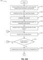
- FIGS. 10A-10F a flowchart 1000 illustrating a method for data transfer on the SoC 102, in accordance with an embodiment of the present invention, is shown.
- the CSI receiver 108 receives the sensor data and the first clock signal from the external camera sensor 104, i.e ., the first DPHY 202 receives the sensor data and the first clock signal.
- the first DPHY 202 generates the active, valid, and sync signals based on the sensor data.
- the first CSI controller 204 generates the data packet based on the sensor data received from the first DPHY 202.
- the first CSI controller 204 performs error correction on the data packet to generate the error signal.
- the first CSI controller 204 separates the packet header and the payload of the data packet and steps 1012 and 1014 are executed.
- the system memory write interface 208 writes the payload into the primary system memory 114.
- the first pipeline controller 212 decodes the type of the data packet based on the packet header.
- the first pipeline controller 212 receives the data packet from the error handler 210.
- the first pipeline controller 212 determines if the data packet is a long packet. If at step 1016, the first pipeline controller 212 determines that the data packet is a long packet, step 1018 is executed.
- the packet header of the data packet is communicated by the CSI receiver 108 to the CSI transmitter 112 over the command FIFO read interface.
- the first pipeline controller 212 writes the packet header of the long data packet into the first buffer 214.
- the first buffer 214 communicates the packet header of the long packet to the header read controller 310 of the CSI transmitter 112.
- the data formatter 216 packs the payload received from the error handler 210 to generate the formatted payload, and steps 1022 and 1024 are executed.
- the data formatter 216 writes the formatted payload into the second buffer 218.
- the formatted payload is written into the loopback buffer 110 by the second buffer 218 and step 1026 is executed.
- the header read controller 310 of the CSI transmitter 112 reads the packet header of the data packet from the first buffer 214.
- the header read controller 310 identifies the size of the payload from the packet header and step 1032 is executed.
- the data formatter 216 determines if the data packet is complete. If at step 1024, the data formatter 216 determines that the data packet is complete, step 1030 is executed. At step 1030, the CSI receiver 108 communicates the EOP signal to the CSI transmitter 112 and step 1032 is executed. However, if at step 1024, the data formatter 216 determines that the data packet is incomplete, step 1020 is executed.
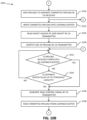
- the CSI transmitter 112 determines if the payload is received completely by the loopback buffer 110. If at step 1032, the CSI transmitter 112 determines that the payload is not received completely by the loopback buffer 110, step 1034 is executed.
- the CSI transmitter 112 determines if the loopback buffer 110 is filled up to the threshold capacity. If at step 1034, the CSI transmitter 112 determines that the loopback buffer 110 is not filled up to the threshold capacity, step 1032 is executed. However, if at step 1034, the loopback buffer 110 determines that the loopback buffer 110 is filled up to the threshold capacity, step 1036 is executed. If at step 1032, the CSI transmitter 112 determines that the payload is received completely by the loopback buffer 110, step 1036 is executed.
- the second pipeline controller 312 of the CSI transmitter 112 generates a read control signal.
- the second pipeline controller 312 receives the packet header of the data packet from the header read controller 310.
- the second pipeline controller 312 identifies the format of the payload and generates the read control signal.
- the data read controller 314 reads the formatted payload from the loopback buffer 110.
- the data read controller 314 further provides the formatted payload to the data un-formatter 316.
- the data un-formatter 316 unpacks the formatted payload to regenerate the payload.
- the data formatter 216 provides the regenerated payload to the second CSI controller 304.
- the second CSI controller 304 combines the packet header and the payload to regenerate the data packet.
- the second CSI controller 304 generates the loopback data based on the data packet and step 1046 is performed.
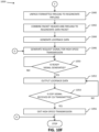
- the second CSI controller 304 generates the request signal for high speed transmission of the loopback data and step 1050 is executed.
- the second CSI controller 304 provides the request signal to the second DPHY 308 for requesting high speed transmission of the loopback data.
- step 1016 if the first pipeline controller 212 determines that the data packet is not a long packet, i.e., the data packet is a short packet, step 1048 is executed.
- step 1048 the first buffer 214 communicates the packet header of the data packet to the header read controller 310 and step 1046 is executed.
- the first buffer 214 receives the packet header of the data packet from the first pipeline controller 212.
- the second CSI controller 304 determines if the ready signal is generated by the second DPHY 308.
- the second DPHY 308 generates the ready signal in response to the request signal. If at step 1050, the second CSI controller 304 determines that the ready signal is generated by the second DPHY 308, step 1052 is executed. However, if at step 1050, the second CSI controller 304 determines that the ready signal is not generated by the second DPHY 308, the second CSI controller 304 waits for the generation of the ready signal.
- the CSI transmitter 112 outputs the loopback data.
- the second CSI controller 304 transmits the loopback data to the second DPHY 308 in response to the ready signal.
- the second DPHY 308 further transmits the loopback data to the processor 106.
- the CSI transmitter 112 determines if it has received the EOP signal from the CSI receiver 108. If at step 1054, the CSI transmitter 112 determines that it has received the EOP signal from the CSI receiver 108, step 1056 is executed. However, if at step 1054, the CSI transmitter 112 determines that it has not received the EOP signal from the CSI receiver 108, step 1052 is executed.
- the second CSI controller 304 exits the high-speed transmission of the loopback data.
- aforementioned method for data transfer on the SoC 102 may be performed for multiple data packets generated by the CSI receiver 108 based on the received sensor data in real-time.
- the multiple data packets are regenerated by the CSI transmitter 112 in real-time.
- the system 100 enables the transfer of the payload in real-time by way of the loopback buffer 110 from the CSI receiver 108 to the CSI transmitter 112.
- the primary system memory 114 is not used for the data transfer between the CSI receiver 108 and the CSI transmitter 112.
- the need to convert the loopback data to a format of the sensor data is eliminated.
- delays in the system 100 are reduced as there is no need to convert the format of the loopback data.
- the system 100 further compensates for frequency offset of the ppm differences between the first and second clock frequencies by transmitting the payload from the CSI receiver 108 to the CSI transmitter 112 through the loopback buffer 110.
- a system and method for real-time data transfer on a system-on-chip allows MIPI-CSI (camera serial interface) data received on a first interface to be output on another MIPI-CSI interface without using system memory or delaying the loopback path.
- the system includes a CSI receiver, a loopback buffer, and a CSI transmitter.
- the loopback buffer is used for the data transfer between the CSI receiver and the CSI transmitter.
- the CSI transmitter receives a payload included in a data packet from the CSI receiver by way of the loopback buffer.
- the CSI receiver communicates a packet header of the data packet to the CSI transmitter.
- the CSI transmitter reads the payload from the loopback buffer based on the packet header and at least one of a buffer threshold capacity and payload size.
Landscapes
- Engineering & Computer Science (AREA)
- Signal Processing (AREA)
- Computer Networks & Wireless Communication (AREA)
- Theoretical Computer Science (AREA)
- Physics & Mathematics (AREA)
- General Physics & Mathematics (AREA)
- Computer Hardware Design (AREA)
- Multimedia (AREA)
- Computer Security & Cryptography (AREA)
- Human Computer Interaction (AREA)
- General Engineering & Computer Science (AREA)
- Communication Control (AREA)
Claims (11)
- System-on-Chip, SoC, (102) mit zwei oder mehr seriellen Hochgeschwindigkeitsschnittstellen, wobei das SoC (102) Folgendes umfasst:einen Empfänger einer seriellen Schnittstelle einer Kamera (108), der ausgelegt ist, Sensordaten über eine erste serielle Schnittstelle zu empfangen und ein Datenpaket zu erzeugen, das eine Nutzlast enthält;einen Loopback-Zwischenspeicher (110), der mit dem CSI-Empfänger (108) verbunden ist, wobei der Zwischenspeicher eine Tiefe besitzt, wobei der CSI-Empfänger (108) ausgelegt ist, die Nutzlast in den Loopback-Zwischenspeicher (110) zu schreiben; undeinen CSI-Sender (112), der zwischen einer zweiten seriellen Schnittstelle und dem Loopback-Zwischenspeicher (110) angeschlossen ist,dadurch gekennzeichnet, dass:das SoC (102) ausgelegt ist, eine Schwellenkapazität des Loopback-Zwischenspeichers anhand der Tiefe des Loopback-Zwischenspeichers zu bestimmen, wobei die Schwellenkapazität ein Punkt ist, bis zu dem der Zwischenspeicher gefüllt werden kann, ohne einen Überlauf zu verursachen;das durch den CSI-Empfänger (108) erzeugte Datenpaket ferner einen Paket-Dateikopf enthält, wobei der Paketdateikopf eine Datenkennung, eine Wortzählung und einen Fehlerkorrekturcode enthält, wobei die Wortzählung eine Größe der Nutzlast spezifiziert;wobei der CSI-Sender (112) konfiguriert ist zum:Empfangen das Paketdateikopfes von dem CSI-Empfänger (108);Identifizieren der Größe der Nutzlast unter Verwendung des Paketdateikopfes;Bestimmen, ob die Größe der Nutzlast, die in dem Loopback-Zwischenspeicher (110) gespeichert ist, gleich der Größe der Nutzlast ist, die aus den Größeninformationen identifiziert wird, durch Vergleichen der identifizierten Größe mit einem Betrag der Nutzlast, die in dem Loopback-Zwischenspeicher (110) gespeichert ist, oder gleich der Schwellenkapazität des Loopback-Zwischenspeichers (110) ist;Lesen der Nutzlast aus dem Loopback-Zwischenspeicher (110), wenn die Schwellenkapazität des Loopback-Zwischenspeichers (110) erreicht ist und/oder die Nutzlast vollständig durch den Loopback-Zwischenspeicher (110) empfangen wurde; undSenden der gelesenen Nutzlast über die zweite serielle Schnittstelle.
- SoC (102) nach Anspruch 1, wobei der CSI-Empfänger (108) Folgendes umfasst:eine erste digitale physikalische Schicht, DPHY, die mit einem externen Kamerasensor durch die erste Schnittstelle zum Empfangen der Sensordaten und eines ersten Taktsignals verbunden ist, wobei die erste DPHY die Sensordaten ausgibt und aktive, synchronisierte und gültige Signale erzeugt, wobei das aktive Signal dann erzeugt wird, wenn die erste DPHY bereit ist, die Sensordaten zu senden, wobei das Synchronisationssignal erzeugt wird, um eine Übertragungsfrequenz der Sensordaten mit einer Frequenz des ersten Taktsignals zu synchronisieren, und das gültige Signal erzeugt wird, wenn die Sensordaten gültig sind;eine erste CSI-Steuereinheit, die mit der ersten DPHY verbunden ist, um die Sensordaten und die aktiven, synchronisierten und gültigen Signale zu empfangen, wobei die erste CSI-Steuereinheit: i) das Datenpaket erzeugt; ii) die Nutzlast und den Paketdateikopf trennt; iii) die Nutzlast und den Paketdateikopf ausgibt; iv) eine Fehlerkorrektur an dem Datenpaket ausführt, um ein Fehlersignal zu erzeugen; und v) ein Signal eines Paketendes, EOP-Signal, erzeugt, wobei das Fehlersignal einen Fehler in dem Datenpaket angibt und das EOP-Signal ein Ende des Datenpakets angibt; undeine erste Loopback-Steuereinheit, die mit der ersten CSI-Steuereinheit verbunden ist, um den Paketdateikopf, die Nutzlast, das EOP-Signal und das Fehlersignal zu empfangen, wobei die erste Loopback-Steuereinheit: i) einen Typ des Datenpakets aus dem Paketdateikopf decodiert; ii) die Nutzlast packt, um eine formatierte Nutzlast zu erzeugen; und iii) den Paketdateikopf und das EOP-Signal an den CSI-Sender kommuniziert, wobei die Nutzlast, die durch den CSI-Empfänger in den Loopback-Zwischenspeicher (110) geschrieben wird, die formatierte Nutzlast ist.
- SoC nach Anspruch 2, wobei die erste Loopback-Steuereinheit umfasst:einen Fehler-Handler, der mit der ersten CSI-Steuereinheit verbunden ist, um den Paketdateikopf, die Nutzlast, das EOP-Signal und das Fehlersignal zu empfangen und den Paketdateikopf, das EOP-Signal und die Nutzlast auszugeben, wobei der Fehler-Handler den Paketdateikopf und die Nutzlast ausgibt, wenn das Fehlersignal angibt, dass das Datenpaket keinen Fehler enthält;eine erste Pipeline-Steuereinheit, die mit dem Fehler-Handler verbunden ist, um den Paketdateikopf und das EOP-Signal zu empfangen, wobei die erste Pipeline-Steuereinheit: i) den Typ des Datenpakets aus dem Paketdateikopf decodiert; ii) den Paketdateikopf und das EOP-Signal ausgibt; und iii) ein Schreibsteuersignal erzeugt, wobei die erste Pipeline-Steuereinheit das EOP-Signal von dem Fehler-Handler empfängt, wenn der Fehler-Handler die gesamte Nutzlast empfängt;einen ersten Zwischenspeicher, der mit der ersten Pipeline-Steuereinheit verbunden ist, um den Paketdateikopf und das EOP-Signal zu empfangen, wobei der erste Zwischenspeicher den Paketdateikopf und das EOP-Signal an den CSI-Sender (112) liefert;einen Datenformatierer, der mit dem Fehler-Handler und der ersten Pipeline-Steuereinheit verbunden ist, um jeweils die Nutzlast und das Schreibsteuersignal zu empfangen, wobei der Datenformatierer die Nutzlast anhand des Schreibsteuersignals packt, um die formatierte Nutzlast zu erzeugen, wenn der Typ des Datenpakets ein langes Paket ist; undeinen zweiten Zwischenspeicher, der mit dem Datenformatierer verbunden ist, um die formatierte Nutzlast zu empfangen, wobei der zweite Zwischenspeicher die formatierte Nutzlast in den Loopback-Zwischenspeicher schreibt.
- SoC nach Anspruch 3, wobei der CSI-Sender (112) Folgendes umfasst:eine zweite Loopback-Steuereinheit, die mit der ersten Loopback-Steuereinheit verbunden ist, um den Paketdateikopf zu lesen und das EOP-Signal zu empfangen, wobei die zweite Loopback-Steuereinheit außerdem mit dem Loopback-Zwischenspeicher verbunden ist, um die formatierte Nutzlast zu empfangen, wobei die zweite Loopback-Steuereinheit: i) die formatierte Nutzlast auspackt, um die Nutzlast zu regenerieren; und ii) den Paketdateikopf ausgibt;eine zweite CSI-Steuereinheit, die mit der zweiten Loopback-Steuereinheit verbunden ist, um den Paketdateikopf und die Nutzlast zu empfangen, wobei die zweite CSI-Steuereinheit den Paketdateikopf und die Nutzlast vereinigt, um das Datenpaket zu regenerieren, und Loopback-Daten und ein Anforderungssignal zum Anfordern einer Hochgeschwindigkeitsübertragung der Loopback-Daten erzeugt, wobei ein Format der Loopback-Daten dasselbe wie ein Format der Sensordaten ist;eine zweite DPHY, die ein zweites Taktsignal empfängt und mit der zweiten CSI-Steuereinheit verbunden ist, um das Anforderungssignal und die Loopback-Daten zu empfangen, wobei die zweite DPHY ein Bereitschaftssignal an die zweite CSI-Steuereinheit sendet und die zweite CSI-Steuereinheit die Loopback-Daten an die zweite DPHY als Reaktion auf das Bereitschaftssignal liefert, und dann die zweite DPHY die Loopback-Daten über die zweite serielle Schnittstelle ausgibt; undeinen Phasenregelkreis, PLL, der mit der zweiten DPHY verbunden ist, um das zweite Taktsignal an die zweite DPHY zu liefern, wobei eine Frequenz des zweiten Taktsignals gleich der Frequenz des ersten Taktsignals ist.
- SoC nach Anspruch 4, wobei die zweite Loopback-Steuereinheit Folgendes umfasst:eine Dateikopflesesteuereinheit, die mit dem ersten Zwischenspeicher verbunden ist, um den Paketdateikopf zu lesen und das EOP-Signal zu empfangen, wobei die Dateikopflesesteuereinheit: i) die Größe der Nutzlast identifiziert; und ii) den Paketdateikopf und Nutzlastgrößeninformationen ausgibt;eine zweite Pipeline-Steuereinheit, die ein Zustandssignal empfängt und mit der Dateikopflesesteuereinheit verbunden ist, um den Paketdateikopf zu empfangen, wobei die zweite Pipeline-Steuereinheit ein Lesesteuersignal erzeugt;eine Datenlesesteuereinheit, die mit der Dateikopflesesteuereinheit, der zweiten Pipeline-Steuereinheit und dem Loopback-Zwischenspeicher verbunden ist, um jeweils die Nutzlastgrößeninformationen, das Lesesteuersignal und die formatierte Nutzlast zu empfangen und die formatierte Nutzlast auszugeben, wobei die Datenlesesteuereinheit die formatierte Nutzlast aus dem Loopback-Zwischenspeicher anhand der Größeninformationen und dem Lesesteuersignal ausliest; undeinen Daten-Unformatierer, der mit der Datenlesesteuereinheit verbunden ist, um die formatierte Nutzlast zu empfangen, wobei der Daten-Unformatierer: i) die formatierte Nutzlast auspackt, um die Nutzlast zu regenerieren; und ii) das Zustandssignal erzeugt, wobei das Zustandssignal einen Zustand des Auspackens der Nutzlast durch den Daten-Unformatierer angibt.
- SoC (102) nach einem der Ansprüche 2 bis 5, das ferner einen primären Systemspeicher umfasst, der mit dem CSI-Empfänger verbunden ist, wobei der CSI-Empfänger die Nutzlast in den primären Systemspeicher schreibt.
- SoC nach Anspruch 6, wobei der CSI-Empfänger ferner eine Systemspeicherschreibschnittstelle umfasst, die mit der ersten CSI-Steuereinheit verbunden ist, um den Paketdateikopf, die Nutzlast, das EOP-Signal und das Fehlersignal zu empfangen, wobei der CSI-Empfänger die Nutzlast in den primären Systemspeicher schreibt.
- Verfahren für eine Datenübertragung in einem System-on-Chip, SoC, (102), das einen Empfänger einer seriellen Schnittstelle einer Kamera, CSI-Empfänger, (108), der mit einer ersten Hochgeschwindigkeitsschnittstelle, HSSI, verbunden ist, einen Loopback-Zwischenspeicher (110) und einem CSI-Sender (122), der mit einer zweiten Hochgeschwindigkeitsschnittstelle, HSSI, verbunden ist, enthält, wobei das Verfahren Folgendes umfasst:Erzeugen durch den CSI-Empfänger (108) eines Datenpakets aus Daten, die über die erste HSSI empfangen werden, wobei das Datenpaket eine Nutzlast und einen Paketdateikopf enthält, wobei der Paketdateikopf eine Datenkennung, eine Wortzählung und einen Fehlerkorrekturcode enthält, wobei die Wortzählung eine Größe der Nutzlast spezifiziert;Schreiben durch den CSI-Empfänger (108) der Nutzlast in den Loopback-Zwischenspeicher;Bestimmen einer Schwellenkapazität des Loopback-Zwischenspeichers (110) anhand der Tiefe des Loopback-Zwischenspeichers, wobei die Schwellenkapazität ein Punkt ist, bis zu dem der Zwischenspeicher gefüllt werden kann, ohne einen Überlauf zu verursachen;Empfangen durch den CSI-Sender (112) des Paketdateikopfes;Identifizieren durch den CSI-Sender (112) der Größe der Nutzlast unter Verwendung des Paketdateikopfes;Bestimmen durch den CSI-Sender (112), ob die Größe der Nutzlast, die in dem Loopback-Zwischenspeicher (110) gespeichert ist, gleich der Größe der Nutzlast ist, die aus den Größeninformationen identifiziert wird, durch Vergleichen der identifizierten Größe mit einem Betrag der Nutzlast, die in dem Loopback-Zwischenspeicher (110) gespeichert ist, oder gleich der Schwellenkapazität des Loopback-Zwischenspeichers (110) ist; undLesen durch den CSI-Sender (112) der Nutzlast aus dem Loopback-Zwischenspeicher, wenn die Schwellenkapazität des Loopback-Zwischenspeichers (110) erreicht ist und/oder die Nutzlast vollständig durch den Loopback-Zwischenspeicher (110) empfangen wurde, und Senden der Nutzlast über die zweite HSSI.
- Verfahren nach Anspruch 8, das ferner Folgendes umfasst:Empfangen durch den CSI-Empfänger (108) von Sensordaten und eines ersten Taktsignals von einem externen Kamerasensor (104) über die erste HSSI;Erzeugen durch den CSI-Empfänger (108) gültiger und synchronisierter Signale, wobei das Synchronisationssignal erzeugt wird, um eine Übertragungsfrequenz der Sensordaten mit einer Frequenz des ersten Taktsignals zu synchronisieren, und das gültige Signal erzeugt wird, wenn die Sensordaten gültig sind;Ausführen durch den CSI-Empfänger (108) einer Fehlerkorrektur an dem Datenpaket;Trennen durch den CSI-Empfänger (108) des Paketdateikopfes und der Nutzlast des Datenpakets;Schreiben durch den CSI-Empfänger (108) der Nutzlast in den Loopback-Zwischenspeicher; undSenden durch den CSI-Empfänger (108) des Paketdateikopfes an den CSI-Sender (112).
- Verfahren nach Anspruch 9, wobei die Schritte des Schreibens der Nutzlast und des Sendens des Paketdateikopfes ferner Folgendes umfassen:Decodieren durch den CSI-Empfänger (108) eines Typs des Datenpakets aus dem Paketdateikopf;Packen durch den CSI-Empfänger (108) der Nutzlast, um eine formatierte Nutzlast zu erzeugen, wenn der Typ des Datenpakets ein langes Paket ist, wobei die durch den CSI-Empfänger (108) in den Loopback-Zwischenspeicher (110) geschriebene Nutzlast die formatierte Nutzlast ist; undKommunizieren durch den CSI-Empfänger (108) eines Signals eines Endes des Pakets, EOP-Signals, an den CSI-Sender (112), wobei das EOP-Signal ein Ende des Datenpakets angibt.
- Verfahren nach Anspruch 10, das ferner Folgendes umfasst:Lesen durch den CSI-Sender (112) der formatierten Nutzlast aus dem Loopback-Zwischenspeicher (110);Regenerieren durch den CSI-Sender (112) der Nutzlast;Vereinigen durch den CSI-Sender (112) der regenerierten Nutzlast und des Paketdateikopfes, um das Datenpaket zu regenerieren;Erzeugen durch den CSI-Sender (112) von Loopback-Daten und eines Anforderungssignals zum Anfordern einer Hochgeschwindigkeitsübertragung der Loopback-Daten, wobei die Loopback-Daten dasselbe Format wie die Sensordaten besitzen;Erzeugen durch den CSI-Sender (112) eines Bereitschaftssignals als Reaktion auf das Anforderungssignal; undAusgeben der Loopback-Daten über die zweite HSSI durch den CSI-Sender (112).
Applications Claiming Priority (1)
| Application Number | Priority Date | Filing Date | Title |
|---|---|---|---|
| US16/222,671 US10862830B2 (en) | 2018-12-17 | 2018-12-17 | Real-time on-chip data transfer system |
Publications (2)
| Publication Number | Publication Date |
|---|---|
| EP3671720A1 EP3671720A1 (de) | 2020-06-24 |
| EP3671720B1 true EP3671720B1 (de) | 2023-08-16 |
Family
ID=68621186
Family Applications (1)
| Application Number | Title | Priority Date | Filing Date |
|---|---|---|---|
| EP19210427.1A Active EP3671720B1 (de) | 2018-12-17 | 2019-11-20 | Echtzeit-on-chip-datenübertragungssystem |
Country Status (2)
| Country | Link |
|---|---|
| US (1) | US10862830B2 (de) |
| EP (1) | EP3671720B1 (de) |
Families Citing this family (4)
| Publication number | Priority date | Publication date | Assignee | Title |
|---|---|---|---|---|
| US20230171374A1 (en) * | 2021-11-29 | 2023-06-01 | Novatek Microelectronics Corp. | Screen control system |
| US11995012B2 (en) | 2022-03-15 | 2024-05-28 | Samsung Electronics Co., Ltd. | High speed interface for multi image sensor device |
| CN115022487B (zh) * | 2022-05-19 | 2025-05-23 | 珠海全志科技股份有限公司 | 高速稳定时间自适应电路及移动产业处理器接口的数据传输方法 |
| US12079071B2 (en) * | 2023-01-12 | 2024-09-03 | Qualcomm Incorporated | Programmable initial packets rejection in a display system interface |
Citations (1)
| Publication number | Priority date | Publication date | Assignee | Title |
|---|---|---|---|---|
| US20090315899A1 (en) * | 2008-06-18 | 2009-12-24 | Ati Technologies Ulc | Graphics multi-media ic and method of its operation |
Family Cites Families (3)
| Publication number | Priority date | Publication date | Assignee | Title |
|---|---|---|---|---|
| US8352793B2 (en) | 2008-08-15 | 2013-01-08 | Apple Inc. | Device testing method and architecture |
| US9977477B2 (en) | 2014-09-26 | 2018-05-22 | Intel Corporation | Adapting operating parameters of an input/output (IO) interface circuit of a processor |
| KR102466160B1 (ko) * | 2016-01-08 | 2022-11-14 | 삼성전자주식회사 | 데이터의 루프백을 수행하는 시스템 온 칩과 집적 회로, 및 이들을 포함하는 모바일 장치 |
-
2018
- 2018-12-17 US US16/222,671 patent/US10862830B2/en not_active Expired - Fee Related
-
2019
- 2019-11-20 EP EP19210427.1A patent/EP3671720B1/de active Active
Patent Citations (1)
| Publication number | Priority date | Publication date | Assignee | Title |
|---|---|---|---|---|
| US20090315899A1 (en) * | 2008-06-18 | 2009-12-24 | Ati Technologies Ulc | Graphics multi-media ic and method of its operation |
Also Published As
| Publication number | Publication date |
|---|---|
| US10862830B2 (en) | 2020-12-08 |
| US20200195589A1 (en) | 2020-06-18 |
| EP3671720A1 (de) | 2020-06-24 |
Similar Documents
| Publication | Publication Date | Title |
|---|---|---|
| EP3671720B1 (de) | Echtzeit-on-chip-datenübertragungssystem | |
| US12362857B2 (en) | Communication device and communication system | |
| US7079528B2 (en) | Data communication method | |
| US7328399B2 (en) | Synchronous serial data communication bus | |
| CN102474438B (zh) | 环状传输系统中的节点装置、集成电路及控制方法 | |
| TWI878595B (zh) | 用於互連協定的錯誤處理的方法以及控制器 | |
| WO2013111010A1 (en) | Chip-to-chip communications | |
| JPS63296540A (ja) | 単一集積回路マイクロ制御器におけるマルチプロトコル通信制御器 | |
| JP2008294757A (ja) | データ伝送装置、データ送信装置、データ受信装置およびデータ伝送システム | |
| EP4170987B1 (de) | Kommunikationsvorrichtung und kommunikationssystem | |
| EP4475476A1 (de) | Kommunikationsvorrichtung und kommunikationssystem | |
| US20230077161A1 (en) | De-skew circuit, de-skew method, and receiver | |
| US6516420B1 (en) | Data synchronizer using a parallel handshaking pipeline wherein validity indicators generate and send acknowledgement signals to a different clock domain | |
| WO2025013918A1 (ja) | 通信装置及び通信システム | |
| US6408012B1 (en) | Signal processing circuit | |
| CN100388776C (zh) | 数字视频储存装置及储存数字视频数据的方法 | |
| CN111970499B (zh) | 一种基于rgif vdma的多路3g-sdi光端机数据解复用方法 | |
| JP2005084792A (ja) | データ通信ユニット | |
| CN114564441B (zh) | 片上系统、数据处理方法及计算机设备 | |
| US20230344552A1 (en) | Communication apparatus, communication system, and communication method | |
| US20220385388A1 (en) | Serial communication apparatus and serial communication method that are capable of efficiently eliminating a timing lag between serial data transferred via a plurality of routes in serial communication | |
| JP2011186791A (ja) | Usbハブ及びusbハブの制御方法 | |
| JP5383147B2 (ja) | 通信制御装置 | |
| KR20250139084A (ko) | Spi를 이용한 통신 방법 및 장치 | |
| JP3941096B2 (ja) | バス・インタフェースにおけるデータ転送方法およびバス・インタフェース |
Legal Events
| Date | Code | Title | Description |
|---|---|---|---|
| PUAI | Public reference made under article 153(3) epc to a published international application that has entered the european phase |
Free format text: ORIGINAL CODE: 0009012 |
|
| STAA | Information on the status of an ep patent application or granted ep patent |
Free format text: STATUS: THE APPLICATION HAS BEEN PUBLISHED |
|
| AK | Designated contracting states |
Kind code of ref document: A1 Designated state(s): AL AT BE BG CH CY CZ DE DK EE ES FI FR GB GR HR HU IE IS IT LI LT LU LV MC MK MT NL NO PL PT RO RS SE SI SK SM TR |
|
| AX | Request for extension of the european patent |
Extension state: BA ME |
|
| STAA | Information on the status of an ep patent application or granted ep patent |
Free format text: STATUS: REQUEST FOR EXAMINATION WAS MADE |
|
| 17P | Request for examination filed |
Effective date: 20210111 |
|
| RBV | Designated contracting states (corrected) |
Designated state(s): AL AT BE BG CH CY CZ DE DK EE ES FI FR GB GR HR HU IE IS IT LI LT LU LV MC MK MT NL NO PL PT RO RS SE SI SK SM TR |
|
| STAA | Information on the status of an ep patent application or granted ep patent |
Free format text: STATUS: EXAMINATION IS IN PROGRESS |
|
| 17Q | First examination report despatched |
Effective date: 20211216 |
|
| GRAP | Despatch of communication of intention to grant a patent |
Free format text: ORIGINAL CODE: EPIDOSNIGR1 |
|
| STAA | Information on the status of an ep patent application or granted ep patent |
Free format text: STATUS: GRANT OF PATENT IS INTENDED |
|
| INTG | Intention to grant announced |
Effective date: 20230517 |
|
| GRAS | Grant fee paid |
Free format text: ORIGINAL CODE: EPIDOSNIGR3 |
|
| GRAA | (expected) grant |
Free format text: ORIGINAL CODE: 0009210 |
|
| STAA | Information on the status of an ep patent application or granted ep patent |
Free format text: STATUS: THE PATENT HAS BEEN GRANTED |
|
| AK | Designated contracting states |
Kind code of ref document: B1 Designated state(s): AL AT BE BG CH CY CZ DE DK EE ES FI FR GB GR HR HU IE IS IT LI LT LU LV MC MK MT NL NO PL PT RO RS SE SI SK SM TR |
|
| REG | Reference to a national code |
Ref country code: CH Ref legal event code: EP |
|
| REG | Reference to a national code |
Ref country code: DE Ref legal event code: R096 Ref document number: 602019035008 Country of ref document: DE |
|
| REG | Reference to a national code |
Ref country code: IE Ref legal event code: FG4D |
|
| P01 | Opt-out of the competence of the unified patent court (upc) registered |
Effective date: 20230907 |
|
| REG | Reference to a national code |
Ref country code: LT Ref legal event code: MG9D |
|
| REG | Reference to a national code |
Ref country code: NL Ref legal event code: MP Effective date: 20230816 |
|
| REG | Reference to a national code |
Ref country code: AT Ref legal event code: MK05 Ref document number: 1600872 Country of ref document: AT Kind code of ref document: T Effective date: 20230816 |
|
| PG25 | Lapsed in a contracting state [announced via postgrant information from national office to epo] |
Ref country code: GR Free format text: LAPSE BECAUSE OF FAILURE TO SUBMIT A TRANSLATION OF THE DESCRIPTION OR TO PAY THE FEE WITHIN THE PRESCRIBED TIME-LIMIT Effective date: 20231117 |
|
| PG25 | Lapsed in a contracting state [announced via postgrant information from national office to epo] |
Ref country code: IS Free format text: LAPSE BECAUSE OF FAILURE TO SUBMIT A TRANSLATION OF THE DESCRIPTION OR TO PAY THE FEE WITHIN THE PRESCRIBED TIME-LIMIT Effective date: 20231216 |
|
| PG25 | Lapsed in a contracting state [announced via postgrant information from national office to epo] |
Ref country code: SE Free format text: LAPSE BECAUSE OF FAILURE TO SUBMIT A TRANSLATION OF THE DESCRIPTION OR TO PAY THE FEE WITHIN THE PRESCRIBED TIME-LIMIT Effective date: 20230816 Ref country code: RS Free format text: LAPSE BECAUSE OF FAILURE TO SUBMIT A TRANSLATION OF THE DESCRIPTION OR TO PAY THE FEE WITHIN THE PRESCRIBED TIME-LIMIT Effective date: 20230816 Ref country code: PT Free format text: LAPSE BECAUSE OF FAILURE TO SUBMIT A TRANSLATION OF THE DESCRIPTION OR TO PAY THE FEE WITHIN THE PRESCRIBED TIME-LIMIT Effective date: 20231218 Ref country code: NO Free format text: LAPSE BECAUSE OF FAILURE TO SUBMIT A TRANSLATION OF THE DESCRIPTION OR TO PAY THE FEE WITHIN THE PRESCRIBED TIME-LIMIT Effective date: 20231116 Ref country code: NL Free format text: LAPSE BECAUSE OF FAILURE TO SUBMIT A TRANSLATION OF THE DESCRIPTION OR TO PAY THE FEE WITHIN THE PRESCRIBED TIME-LIMIT Effective date: 20230816 Ref country code: LV Free format text: LAPSE BECAUSE OF FAILURE TO SUBMIT A TRANSLATION OF THE DESCRIPTION OR TO PAY THE FEE WITHIN THE PRESCRIBED TIME-LIMIT Effective date: 20230816 Ref country code: LT Free format text: LAPSE BECAUSE OF FAILURE TO SUBMIT A TRANSLATION OF THE DESCRIPTION OR TO PAY THE FEE WITHIN THE PRESCRIBED TIME-LIMIT Effective date: 20230816 Ref country code: IS Free format text: LAPSE BECAUSE OF FAILURE TO SUBMIT A TRANSLATION OF THE DESCRIPTION OR TO PAY THE FEE WITHIN THE PRESCRIBED TIME-LIMIT Effective date: 20231216 Ref country code: HR Free format text: LAPSE BECAUSE OF FAILURE TO SUBMIT A TRANSLATION OF THE DESCRIPTION OR TO PAY THE FEE WITHIN THE PRESCRIBED TIME-LIMIT Effective date: 20230816 Ref country code: GR Free format text: LAPSE BECAUSE OF FAILURE TO SUBMIT A TRANSLATION OF THE DESCRIPTION OR TO PAY THE FEE WITHIN THE PRESCRIBED TIME-LIMIT Effective date: 20231117 Ref country code: FI Free format text: LAPSE BECAUSE OF FAILURE TO SUBMIT A TRANSLATION OF THE DESCRIPTION OR TO PAY THE FEE WITHIN THE PRESCRIBED TIME-LIMIT Effective date: 20230816 Ref country code: AT Free format text: LAPSE BECAUSE OF FAILURE TO SUBMIT A TRANSLATION OF THE DESCRIPTION OR TO PAY THE FEE WITHIN THE PRESCRIBED TIME-LIMIT Effective date: 20230816 |
|
| PGFP | Annual fee paid to national office [announced via postgrant information from national office to epo] |
Ref country code: DE Payment date: 20231019 Year of fee payment: 5 |
|
| PG25 | Lapsed in a contracting state [announced via postgrant information from national office to epo] |
Ref country code: PL Free format text: LAPSE BECAUSE OF FAILURE TO SUBMIT A TRANSLATION OF THE DESCRIPTION OR TO PAY THE FEE WITHIN THE PRESCRIBED TIME-LIMIT Effective date: 20230816 |
|
| PG25 | Lapsed in a contracting state [announced via postgrant information from national office to epo] |
Ref country code: ES Free format text: LAPSE BECAUSE OF FAILURE TO SUBMIT A TRANSLATION OF THE DESCRIPTION OR TO PAY THE FEE WITHIN THE PRESCRIBED TIME-LIMIT Effective date: 20230816 |
|
| PG25 | Lapsed in a contracting state [announced via postgrant information from national office to epo] |
Ref country code: SM Free format text: LAPSE BECAUSE OF FAILURE TO SUBMIT A TRANSLATION OF THE DESCRIPTION OR TO PAY THE FEE WITHIN THE PRESCRIBED TIME-LIMIT Effective date: 20230816 Ref country code: RO Free format text: LAPSE BECAUSE OF FAILURE TO SUBMIT A TRANSLATION OF THE DESCRIPTION OR TO PAY THE FEE WITHIN THE PRESCRIBED TIME-LIMIT Effective date: 20230816 Ref country code: ES Free format text: LAPSE BECAUSE OF FAILURE TO SUBMIT A TRANSLATION OF THE DESCRIPTION OR TO PAY THE FEE WITHIN THE PRESCRIBED TIME-LIMIT Effective date: 20230816 Ref country code: EE Free format text: LAPSE BECAUSE OF FAILURE TO SUBMIT A TRANSLATION OF THE DESCRIPTION OR TO PAY THE FEE WITHIN THE PRESCRIBED TIME-LIMIT Effective date: 20230816 Ref country code: DK Free format text: LAPSE BECAUSE OF FAILURE TO SUBMIT A TRANSLATION OF THE DESCRIPTION OR TO PAY THE FEE WITHIN THE PRESCRIBED TIME-LIMIT Effective date: 20230816 Ref country code: CZ Free format text: LAPSE BECAUSE OF FAILURE TO SUBMIT A TRANSLATION OF THE DESCRIPTION OR TO PAY THE FEE WITHIN THE PRESCRIBED TIME-LIMIT Effective date: 20230816 Ref country code: SK Free format text: LAPSE BECAUSE OF FAILURE TO SUBMIT A TRANSLATION OF THE DESCRIPTION OR TO PAY THE FEE WITHIN THE PRESCRIBED TIME-LIMIT Effective date: 20230816 |
|
| REG | Reference to a national code |
Ref country code: DE Ref legal event code: R097 Ref document number: 602019035008 Country of ref document: DE |
|
| PLBE | No opposition filed within time limit |
Free format text: ORIGINAL CODE: 0009261 |
|
| STAA | Information on the status of an ep patent application or granted ep patent |
Free format text: STATUS: NO OPPOSITION FILED WITHIN TIME LIMIT |
|
| REG | Reference to a national code |
Ref country code: CH Ref legal event code: PL |
|
| PG25 | Lapsed in a contracting state [announced via postgrant information from national office to epo] |
Ref country code: MC Free format text: LAPSE BECAUSE OF FAILURE TO SUBMIT A TRANSLATION OF THE DESCRIPTION OR TO PAY THE FEE WITHIN THE PRESCRIBED TIME-LIMIT Effective date: 20230816 |
|
| PG25 | Lapsed in a contracting state [announced via postgrant information from national office to epo] |
Ref country code: LU Free format text: LAPSE BECAUSE OF NON-PAYMENT OF DUE FEES Effective date: 20231120 |
|
| PG25 | Lapsed in a contracting state [announced via postgrant information from national office to epo] |
Ref country code: CH Free format text: LAPSE BECAUSE OF NON-PAYMENT OF DUE FEES Effective date: 20231130 |
|
| 26N | No opposition filed |
Effective date: 20240517 |
|
| GBPC | Gb: european patent ceased through non-payment of renewal fee |
Effective date: 20231120 |
|
| PG25 | Lapsed in a contracting state [announced via postgrant information from national office to epo] |
Ref country code: MC Free format text: LAPSE BECAUSE OF FAILURE TO SUBMIT A TRANSLATION OF THE DESCRIPTION OR TO PAY THE FEE WITHIN THE PRESCRIBED TIME-LIMIT Effective date: 20230816 Ref country code: LU Free format text: LAPSE BECAUSE OF NON-PAYMENT OF DUE FEES Effective date: 20231120 Ref country code: IT Free format text: LAPSE BECAUSE OF FAILURE TO SUBMIT A TRANSLATION OF THE DESCRIPTION OR TO PAY THE FEE WITHIN THE PRESCRIBED TIME-LIMIT Effective date: 20230816 Ref country code: CH Free format text: LAPSE BECAUSE OF NON-PAYMENT OF DUE FEES Effective date: 20231130 Ref country code: SI Free format text: LAPSE BECAUSE OF FAILURE TO SUBMIT A TRANSLATION OF THE DESCRIPTION OR TO PAY THE FEE WITHIN THE PRESCRIBED TIME-LIMIT Effective date: 20230816 |
|
| REG | Reference to a national code |
Ref country code: BE Ref legal event code: MM Effective date: 20231130 |
|
| REG | Reference to a national code |
Ref country code: IE Ref legal event code: MM4A |
|
| PG25 | Lapsed in a contracting state [announced via postgrant information from national office to epo] |
Ref country code: IE Free format text: LAPSE BECAUSE OF NON-PAYMENT OF DUE FEES Effective date: 20231120 |
|
| PG25 | Lapsed in a contracting state [announced via postgrant information from national office to epo] |
Ref country code: GB Free format text: LAPSE BECAUSE OF NON-PAYMENT OF DUE FEES Effective date: 20231120 |
|
| PG25 | Lapsed in a contracting state [announced via postgrant information from national office to epo] |
Ref country code: BE Free format text: LAPSE BECAUSE OF NON-PAYMENT OF DUE FEES Effective date: 20231130 |
|
| PG25 | Lapsed in a contracting state [announced via postgrant information from national office to epo] |
Ref country code: FR Free format text: LAPSE BECAUSE OF NON-PAYMENT OF DUE FEES Effective date: 20231130 |
|
| PG25 | Lapsed in a contracting state [announced via postgrant information from national office to epo] |
Ref country code: IE Free format text: LAPSE BECAUSE OF NON-PAYMENT OF DUE FEES Effective date: 20231120 Ref country code: GB Free format text: LAPSE BECAUSE OF NON-PAYMENT OF DUE FEES Effective date: 20231120 Ref country code: FR Free format text: LAPSE BECAUSE OF NON-PAYMENT OF DUE FEES Effective date: 20231130 Ref country code: BE Free format text: LAPSE BECAUSE OF NON-PAYMENT OF DUE FEES Effective date: 20231130 |
|
| PG25 | Lapsed in a contracting state [announced via postgrant information from national office to epo] |
Ref country code: BG Free format text: LAPSE BECAUSE OF FAILURE TO SUBMIT A TRANSLATION OF THE DESCRIPTION OR TO PAY THE FEE WITHIN THE PRESCRIBED TIME-LIMIT Effective date: 20230816 |
|
| PG25 | Lapsed in a contracting state [announced via postgrant information from national office to epo] |
Ref country code: BG Free format text: LAPSE BECAUSE OF FAILURE TO SUBMIT A TRANSLATION OF THE DESCRIPTION OR TO PAY THE FEE WITHIN THE PRESCRIBED TIME-LIMIT Effective date: 20230816 |
|
| REG | Reference to a national code |
Ref country code: DE Ref legal event code: R119 Ref document number: 602019035008 Country of ref document: DE |
|
| PG25 | Lapsed in a contracting state [announced via postgrant information from national office to epo] |
Ref country code: CY Free format text: LAPSE BECAUSE OF FAILURE TO SUBMIT A TRANSLATION OF THE DESCRIPTION OR TO PAY THE FEE WITHIN THE PRESCRIBED TIME-LIMIT; INVALID AB INITIO Effective date: 20191120 |
|
| PG25 | Lapsed in a contracting state [announced via postgrant information from national office to epo] |
Ref country code: HU Free format text: LAPSE BECAUSE OF FAILURE TO SUBMIT A TRANSLATION OF THE DESCRIPTION OR TO PAY THE FEE WITHIN THE PRESCRIBED TIME-LIMIT; INVALID AB INITIO Effective date: 20191120 |
|
| PG25 | Lapsed in a contracting state [announced via postgrant information from national office to epo] |
Ref country code: DE Free format text: LAPSE BECAUSE OF NON-PAYMENT OF DUE FEES Effective date: 20250603 |
|
| PG25 | Lapsed in a contracting state [announced via postgrant information from national office to epo] |
Ref country code: TR Free format text: LAPSE BECAUSE OF FAILURE TO SUBMIT A TRANSLATION OF THE DESCRIPTION OR TO PAY THE FEE WITHIN THE PRESCRIBED TIME-LIMIT Effective date: 20230816 |