EP3671776A1 - Induktive einheit - Google Patents
Induktive einheit Download PDFInfo
- Publication number
- EP3671776A1 EP3671776A1 EP19217303.7A EP19217303A EP3671776A1 EP 3671776 A1 EP3671776 A1 EP 3671776A1 EP 19217303 A EP19217303 A EP 19217303A EP 3671776 A1 EP3671776 A1 EP 3671776A1
- Authority
- EP
- European Patent Office
- Prior art keywords
- conductive elements
- conductive
- substrate
- assembly according
- inductive
- Prior art date
- Legal status (The legal status is an assumption and is not a legal conclusion. Google has not performed a legal analysis and makes no representation as to the accuracy of the status listed.)
- Withdrawn
Links
- 230000001939 inductive effect Effects 0.000 title claims abstract description 64
- 239000000758 substrate Substances 0.000 claims abstract description 92
- 239000004020 conductor Substances 0.000 claims description 39
- 238000004519 manufacturing process Methods 0.000 claims description 13
- 239000011810 insulating material Substances 0.000 claims description 5
- 229910000679 solder Inorganic materials 0.000 claims description 3
- 238000004804 winding Methods 0.000 description 14
- 238000000034 method Methods 0.000 description 6
- 239000000463 material Substances 0.000 description 5
- RYGMFSIKBFXOCR-UHFFFAOYSA-N Copper Chemical compound [Cu] RYGMFSIKBFXOCR-UHFFFAOYSA-N 0.000 description 4
- 229910052802 copper Inorganic materials 0.000 description 4
- 239000010949 copper Substances 0.000 description 4
- 238000005520 cutting process Methods 0.000 description 4
- 230000001965 increasing effect Effects 0.000 description 4
- 238000005476 soldering Methods 0.000 description 4
- 238000003780 insertion Methods 0.000 description 3
- 230000037431 insertion Effects 0.000 description 3
- 238000004377 microelectronic Methods 0.000 description 3
- XECAHXYUAAWDEL-UHFFFAOYSA-N acrylonitrile butadiene styrene Chemical compound C=CC=C.C=CC#N.C=CC1=CC=CC=C1 XECAHXYUAAWDEL-UHFFFAOYSA-N 0.000 description 2
- 229920000122 acrylonitrile butadiene styrene Polymers 0.000 description 2
- 239000004676 acrylonitrile butadiene styrene Substances 0.000 description 2
- 238000005219 brazing Methods 0.000 description 2
- 230000002500 effect on skin Effects 0.000 description 2
- 230000000694 effects Effects 0.000 description 2
- 239000012777 electrically insulating material Substances 0.000 description 2
- 230000004907 flux Effects 0.000 description 2
- 239000004593 Epoxy Substances 0.000 description 1
- 238000000151 deposition Methods 0.000 description 1
- 239000003822 epoxy resin Substances 0.000 description 1
- 238000005530 etching Methods 0.000 description 1
- 230000003100 immobilizing effect Effects 0.000 description 1
- 230000010354 integration Effects 0.000 description 1
- 239000000696 magnetic material Substances 0.000 description 1
- 239000002184 metal Substances 0.000 description 1
- 229910052751 metal Inorganic materials 0.000 description 1
- 239000004033 plastic Substances 0.000 description 1
- 229920003023 plastic Polymers 0.000 description 1
- 229920000647 polyepoxide Polymers 0.000 description 1
- 229920001296 polysiloxane Polymers 0.000 description 1
- XLYOFNOQVPJJNP-UHFFFAOYSA-N water Substances O XLYOFNOQVPJJNP-UHFFFAOYSA-N 0.000 description 1
Images


Classifications
-
- H—ELECTRICITY
- H01—ELECTRIC ELEMENTS
- H01F—MAGNETS; INDUCTANCES; TRANSFORMERS; SELECTION OF MATERIALS FOR THEIR MAGNETIC PROPERTIES
- H01F27/00—Details of transformers or inductances, in general
- H01F27/28—Coils; Windings; Conductive connections
- H01F27/2847—Sheets; Strips
-
- H—ELECTRICITY
- H01—ELECTRIC ELEMENTS
- H01F—MAGNETS; INDUCTANCES; TRANSFORMERS; SELECTION OF MATERIALS FOR THEIR MAGNETIC PROPERTIES
- H01F27/00—Details of transformers or inductances, in general
- H01F27/28—Coils; Windings; Conductive connections
- H01F27/2895—Windings disposed upon ring cores
-
- H—ELECTRICITY
- H01—ELECTRIC ELEMENTS
- H01F—MAGNETS; INDUCTANCES; TRANSFORMERS; SELECTION OF MATERIALS FOR THEIR MAGNETIC PROPERTIES
- H01F27/00—Details of transformers or inductances, in general
- H01F27/02—Casings
- H01F27/022—Encapsulation
-
- H—ELECTRICITY
- H01—ELECTRIC ELEMENTS
- H01F—MAGNETS; INDUCTANCES; TRANSFORMERS; SELECTION OF MATERIALS FOR THEIR MAGNETIC PROPERTIES
- H01F27/00—Details of transformers or inductances, in general
- H01F27/28—Coils; Windings; Conductive connections
- H01F27/32—Insulating of coils, windings, or parts thereof
Definitions
- the present invention relates to an inductive assembly and to its production method.
- Inductive devices are for example used in very high frequency converters and switching power supplies for power electronics and in high frequency transformers.
- An inductive device is a device comprising an electric circuit forming a winding so that, when an electric current flows in the electric circuit, a magnetic flux appears inside the winding.
- the inductive device may include a core disposed in an area where the winding creates the magnetic flux.
- Inductive devices or coils are generally produced by winding a wire conductor around a core.
- Windings with flat conductors i.e. having a small thickness compared to their width can then be used to mitigate the appearance of this phenomenon.
- One solution is to carry out such a winding with the techniques of microelectronics, ie by implementing layers, in which the conductors are produced by conductive tracks in different planes and are connected between them by via.
- the conductors are produced by conductive tracks in different planes and are connected between them by via.
- the document US 9754714 describes an embodiment of an inductive device comprising flat conductors.
- the device comprises a first substrate provided with a face in which an annular recess is formed in which the first flat conductive elements are arranged flat next to each other, each first flat conductive element is arranged on the two annular edges and the bottom of the recess and has two tabs at each of its ends flat on the face of the first substrate.
- the device comprises a second substrate comprising second electrical conductors arranged so as to form, with the first conductive elements, windings.
- a core is disposed in the annular recess inside the first conductive elements.
- an inductive device comprising at least a first conductive element and a substrate with at least a second conductive element.
- the at least first conductive element extends in at least one plane different from the substrate, said at least one first conductive element being electrically connected to at least one second conductive element, said at least one first conductive element being configured so that its grip the ground is reduced compared to the devices of the prior art.
- the first conductive element comprises two large surface areas separated by a small thickness and forming a conductive path comprising first and second portions each connected to a second conductive element and a third connection portion between the first and second portions, the third portion being oriented so that the current lines are at different distances from the substrate by considering a transverse direction of the faces with respect to the flow of current.
- the first conductive element or elements have a shape such that, while having the same current flow section, their projection onto the substrate is substantially reduced.
- the number of first conductive elements which can be mounted on the substrate is increased, as well as the number of turns formed.
- the device according to the invention is of easier manufacture compared to the inductive devices of the state of the art, in particular those having a closed contour, such as toric-shaped devices.
- the first conductive elements extend mainly transversely relative to the substrate, which significantly reduces the footprint of each first conductive element.
- the number of windings achievable is significantly increased.
- Part of the inductive circuit is made in the substrate and another part is made above the substrate and can implement several electrical conductors above the substrate arranged side by side.
- the first conductive elements are planar and are orthogonal to the substrate, their projection is reduced to the thickness of the first conductive element
- the first conductive elements have U-shapes, the free ends of the U being connected to the second conductors.
- the first conductive elements can be cut from metal plates, for example from copper plates, or be produced separately in the form of a printed circuit, for example by depositing at least one conductive line on an insulating substrate , for example in epoxy.
- the present invention is particularly advantageous for producing inductive devices with closed contours, such as toric devices which are very difficult to produce by conventional winding techniques.
- the current The invention is also very advantageous for producing inductive devices of the EI type, since it avoids using a multi-part core in which the presence of an air gap cannot be avoided.
- the present invention also makes it easy to carry out several windings simultaneously, for example for producing a current or voltage transformer.
- first conductive elements are connected to the substrate on the two faces of the substrate each comprising second conductive elements.
- the present invention has the advantage of making it possible to produce inductive devices on printed circuit boards which can integrate other functions.
- the invention achieves a high level of integration.
- the present invention therefore relates to an inductive assembly comprising at least n first conductive elements and a substrate comprising at least n second conductive elements, n being an integer greater than or equal to 1, each first conductive element extending at least partly in a plane different from the substrate, and comprising a first end and a second end connected by an electrically conductive path, the conductive path comprising a first portion electrically connected to one of the second conductive elements by the first end, and a second portion electrically connected to the other of said second conductive elements by the second end, and at least a third connection portion between the first portion and the second portion, the conductive path also comprising two faces connected by edges, said faces having a very large surface relative to that of the edges so that the conductive path has a e small thickness, the faces having a transverse dimension relative to the direction of circulation of the electric current in said conductive path.
- the first, second and third portions are oriented so that the current lines flowing in the third portion are located at different distances from the substrate in the transverse direction of
- n is greater than or equal to 2
- a first portion of an electrically conductive element is electrically connected to one of the second conductive elements through the first end, and a second portion of the electrically conductive element is electrically connected to the other of said second conductive elements by the second end.
- the transverse dimension is substantially constant along the conductive path between the first end and the second end.
- each first conducting element is contained in one or more planes, each plane being orthogonal to the substrate.
- each first conductive element is contained entirely in a plane distinct from the planes containing the other first conductive elements.
- the first n conductive elements and the second second conductive elements are electrically connected forming a single inductive device.
- At least a first part of the first conductive elements and second conductive elements are electrically connected to each other and a second part of the first conductive elements and second conductive elements are electrically connected to each other and electrically isolated from the first part of the first elements conductors and second conductive elements, forming two inductive devices.
- the first conducting elements have the shape of a U, the first and second portions forming the branches of the U and the third portion forms the bottom of the U.
- the first and second ends may include at least one mechanical and / or electrical connection tab.
- the substrate has holes in which the connection tabs are inserted.
- connection tab can be held in an orifice by mechanical cooperation with the wall of the orifice and / or by a solder.
- the assembly includes first conductive elements on one face of the substrate and first conductive elements on the other face of the substrate.
- first n conductive elements and the second second conductive elements are distributed radially so as to form one or more toroidal inductive devices.
- the second conductive elements can be distributed in several substantially parallel planes of the substrate.
- each first conductive element is cut from a plate of electrically conductive material.
- each first conductive element comprises a substrate made of electrically insulating material and a track made of electrically conductive material between the first and the second end and forming the conductive path.
- the substrate is advantageously a printed circuit.
- the first conductive elements are held integral with each other by an overmolded electrical insulating material.
- the present invention also relates to an electrical transformer comprising at least one inductive assembly according to the invention.
- the first part of the first conductive elements and second conductive elements form a primary and the second part of the first conductive elements and second conductive elements form a secondary.
- the first n conductive elements can be manufactured by cutting a plate of electrically conductive material, or the first n conductive elements are manufactured from a printed circuit.
- connection tabs of the first conductive elements are, for example, inserted into holes in the substrate.
- the mechanical fixing and the electrical connection are made by soldering the connection lugs of the first conductive elements to and / or in the second conductive elements and / or by inserting the lugs of the orifices of the substrate.
- the first n conductive elements Prior to mounting, the first n conductive elements can be fixed relative to each other and then be simultaneously mounted on the substrate.
- the first n conductive elements are mounted in a tool.
- an electrical insulating material is overmolded on the first conductive elements and are held stationary with respect to each other.
- conductor means “electrical conductor”.
- the term "substrate” means a planar or substantially planar element comprising a part made of electrically insulating material and several conductive tracks which extend at least in the plane of the substrate.
- the substrate can include conductive tracks in several levels of the substrate, preferably parallel to each other and which can be connected by vias.
- a substrate is manufactured by microelectronic techniques.
- a printed circuit or PCB (Printed Circuit Board in English terminology) is an example of a substrate according to the invention.
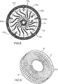
- an inductive device comprising a substrate 2, a plurality of first electrical conductive elements E1 and a core 4 disposed in the space delimited by the substrate 2 and the first conductive elements E1 .
- the substrate extends in the XY plane and the first conductive elements E1 extend in planes orthogonal to the XY plane and containing the direction Z.
- the substrate 2 has the shape of a disc and the core 4 has the shape of a ring with an outside diameter smaller than the diameter of the substrate, so as to provide an outer annular flange on the substrate to fix a free end of the first conductive elements E1.
- the first conductive elements E1 are fixed on the substrate 2 which forms both a mechanical support and an electrical connector.
- the first conductive element E1 represented alone.
- the first conductive element E1 is contained in a plane and has a U shape, the two free ends E1.1, E1.2 of which are intended to be fixed to the substrate 6.
- the branches are designated by B1, B2 and the bottom 15 of the U connecting the two branches.
- the first conductive element comprises a conductive path CC connecting the two ends E1.1 and E1.2.
- the conductive path CC has a transverse dimension L which is perpendicular to the direction of current flow symbolized by the current lines I1, I2, I3 on the figure 5 .
- the transverse dimension L is substantially constant along the conductive path between the first and the second end.
- the conductive path CC of each first conductive element E1 and the conductive path of each second conductive element E2 have current passage sections close to or equal.
- the conductive path CC comprising two large faces F connected by two flanges R.
- the two faces are separated by a small distance e from the other dimensions of the first conductive element and which corresponds to the thickness of the conductive path .
- the first conductive element E1 has a height h.
- the two branches B1 and B2 of the U have the same height h.
- the bottom of the U or connection portion 15 has a dimension I between the two branches B2, B2.
- e / L Preferably e / L ⁇ 1. Also preferably, L> 0.5 mm, I> 1 mm and 10 ⁇ m ⁇ e ⁇ 0.5 mm.
- connection bridges For simplicity, the first conductive elements E1 will be designated “connection bridges" in the following description.
- the E1 connection bridge of the figure 2A is made entirely of electrically conductive material, for example by cutting from a sheet of conductive material, for example copper. Thus the conductive path forms the connection bridge.
- the thickness of the plate of electrically conductive material is sufficient for the first conductive elements to be self-supporting.
- the free ends E1.1 and E1.2 each comprise two conductive tabs 6 which are intended to connect the first conductive element E1 to second conductors E2 formed in, or on, the substrate 2. It will be understood that the number of legs 6 is not limiting.
- the substrate has orifices O for the insertion of the tabs 6 of the first conductive elements.
- the orifices O have shapes adapted to the shape of the legs, they are for example circular for cylindrical legs with circular section or oblong for legs in the form of a blade.
- the first conductive elements can be secured to the substrate for example by soldering or by insertion, preferably cold.
- the mechanical connection and the electrical connection can be made by the same or different means.
- the second electrical conductors E2 formed by conductive tracks located on at least one face of the substrate 2.
- the second conductors E2 extend substantially radially on the substrate 2, so that a free end of a connection bridge E1 located radially outside, and the free end of another adjacent connection bridge E1 located radially inside can connect to the same second conductor E2 and thus form a winding.
- a free end of a first conductive element E1 is electrically connected to a second conductive element E2, which is distinct from that to which the other free end of the same first conductive element is connected, so as to electrically connect all the first conductive elements in series and to form with the second conductors of the windings.
- E1 and E1 ' denote two first directly adjacent conductive elements, a free end E1.1 of the first conductive element E1 located radially on the outside is electrically connected to the second conductor E2, a free end E1.1' of the first conductive element E1 ' located radially inside is electrically connected to the second conductor E2.
- the current lines I1, I2, I3 are shown on the figure 5 . We can see that the current line I1 is closer to the substrate than the lines I2 and I3.
- the first conductive elements E1 are for example produced by cutting from a plate of electrically conductive material, for example a copper plate. For example, it is a LASER cut, water jet cut ..., a stamping, a knife roller cut.
- each first conductive element is located in a plane.
- the plane of each conductor is perpendicular to the plane of the substrate.
- the first conductive elements are arranged radially with respect to each other.
- the configuration and orientation of the connection bridges which preferably extend in planes transverse to the substrate, makes it possible to substantially reduce the size of each bridge in the plane of the substrate.
- the radially inner ends of the second conductive elements are on the same circle, and the radially inner ends of the second conductive elements are on the same circle.
- the same first elements can be used for all the turns.
- a toroidal inductive device is thus formed.
- connection bridge forms part of a turn and each second conductive element forms another part of the turn, the proportions of the turn formed by the connection bridge and by the second conductive element are variable, preferably the proportions are 3 / 4 and 1/4 respectively.
- connection ends comprise a tab 6.
- This variant is advantageous in the device of the figure 1 because the tab of the end connecting to the central part of the substrate is located on a larger diameter, which allows more space for the connection between the connection end and the second conductor radially inside .
- each end has a tab 6 whose width represents only part of the width of the conductive path, for example half in the example shown.
- the tabs are located on the same side of the conductive path and the first conductive element is oriented so that the tabs are located radially on the outside.
- This variant is even more advantageous, because it ensures a sufficient current flow section while ensuring a connection to a larger diameter.
- the legs are located in the center of the conductive path.
- connection bridges and the second conductive elements are carried out by inserting the tabs into the orifices made in the substrate and by possible soldering.
- connection bridge comprises two connection tabs 16 intended to come into plane support against the second connection elements and to be secured thereto, for example by soldering.
- brazing paste 18 is interposed between each connection tab 16 and the second connection element E2.
- each first conductive element may be envisaged to overmold with an electrical insulating material except at the level of the electrical contacts.
- the first conductive element in the form of a printed circuit. It comprises an electrical insulating support 10 on and / or in which a conductive track 12 is formed, forming the conductive path. Connection tabs 14 to the substrate are formed.
- several tracks can be formed on one face of the printed circuit.
- one or more electrical tracks can be produced on the two faces of the printed circuit, thus at least two portions of turns can be formed on the same printed circuit.
- connection bridges are contained in a plane.
- connection bridges are contained in several plans.
- the branches B1 and B2 are contained in intersecting planes.
- connection bridges can be waved looking in the direction of the Z axis.
- connection portion 15 which is contained in a plane distinct from the branches.
- connection portion 15 which is contained in a plane distinct from the branches.
- FIG 7B we can see several bridges of the figure 7A , seen from the side, arranged side by side, illustrating the fact that they make it possible to produce an inductive device having a high density of turns.
- connection bridges Figures 6A to 7B are arranged relative to each other so as to fit together.
- the shape in several planes nevertheless makes it possible to obtain a high density of turns.
- the shape of the first conductive elements can have other shapes than a U shape, for example a V shape.
- connection portion 15 the plane or planes containing the connection portion 15 are not parallel to the substrate in order to reduce the footprint of the connection bridges
- the first conductive elements are mounted one by one on the substrate and electrically connected to the second conductive elements.
- connection bridges are arranged in a holding tool which simultaneously mounts all the connection bridges on the substrate.
- the device of the figure 9 comprises an overmolding 20 is produced on the first conductive elements E1 forming a one-piece assembly, immobilizing the first conductive elements with respect to each other before mounting on the substrate and facilitating the assembly of the first conductive elements on the substrate 2.
- the overmolded material is electrically insulating and provides protection.
- the overmolded material can advantageously participate at least in the mechanical connection of the first electrical conductive elements with the substrate 2.
- the overmolded material is example a plastic material, for example ABS (acrylonitrile butadiene styrene), an epoxy resin, a silicone material
- the distance d between two radially inner ends of the first two conductive elements can be of the order of 1 mm ben the absence of overmolding (FIG. 1).
- the distance d can be of the order of 0.3 mm ( figure 9 ).
- the first conductive elements and their relative arrangement are identical to those of the device of the figure 1 .
- the substrate includes groups of second electrical conductors.
- a first group of second electrical conductors participates in the electrical connection of first conductive elements E1 to each other to form the primary and a second group participates in the electrical connection of other first electrical conductive elements E1 to each other to form the secondary.
- the references E2p designate the electrical conductors ensuring the connections between the first conductive elements E1 to form the primary and the references E2s designate the electrical conductors ensuring the connections between the first conductive elements E1 to form the secondary.
- the radially outer ends of the second electrical connector elements E2p and E2s of the two groups are located on the same circle C1 and the radially inner ends of the second electrical connectors E2p and E2s of the two groups are located on the same circle C2.
- the two inductive devices are produced with connection bridges of different geometries, the connections to the second conductors being located on different circles.
- the second conductors E2p and the second conductors E2s are produced in separate planes.
- connection bridges are located on one side of the substrate.
- connection bridges are located on both sides of the substrate. It can then be envisaged to produce separate inductive devices on each of the faces and / or to produce one or more separate inductive devices on the two faces, each turn of a device being formed by a connection bridge on one side and a bridge. connection on the other side.
- the inductive device or devices may or may not comprise cores of magnetic material. In the case where separate inductive devices are produced on the two faces of the substrate, one may have a core and the other may not have one.
- the first conductive elements are produced by cutting from a copper plate.
- the first conductive elements are for example those of the figure 2A .
- the substrate provided with second conductive elements is manufactured by microelectronic techniques, for example by etching a printed circuit. Holes are made through the substrate at the inner and outer radial ends of the second conductive elements for the insertion of the electrical contacts of the first conductive elements.
- the core is placed on the substrate.
- the electrical contacts 6 of the first conductive elements E1 are inserted into the holes and overlap the core.
- all the first elements are mounted in a tool to ensure simultaneous mounting of all the first conductive elements on the substrate. Brazing can be performed if this is required at each electrical contact in order to electrically connect each electrical contact to a second conductive element.
- the inductive device is finished.
- the method according to the invention is particularly advantageous for manufacturing inductive devices with a closed contour, such as toric or E inductive devices.
- a closed contour such as toric or E inductive devices.
- the present invention applies to inductive devices of any shape, for example to an inductive device in the form of a bar.
- the invention is also very advantageous for producing several inductive devices simultaneously and having a reduced bulk.
- the inductive device according to the invention can very advantageously allow the winding of the inductor of electric motors.
- the invention also has the advantage of making it possible to integrate one or more inductive devices directly on a substrate comprising other electronic functions, for example the rectifying circuit of a transformer of an electronic power system.
- the diodes can be soldered to the substrate directly at the ends of the connection bridges providing the secondary of the transformer.
Landscapes
- Engineering & Computer Science (AREA)
- Power Engineering (AREA)
- Coils Or Transformers For Communication (AREA)
- Combinations Of Printed Boards (AREA)
Applications Claiming Priority (1)
| Application Number | Priority Date | Filing Date | Title |
|---|---|---|---|
| FR1873423A FR3090991A1 (fr) | 2018-12-19 | 2018-12-19 | Ensemble inductif |
Publications (1)
| Publication Number | Publication Date |
|---|---|
| EP3671776A1 true EP3671776A1 (de) | 2020-06-24 |
Family
ID=66530270
Family Applications (1)
| Application Number | Title | Priority Date | Filing Date |
|---|---|---|---|
| EP19217303.7A Withdrawn EP3671776A1 (de) | 2018-12-19 | 2019-12-18 | Induktive einheit |
Country Status (2)
| Country | Link |
|---|---|
| EP (1) | EP3671776A1 (de) |
| FR (1) | FR3090991A1 (de) |
Cited By (1)
| Publication number | Priority date | Publication date | Assignee | Title |
|---|---|---|---|---|
| WO2024072933A1 (en) * | 2022-09-29 | 2024-04-04 | Tesla, Inc. | Orthogonal joined plate windings for toroidal magnetics |
Citations (6)
| Publication number | Priority date | Publication date | Assignee | Title |
|---|---|---|---|---|
| DE29511040U1 (de) * | 1995-07-07 | 1995-09-14 | Theo Benning Elektrotechnik und Elektronik GmbH & Co. KG, 46397 Bocholt | Drossel mit Kern für hohe Ströme |
| JP2003309012A (ja) * | 2002-04-12 | 2003-10-31 | Toshiba Corp | 表面実装用磁性部品とそれを用いた表面実装回路装置 |
| FR2874123A1 (fr) * | 2004-08-03 | 2006-02-10 | Peugeot Citroen Automobiles Sa | Procede pour la realisation d'une bobine d'inductance a noyau magnetique torique sur une plaquette de circuit imprime et bobine realise selon ce procede |
| WO2006053862A1 (de) * | 2004-11-19 | 2006-05-26 | SIEMENS AKTIENGESELLSCHAFT öSTERREICH | Induktives schaltungselement und verfahren zur montage eines induktiven schaltungselements |
| DE102014005118A1 (de) * | 2014-04-08 | 2015-10-08 | Rosenberger Hochfrequenztechnik Gmbh & Co. Kg | Entstördrossel |
| US9754714B2 (en) | 2009-07-31 | 2017-09-05 | Radial Electronics, Inc. | Embedded magnetic components and methods |
-
2018
- 2018-12-19 FR FR1873423A patent/FR3090991A1/fr not_active Withdrawn
-
2019
- 2019-12-18 EP EP19217303.7A patent/EP3671776A1/de not_active Withdrawn
Patent Citations (6)
| Publication number | Priority date | Publication date | Assignee | Title |
|---|---|---|---|---|
| DE29511040U1 (de) * | 1995-07-07 | 1995-09-14 | Theo Benning Elektrotechnik und Elektronik GmbH & Co. KG, 46397 Bocholt | Drossel mit Kern für hohe Ströme |
| JP2003309012A (ja) * | 2002-04-12 | 2003-10-31 | Toshiba Corp | 表面実装用磁性部品とそれを用いた表面実装回路装置 |
| FR2874123A1 (fr) * | 2004-08-03 | 2006-02-10 | Peugeot Citroen Automobiles Sa | Procede pour la realisation d'une bobine d'inductance a noyau magnetique torique sur une plaquette de circuit imprime et bobine realise selon ce procede |
| WO2006053862A1 (de) * | 2004-11-19 | 2006-05-26 | SIEMENS AKTIENGESELLSCHAFT öSTERREICH | Induktives schaltungselement und verfahren zur montage eines induktiven schaltungselements |
| US9754714B2 (en) | 2009-07-31 | 2017-09-05 | Radial Electronics, Inc. | Embedded magnetic components and methods |
| DE102014005118A1 (de) * | 2014-04-08 | 2015-10-08 | Rosenberger Hochfrequenztechnik Gmbh & Co. Kg | Entstördrossel |
Cited By (1)
| Publication number | Priority date | Publication date | Assignee | Title |
|---|---|---|---|---|
| WO2024072933A1 (en) * | 2022-09-29 | 2024-04-04 | Tesla, Inc. | Orthogonal joined plate windings for toroidal magnetics |
Also Published As
| Publication number | Publication date |
|---|---|
| FR3090991A1 (fr) | 2020-06-26 |
Similar Documents
| Publication | Publication Date | Title |
|---|---|---|
| FR2601218A1 (fr) | Transformateur a tore carre pour circuit integre hybride | |
| EP2912725B1 (de) | Elektrischer kontakt und elektronische schaltung | |
| EP1157395B1 (de) | Induktives elektronisches bauteil, und herstellungsverfahren | |
| FR3071112A1 (fr) | Systeme de connexion pour machine electrique. | |
| EP2401786A1 (de) | Mechanische und elektrische verbindungsvorrichtung für ein koaxialkabel zur übermittlung eines hochfrequenzsignals | |
| EP3176919B1 (de) | Elektrischer steckverbinder zur elektrischen verbindung mit einer stromquelle | |
| EP3671776A1 (de) | Induktive einheit | |
| TW201334125A (zh) | 表面黏著式電子組件 | |
| FR2993397A1 (fr) | Dispositif semi-conducteur comprenant un condensateur integre et procede de fabrication | |
| EP3387737B1 (de) | Elektromotor | |
| EP0065910A1 (de) | Magnetischer Kreis, Drossel mit derartigem magnetischem Kreis und Verfahren zur Herstellung von Drosseln | |
| EP3072372B1 (de) | Elektronische karte mit magnetischen elementen | |
| EP2879234B1 (de) | Elektronisches Gerät mit in einem Gehäuse zusammengefalteter Funkantenne | |
| FR2721431A1 (fr) | Procédé pour réaliser des composants magnétiques à bobinages simplifiés, et composants ainsi réalisés. | |
| EP3633700A1 (de) | Transformationsvorrichtung, die einen transformator und elektrische komponenten umfasst | |
| FR3084530A1 (fr) | Structure de broche accommodante pour des composants électriques discrets | |
| FR3060901B1 (fr) | Module electronique de puissance | |
| EP3721501A1 (de) | Mikrowellen-bauelement und zugehöriges herstellungsverfahren | |
| FR3103625A1 (fr) | Bobinage, procédé de réalisation correspondant et aéronef comportant un tel bobinage | |
| FR2742589A1 (fr) | Module de connecteur electrique a haute densite et procede de montage de contacts et de capots dans un tel module | |
| EP0023165B1 (de) | Tragplatte für Leitergitter, insbesondere für integriertes Schaltungsgehäuse, und Gehäuse mit solcher Tragplatte | |
| WO2021224559A2 (fr) | Transformateur planaire équipé de composants, carte mère comprenant un tel transformateur planaire et procédé d'assemblage d'une telle carte mère. | |
| FR3073085B1 (fr) | Ensemble guide d'onde et procede d'assemblage associe | |
| EP2134147A2 (de) | Verfahren zum Auflöten und Positionieren einer integrierten Schaltung auf ein Substrat und mit diesem Verfahren hergestellte Anordnung | |
| FR2641438A1 (fr) | Circuit inductif integre |
Legal Events
| Date | Code | Title | Description |
|---|---|---|---|
| PUAI | Public reference made under article 153(3) epc to a published international application that has entered the european phase |
Free format text: ORIGINAL CODE: 0009012 |
|
| STAA | Information on the status of an ep patent application or granted ep patent |
Free format text: STATUS: REQUEST FOR EXAMINATION WAS MADE |
|
| 17P | Request for examination filed |
Effective date: 20191218 |
|
| AK | Designated contracting states |
Kind code of ref document: A1 Designated state(s): AL AT BE BG CH CY CZ DE DK EE ES FI FR GB GR HR HU IE IS IT LI LT LU LV MC MK MT NL NO PL PT RO RS SE SI SK SM TR |
|
| AX | Request for extension of the european patent |
Extension state: BA ME |
|
| STAA | Information on the status of an ep patent application or granted ep patent |
Free format text: STATUS: THE APPLICATION IS DEEMED TO BE WITHDRAWN |
|
| 18D | Application deemed to be withdrawn |
Effective date: 20210112 |