EP3671797A1 - Dispositif de commutation de sécurité - Google Patents
Dispositif de commutation de sécurité Download PDFInfo
- Publication number
- EP3671797A1 EP3671797A1 EP18213553.3A EP18213553A EP3671797A1 EP 3671797 A1 EP3671797 A1 EP 3671797A1 EP 18213553 A EP18213553 A EP 18213553A EP 3671797 A1 EP3671797 A1 EP 3671797A1
- Authority
- EP
- European Patent Office
- Prior art keywords
- antenna
- switching
- switching device
- safety
- switching element
- Prior art date
- Legal status (The legal status is an assumption and is not a legal conclusion. Google has not performed a legal analysis and makes no representation as to the accuracy of the status listed.)
- Granted
Links
Images


Classifications
-
- H—ELECTRICITY
- H01—ELECTRIC ELEMENTS
- H01H—ELECTRIC SWITCHES; RELAYS; SELECTORS; EMERGENCY PROTECTIVE DEVICES
- H01H47/00—Circuit arrangements not adapted to a particular application of the relay and designed to obtain desired operating characteristics or to provide energising current
- H01H47/002—Monitoring or fail-safe circuits
-
- H—ELECTRICITY
- H01—ELECTRIC ELEMENTS
- H01H—ELECTRIC SWITCHES; RELAYS; SELECTORS; EMERGENCY PROTECTIVE DEVICES
- H01H9/00—Details of switching devices, not covered by groups H01H1/00 - H01H7/00
- H01H9/16—Indicators for switching condition, e.g. "on" or "off"
- H01H9/167—Circuits for remote indication
-
- H—ELECTRICITY
- H01—ELECTRIC ELEMENTS
- H01H—ELECTRIC SWITCHES; RELAYS; SELECTORS; EMERGENCY PROTECTIVE DEVICES
- H01H9/00—Details of switching devices, not covered by groups H01H1/00 - H01H7/00
- H01H9/16—Indicators for switching condition, e.g. "on" or "off"
- H01H9/168—Indicators for switching condition, e.g. "on" or "off" making use of an electromagnetic wave communication
Definitions
- the present invention relates to a safety switching device for switching an electrical consumer that can be connected to the switching device, in particular an electrical machine.
- the invention is therefore based on the knowledge that the actual switching state of the switching element can be determined by radio transmission of the test signal if the actual switching state has an influence on the test signal. In this way, the actual switching state can be reliably determined using an arrangement of two antennas that is easy to manufacture.
- the safety switching device according to the invention can therefore be manufactured inexpensively and thus economically, while nevertheless enabling reliable detection of the actual switching state. In this way, welding of contacts of the switching element, for example, can be reliably detected.
- the test signal can be a radio signal which is transmitted by the first antenna and received by the second antenna.
- the radio signal can comprise or consist of an RF signal or an LF signal (high-frequency signal, for example in the region of the short wave or low-frequency signal, for example in the region of the long wave).
- the test signal can be influenced in particular in that in a switching state, for example with a closed power supply path, no adaptation to the test signal is carried out on the part of the second antenna ("detuning"). In contrast, if the switching state in which the power supply path has been interrupted is present, the second antenna can be adapted to the test signal ("tuning").
- the "tuning" or “detuning” can, as will be explained in detail later, be carried out, for example, by changing the electrical connection on the part of the second antenna. But are also conceivable mechanical changes, for example by mechanically introducing a barrier which interferes with the radio contact between the first and second antenna, it being possible for the barrier to be mechanically coupled, for example, to a movable contact of the switching element. Alternatively, by moving the contact of the switching element, for example, the second antenna can be deformed or moved.
- the influencing of the test signal is measured or detected in order to determine the actual switching state. If the actual switching state deviates from the expected or desired switching state, an error signal can be output.
- the electrical switching element can be, for example, a mechanical switch, in particular an electromechanically operated relay.
- the electrical switching element can also comprise a semiconductor switch, in particular a transistor or an IGBT (Insulated Gate Bipolar Transistor).
- IGBT Insulated Gate Bipolar Transistor
- the safety switching device can comprise a control unit for controlling the switching element.
- the control unit can, for example, evaluate an external safety sensor, for example an emergency stop switch, in particular multi-channel, and in the event of the safety sensor being triggered (for example actuating the emergency stop switch), convert the switching element from the closed switching state to the open switching state.
- the safety sensor can, for example, also be a door contact, a light grid or a laser scanner.
- the safety switching devices can, for example, meet the safety requirements according to SIL3 (Safety Integrity Level) or another standard.
- the control unit can also receive information about the actual switching state of the switching element from the monitoring unit. In the event of a discrepancy between the switching state set by the control unit and the actual switching state, the above-mentioned error signal can be output by the control unit.
- Control unit and monitoring unit can also be designed as a common unit.
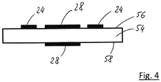
- the first antenna and / or the second antenna are arranged on a printed circuit board and in particular in the form of microstrip and / or patch antennas.
- the arrangement on a printed circuit board means that the antennas can be produced in a very space-saving manner and also very economically using modern processes for producing printed circuit boards, in particular in the same process as the other electronics of the safety switching device.
- the antennas preferably extend at least essentially only parallel to the surface of the printed circuit board (or within the printed circuit board) and thus do not form a significant increase. In this way, the safety switching device can be made particularly small and compact.
- the first and the second antenna and in particular all further antennas mentioned later can be arranged on the same printed circuit board.
- the first antenna and the second antenna are arranged on different layers of the same printed circuit board.
- the first and the second antenna are isolated from one another and / or galvanically isolated.
- the first antenna on a Front of the circuit board and the second antenna can be arranged on a back of the same circuit board.
- the use of different layers or layers of the printed circuit board ie a PCB - printed circuit board) enables the two antennas to be securely insulated from one another, in particular also allowing galvanic isolation between the first and second antennas with low manufacturing costs.
- the first and second antennas are arranged fixed to one another.
- the first and second antennas can also be arranged on the same layer of the printed circuit board.
- the first and second antennas are preferably spaced apart from one another and have no direct electrical connection.
- Electrical isolation is preferably achieved by using the two antennas, in particular between the monitoring unit and the switching element.
- Attaching the first and second antennas on the same circuit board also has the advantage that a transmission path for the test signal can be made very short and thus insensitive to external influences.
- a transmission path for the test signal can be made very short and thus insensitive to external influences.
- an influence on the test signal by the switching state of the electrical switching element can be detected more easily, since external influences on the test signal turn out to be very small and can therefore be essentially neglected.
- the space requirement of an individual circuit board is very small, so that both antennas also have only a small space requirement, as a result of which the safety switching device can in turn be made very compact.
- the second antenna is part of an oscillating circuit, the resonance frequency of which depends on the actual switching state of the switching element.
- the resonant circuit can comprise, for example, a capacitor and a coil, wherein the coil can be formed by the second antenna.
- the resonant circuit preferably also comprises one or more additional capacitive or inductive components which (only) are electrically coupled into the resonant circuit when the switching element is closed in order to change the resonant frequency of the resonant circuit.
- the additional components can thus be electrically connected to the switching element in such a way that the additional components become part of the resonant circuit in the closed switching state of the switching element.
- the additional coupling of a capacitance into the resonant circuit can reduce the resonant frequency of the resonant circuit.
- the resonant circuit can thus have two different resonance frequencies. The first resonance frequency is when the switching element is actually open and the second resonance frequency is when the switching element is actually closed.
- the resonant circuit can have a first resonance frequency when the switching element is closed and a second, different, resonance frequency when the switching element is open.
- the switching element can preferably be electrically coupled to the resonant circuit or, as mentioned above, be part of the resonant circuit. The actual switching state of the switching element can then be deduced by recognizing the resonance frequency.
- the resonant circuit can comprise the second antenna, which can have two electrical contacts, and a first capacitor, the first capacitor being connected between the two electrical contacts of the second antenna. This results in a parallel connection of the first capacitor with the second antenna.
- the switching element can also have two electrical contacts, with each of the electrical contacts of the switching element preferably being electrically connected to an electrical contact of the second antenna via an additional capacitor (i.e. for example a second and third capacitor).
- the second and third capacitors can accordingly be the additional components mentioned above.
- the test signal comprises at least two different transmission frequencies, which preferably correspond to the first and / or second resonance frequency.
- the transmission frequencies can also be referred to as carrier frequencies.
- the first and the second transmission frequency are transmitted in particular one after the other by the first antenna.
- the resonance circuit of the second antenna can be particularly strongly excited with a suitable switching state if the transmission and resonance frequencies match, which can be detected in a simple manner, which in turn makes the actual switching state of the switching element can be determined.
- the test signal and thus also the transmission frequencies are preferably generated by means of a signal generator and are coupled into the first antenna by the signal generator.
- a frequency ramp, a continuous frequency change or a wobbling of the transmission frequency can also be implemented by the signal generator.
- the transmission frequency and thus the test signal can also be modulated, for example by means of amplitudes or phase modulation. Modulation using on-off keying is also possible.
- the test signal can, for example, comprise a modulation according to the pattern on-off-on-on-off-on.
- NFC tag Near Field Communication Tag
- the safety switching device comprises one or more additional electrical switching elements.
- the actual switching state of the additional switching element or elements also influences the test signal.
- At least one of the additional electrical switching elements is preferably coupled to an additional resonant circuit, the resonance frequency of which depends on the actual switching state of the additional electrical switching element, the resonant frequency or the resonant frequencies of the additional resonant circuit preferably differing from the resonant frequency or the resonant frequencies of the resonant circuit.
- the additional oscillating circuit or circuits preferably each comprise a separate second antenna. However, several resonant circuits can also be connected to a second antenna.
- the additional electrical switching elements can be connected in series with the (first) electrical switching element in order to enable redundant disconnection of the electrical consumer. It is also possible for the additional electrical switching elements to be used to implement a multi-channel safety switching device which can switch different electrical consumers independently of one another.
- the safety switching device can have, for example, two or three channels, in each of which two electrical switching elements are connected in series. This results in a total of four or six electrical switching elements.
- Each of the switching elements can be part of a separate resonant circuit.
- the additional resonant circuits can also be switched back and forth between two resonance frequencies by the respective switching element changing its switching state between closed and open (or vice versa). All resonance frequencies used within the same safety switching device preferably differ, so that the actual switching state of each switching element can be clearly detected by means of only one first antenna, it also being clear from which switching element the respective resonance frequency "originates".
- the test signal can also include the resonance frequencies of the additional resonant circuits, so that each switching element can be checked separately for its actual switching state.
- the additional resonance frequencies in the test signal can be contained in the test signal one after the other in time.
- test signal it is also possible to use the test signal to detect only one switching state of the switching element or of the switching elements, in particular the "open" switching state.
- the test signal can be used as transmission frequencies, in particular only that include resonance frequencies that occur when the switching elements contained in the safety switching device are in the "open” switching state. If, for example, only one switching element is to be monitored, the test signal comprises or contains only exactly one transmission frequency.
- first antennas for the detection of the switching states of several different switching elements.
- a plurality of first antennas can also be provided, which interact with only one or also a plurality of second antennas.
- the second antennas or the resonant circuits, which interact with a respective first antenna only different resonance frequencies are preferably used.
- the first antenna spans an area within which the second antenna or the second antennas is / are arranged.
- the arrangement of the second antenna within the first antenna ensures safe and good transmission of the test signal.
- the first antenna shields the second antenna against external interference.
- the second antenna in the same plane or in parallel planes, e.g. in a layer below or above the first antenna, within the first antenna.
- the first and / or the second antenna are preferably planar.
- the first and second antenna as well as the monitoring unit and the switching element are in the same unit, preferably arranged within the same housing.
- the first and second antenna and the switching element are preferably arranged on the same circuit board. This in turn can promote a compact design of the safety switching device.
- the first antenna is designed to receive data by means of near field communication (NFC) and / or radio frequency identification (RFID).
- the monitoring unit preferably has an interface connected to the first antenna for communication by means of NFC and / or RFID.
- the first antenna can thus be used twice, on the one hand for determining the actual switching state of the electrical switching element or of a plurality of electrical switching elements and on the other hand for data communication using NFC and / or RFID.
- the data received or sent by the first antenna can be transmitted to / from the monitoring unit by means of the interface. In this way, the monitoring unit can, for example, output diagnostic / status data or receive configuration data.
- the safety switching device can be configured, for example, by means of a smartphone. Data can then also be read out using the smartphone, as a result of which the switching states or any errors can be determined.
- the first antenna can be designed to transmit test signals with a transmission frequency in the range from 100 to 500 kHz, preferably from 100 to 200 kHz.
- the first antenna can be designed for RFID communication in the long wave range at 125 kHz, 134 kHz, 250 kHz, 375 kHz, 500 kHz, 625 kHz, 750 kHz and / or 875 kHz.
- the first antenna can also be designed for RFID communication and / or for NFC communication at a frequency of 13.56 MHz. Also the actual switching states can be determined in the range of 13.56 MHz, ie the resonance frequencies can be in this range.
- the resonance frequencies can also be in the range between 100 and 500 kHz, preferably in the range between 100 and 200 kHz.
- the two resonance frequencies of the same resonant circuit (for closed and open switching states) differ by at least 20%, preferably by at least 10%. In this way, a reliable distinction between the two switching states is guaranteed.
- the switching state can also preferably be determined, in particular only, in the open switching state.
- the switched frequencies play no role, so that the frequencies switched by means of the safety switching device can be in the same range as the frequencies of the test signal or the resonance frequencies.
- the monitoring unit checks whether the switching element has really changed to the open switching state. If the actual switching state an error signal can be output from the desired or expected switching state. The error signal can then alert operating personnel or cause a higher-level control system to switch off the entire system in which the consumer is installed. The safety switching device itself can also use the error signal for switching off.
- diagnostic, status and / or configuration data of the safety switching device are received and / or transmitted by means of the first antenna, in particular by NFC and / or RFID.
- the received data preferably influence the operation of the safety switching device.
- the data sent include, in particular, information about the state of the safety switching device.
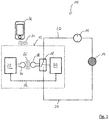
- a monitoring unit 22 is provided in the safety switching device 12 and is electrically connected to a first antenna 24.
- the first antenna 24 is designed to transmit a test signal 26 to a second antenna 28.
- the second antenna 28 is in turn electrically connected to the relay 18, the switching state of the relay 18 influencing the test signal 26, as will be explained in more detail below.
Landscapes
- Physics & Mathematics (AREA)
- Electromagnetism (AREA)
- Transmitters (AREA)
Priority Applications (1)
| Application Number | Priority Date | Filing Date | Title |
|---|---|---|---|
| EP18213553.3A EP3671797B1 (fr) | 2018-12-18 | 2018-12-18 | Dispositif de commutation de sécurité |
Applications Claiming Priority (1)
| Application Number | Priority Date | Filing Date | Title |
|---|---|---|---|
| EP18213553.3A EP3671797B1 (fr) | 2018-12-18 | 2018-12-18 | Dispositif de commutation de sécurité |
Publications (2)
| Publication Number | Publication Date |
|---|---|
| EP3671797A1 true EP3671797A1 (fr) | 2020-06-24 |
| EP3671797B1 EP3671797B1 (fr) | 2021-05-26 |
Family
ID=64744695
Family Applications (1)
| Application Number | Title | Priority Date | Filing Date |
|---|---|---|---|
| EP18213553.3A Active EP3671797B1 (fr) | 2018-12-18 | 2018-12-18 | Dispositif de commutation de sécurité |
Country Status (1)
| Country | Link |
|---|---|
| EP (1) | EP3671797B1 (fr) |
Cited By (1)
| Publication number | Priority date | Publication date | Assignee | Title |
|---|---|---|---|---|
| DE102023106235A1 (de) * | 2023-03-13 | 2024-09-19 | Wieland Electric Gmbh | Funktional sicherer Freigabepfad |
Citations (2)
| Publication number | Priority date | Publication date | Assignee | Title |
|---|---|---|---|---|
| US20020021226A1 (en) * | 2000-08-08 | 2002-02-21 | Philippe Clement | Electrical apparatus comprising a monitoring device, support and monitoring device for such an apparatus, and electrical installation incorporating them |
| DE10146753C1 (de) * | 2001-09-22 | 2003-04-24 | Pilz Gmbh & Co | Sicherheitsschaltvorrichtung zum sicheren Abschalten eines elektrischen Verbrauchers |
Family Cites Families (14)
| Publication number | Priority date | Publication date | Assignee | Title |
|---|---|---|---|---|
| FR2381384A1 (fr) | 1977-02-18 | 1978-09-15 | Crouzet Sa | Dispositif de controle operationnel d'un element contacteur electromecanique |
| FR2893745B1 (fr) | 2005-11-22 | 2007-12-21 | Schneider Electric Ind Sas | Dispositif et procede de surveillance de position d'au moins une partie mobile d'une pluralite d'appareils electriques et tableau incorporant un tel dispositif |
| FR2901426B1 (fr) | 2006-05-19 | 2008-09-12 | Schneider Electric Ind Sas | Dispositif de surveillance de position d'une partie mobile d'un appareil electrique interrupteur |
| US8061017B2 (en) | 2006-08-28 | 2011-11-22 | Avago Technologies Ecbu Ip (Singapore) Pte. Ltd. | Methods of making coil transducers |
| US8385043B2 (en) | 2006-08-28 | 2013-02-26 | Avago Technologies ECBU IP (Singapoare) Pte. Ltd. | Galvanic isolator |
| US8258911B2 (en) | 2008-03-31 | 2012-09-04 | Avago Technologies ECBU IP (Singapor) Pte. Ltd. | Compact power transformer components, devices, systems and methods |
| DE102009038996A1 (de) | 2008-08-28 | 2010-03-04 | Hirschmann Automotive Gmbh | Manipulationssicherer RFID-Schalter für die Anwendung in Fahrzeugen |
| DE102008057833B4 (de) | 2008-11-19 | 2011-12-22 | Semikron Elektronik Gmbh & Co. Kg | Leistungshalbleitermodul mit Steuerfunktionalität und integriertem Übertrager |
| DE102012003365B4 (de) | 2012-02-22 | 2014-12-18 | Phoenix Contact Gmbh & Co. Kg | Planarer eigensicherer Übertrager mit Schichtaufbau |
| US8964344B2 (en) | 2012-08-24 | 2015-02-24 | Schneider Electric USA, Inc. | Circuit breaker signaling system for control of an arc fault detection system |
| DE102013208989A1 (de) | 2012-08-29 | 2014-03-06 | Siemens Aktiengesellschaft | Elektromechanisches Schaltgerät und Anordnung zur Zustandserfassung eines elektromechanischen Schaltgerätes |
| US9331746B2 (en) | 2012-12-19 | 2016-05-03 | Eaton Corporation | System and method for providing information to and/or obtaining information from a component of an electrical distribution system |
| CN108780709B (zh) | 2016-05-18 | 2019-08-13 | 西门子股份公司 | 用于提供继电器触头的功能安全监测的系统和方法 |
| US10254323B2 (en) | 2016-06-30 | 2019-04-09 | General Electric Company | Passive wireless monitoring of individual capacitor cans |
-
2018
- 2018-12-18 EP EP18213553.3A patent/EP3671797B1/fr active Active
Patent Citations (2)
| Publication number | Priority date | Publication date | Assignee | Title |
|---|---|---|---|---|
| US20020021226A1 (en) * | 2000-08-08 | 2002-02-21 | Philippe Clement | Electrical apparatus comprising a monitoring device, support and monitoring device for such an apparatus, and electrical installation incorporating them |
| DE10146753C1 (de) * | 2001-09-22 | 2003-04-24 | Pilz Gmbh & Co | Sicherheitsschaltvorrichtung zum sicheren Abschalten eines elektrischen Verbrauchers |
Cited By (1)
| Publication number | Priority date | Publication date | Assignee | Title |
|---|---|---|---|---|
| DE102023106235A1 (de) * | 2023-03-13 | 2024-09-19 | Wieland Electric Gmbh | Funktional sicherer Freigabepfad |
Also Published As
| Publication number | Publication date |
|---|---|
| EP3671797B1 (fr) | 2021-05-26 |
Similar Documents
| Publication | Publication Date | Title |
|---|---|---|
| EP1673866B1 (fr) | Commutateur de protection, notamment commutateur d'arret d'urgence, pour deconnecter un dispositif dangereux | |
| DE10146753C1 (de) | Sicherheitsschaltvorrichtung zum sicheren Abschalten eines elektrischen Verbrauchers | |
| EP3053176B1 (fr) | Procédé et dispositif de surveillance d'au moins un contact de commande pour un véhicule | |
| DE2455923C2 (de) | Warnvorrichtung zum Melden eines Luftdruckabfalles in Fahrzeugreifen | |
| DE3347459C2 (fr) | ||
| DE10248640A1 (de) | Schaltgerät sowie System und Verfahren zur Signalübertragung zwischen diesem und einer Signalverarbeitungseinheit | |
| EP2868548B1 (fr) | Procédé de surveillance d'un état de commutation d'un commutateur d'un système de sécurisation de train et système de sécurisation de train | |
| DE3915188C1 (en) | Wireless interrogation and current supply method for switches - using capacitative and inductive elements corresp. to sec. winding of transformer | |
| EP3671797B1 (fr) | Dispositif de commutation de sécurité | |
| DE3905422C2 (fr) | ||
| EP1465221B1 (fr) | Agencement pour la surveillance d'un sélecteur de prises | |
| EP4125215B1 (fr) | Circuit électrique, en particulier pour un interrupteur de proximité à commande inductive | |
| EP4338182B1 (fr) | Appareil de surveillance de contact pour un contact de commutation tripolaire | |
| DE19933686A1 (de) | Schalter mit drahtloser Fernablesung | |
| EP2015964B1 (fr) | Marche pourvue d'un tapis de contact pour un vehicule ferroviaire | |
| DE10258919A1 (de) | Vorrichtung, System und Verfahren zur Schaltstellungssignalisierung eines Schaltgerätes | |
| DE10334061B4 (de) | Schaltungsanordnung und Verfahren zur Diagnose einer Antennenschaltung | |
| DE2148072C3 (de) | Schaltungsanordnung zur Überwachung von binären Signalen auf Antivalenz | |
| EP1726972A1 (fr) | Système de radar automobile et procédé destiné au fonctionnement d'un système de radar automobile | |
| EP1196311B1 (fr) | Systeme pour actionner des elements fonctionnels electriques | |
| DE19638956A1 (de) | Anschaltbaugruppe | |
| DE102004059694B3 (de) | Verfahren und Anordnungen zum Prüfen einer Antennenanordnung, insbesondere eines Kraftfahrzeuges | |
| DE102023106235A1 (de) | Funktional sicherer Freigabepfad | |
| DE2808403C2 (de) | Schaltung zum Auslösen eines Störungssignals | |
| DE102024117701A1 (de) | Sicherheits-Steuereinrichtung und Verfahren zum Betrieben einer solchen |
Legal Events
| Date | Code | Title | Description |
|---|---|---|---|
| PUAI | Public reference made under article 153(3) epc to a published international application that has entered the european phase |
Free format text: ORIGINAL CODE: 0009012 |
|
| STAA | Information on the status of an ep patent application or granted ep patent |
Free format text: STATUS: REQUEST FOR EXAMINATION WAS MADE |
|
| 17P | Request for examination filed |
Effective date: 20200326 |
|
| AK | Designated contracting states |
Kind code of ref document: A1 Designated state(s): AL AT BE BG CH CY CZ DE DK EE ES FI FR GB GR HR HU IE IS IT LI LT LU LV MC MK MT NL NO PL PT RO RS SE SI SK SM TR |
|
| AX | Request for extension of the european patent |
Extension state: BA ME |
|
| GRAP | Despatch of communication of intention to grant a patent |
Free format text: ORIGINAL CODE: EPIDOSNIGR1 |
|
| STAA | Information on the status of an ep patent application or granted ep patent |
Free format text: STATUS: GRANT OF PATENT IS INTENDED |
|
| INTG | Intention to grant announced |
Effective date: 20200729 |
|
| GRAJ | Information related to disapproval of communication of intention to grant by the applicant or resumption of examination proceedings by the epo deleted |
Free format text: ORIGINAL CODE: EPIDOSDIGR1 |
|
| STAA | Information on the status of an ep patent application or granted ep patent |
Free format text: STATUS: REQUEST FOR EXAMINATION WAS MADE |
|
| GRAP | Despatch of communication of intention to grant a patent |
Free format text: ORIGINAL CODE: EPIDOSNIGR1 |
|
| STAA | Information on the status of an ep patent application or granted ep patent |
Free format text: STATUS: GRANT OF PATENT IS INTENDED |
|
| INTC | Intention to grant announced (deleted) | ||
| INTG | Intention to grant announced |
Effective date: 20210127 |
|
| GRAS | Grant fee paid |
Free format text: ORIGINAL CODE: EPIDOSNIGR3 |
|
| GRAA | (expected) grant |
Free format text: ORIGINAL CODE: 0009210 |
|
| STAA | Information on the status of an ep patent application or granted ep patent |
Free format text: STATUS: THE PATENT HAS BEEN GRANTED |
|
| AK | Designated contracting states |
Kind code of ref document: B1 Designated state(s): AL AT BE BG CH CY CZ DE DK EE ES FI FR GB GR HR HU IE IS IT LI LT LU LV MC MK MT NL NO PL PT RO RS SE SI SK SM TR |
|
| REG | Reference to a national code |
Ref country code: GB Ref legal event code: FG4D Free format text: NOT ENGLISH |
|
| REG | Reference to a national code |
Ref country code: CH Ref legal event code: EP |
|
| REG | Reference to a national code |
Ref country code: AT Ref legal event code: REF Ref document number: 1397056 Country of ref document: AT Kind code of ref document: T Effective date: 20210615 |
|
| REG | Reference to a national code |
Ref country code: DE Ref legal event code: R096 Ref document number: 502018005418 Country of ref document: DE |
|
| REG | Reference to a national code |
Ref country code: IE Ref legal event code: FG4D Free format text: LANGUAGE OF EP DOCUMENT: GERMAN |
|
| REG | Reference to a national code |
Ref country code: LT Ref legal event code: MG9D |
|
| PG25 | Lapsed in a contracting state [announced via postgrant information from national office to epo] |
Ref country code: BG Free format text: LAPSE BECAUSE OF FAILURE TO SUBMIT A TRANSLATION OF THE DESCRIPTION OR TO PAY THE FEE WITHIN THE PRESCRIBED TIME-LIMIT Effective date: 20210826 Ref country code: FI Free format text: LAPSE BECAUSE OF FAILURE TO SUBMIT A TRANSLATION OF THE DESCRIPTION OR TO PAY THE FEE WITHIN THE PRESCRIBED TIME-LIMIT Effective date: 20210526 Ref country code: HR Free format text: LAPSE BECAUSE OF FAILURE TO SUBMIT A TRANSLATION OF THE DESCRIPTION OR TO PAY THE FEE WITHIN THE PRESCRIBED TIME-LIMIT Effective date: 20210526 Ref country code: LT Free format text: LAPSE BECAUSE OF FAILURE TO SUBMIT A TRANSLATION OF THE DESCRIPTION OR TO PAY THE FEE WITHIN THE PRESCRIBED TIME-LIMIT Effective date: 20210526 |
|
| REG | Reference to a national code |
Ref country code: NL Ref legal event code: MP Effective date: 20210526 |
|
| PG25 | Lapsed in a contracting state [announced via postgrant information from national office to epo] |
Ref country code: GR Free format text: LAPSE BECAUSE OF FAILURE TO SUBMIT A TRANSLATION OF THE DESCRIPTION OR TO PAY THE FEE WITHIN THE PRESCRIBED TIME-LIMIT Effective date: 20210827 Ref country code: IS Free format text: LAPSE BECAUSE OF FAILURE TO SUBMIT A TRANSLATION OF THE DESCRIPTION OR TO PAY THE FEE WITHIN THE PRESCRIBED TIME-LIMIT Effective date: 20210926 Ref country code: LV Free format text: LAPSE BECAUSE OF FAILURE TO SUBMIT A TRANSLATION OF THE DESCRIPTION OR TO PAY THE FEE WITHIN THE PRESCRIBED TIME-LIMIT Effective date: 20210526 Ref country code: PL Free format text: LAPSE BECAUSE OF FAILURE TO SUBMIT A TRANSLATION OF THE DESCRIPTION OR TO PAY THE FEE WITHIN THE PRESCRIBED TIME-LIMIT Effective date: 20210526 Ref country code: PT Free format text: LAPSE BECAUSE OF FAILURE TO SUBMIT A TRANSLATION OF THE DESCRIPTION OR TO PAY THE FEE WITHIN THE PRESCRIBED TIME-LIMIT Effective date: 20210927 Ref country code: NO Free format text: LAPSE BECAUSE OF FAILURE TO SUBMIT A TRANSLATION OF THE DESCRIPTION OR TO PAY THE FEE WITHIN THE PRESCRIBED TIME-LIMIT Effective date: 20210826 Ref country code: RS Free format text: LAPSE BECAUSE OF FAILURE TO SUBMIT A TRANSLATION OF THE DESCRIPTION OR TO PAY THE FEE WITHIN THE PRESCRIBED TIME-LIMIT Effective date: 20210526 Ref country code: SE Free format text: LAPSE BECAUSE OF FAILURE TO SUBMIT A TRANSLATION OF THE DESCRIPTION OR TO PAY THE FEE WITHIN THE PRESCRIBED TIME-LIMIT Effective date: 20210526 |
|
| PG25 | Lapsed in a contracting state [announced via postgrant information from national office to epo] |
Ref country code: NL Free format text: LAPSE BECAUSE OF FAILURE TO SUBMIT A TRANSLATION OF THE DESCRIPTION OR TO PAY THE FEE WITHIN THE PRESCRIBED TIME-LIMIT Effective date: 20210526 |
|
| PG25 | Lapsed in a contracting state [announced via postgrant information from national office to epo] |
Ref country code: ES Free format text: LAPSE BECAUSE OF FAILURE TO SUBMIT A TRANSLATION OF THE DESCRIPTION OR TO PAY THE FEE WITHIN THE PRESCRIBED TIME-LIMIT Effective date: 20210526 Ref country code: EE Free format text: LAPSE BECAUSE OF FAILURE TO SUBMIT A TRANSLATION OF THE DESCRIPTION OR TO PAY THE FEE WITHIN THE PRESCRIBED TIME-LIMIT Effective date: 20210526 Ref country code: SK Free format text: LAPSE BECAUSE OF FAILURE TO SUBMIT A TRANSLATION OF THE DESCRIPTION OR TO PAY THE FEE WITHIN THE PRESCRIBED TIME-LIMIT Effective date: 20210526 Ref country code: SM Free format text: LAPSE BECAUSE OF FAILURE TO SUBMIT A TRANSLATION OF THE DESCRIPTION OR TO PAY THE FEE WITHIN THE PRESCRIBED TIME-LIMIT Effective date: 20210526 Ref country code: CZ Free format text: LAPSE BECAUSE OF FAILURE TO SUBMIT A TRANSLATION OF THE DESCRIPTION OR TO PAY THE FEE WITHIN THE PRESCRIBED TIME-LIMIT Effective date: 20210526 Ref country code: DK Free format text: LAPSE BECAUSE OF FAILURE TO SUBMIT A TRANSLATION OF THE DESCRIPTION OR TO PAY THE FEE WITHIN THE PRESCRIBED TIME-LIMIT Effective date: 20210526 Ref country code: RO Free format text: LAPSE BECAUSE OF FAILURE TO SUBMIT A TRANSLATION OF THE DESCRIPTION OR TO PAY THE FEE WITHIN THE PRESCRIBED TIME-LIMIT Effective date: 20210526 |
|
| REG | Reference to a national code |
Ref country code: DE Ref legal event code: R026 Ref document number: 502018005418 Country of ref document: DE |
|
| PLBI | Opposition filed |
Free format text: ORIGINAL CODE: 0009260 |
|
| PLAX | Notice of opposition and request to file observation + time limit sent |
Free format text: ORIGINAL CODE: EPIDOSNOBS2 |
|
| 26 | Opposition filed |
Opponent name: PHOENIX CONTACT GMBH & CO. KG Effective date: 20220225 |
|
| PG25 | Lapsed in a contracting state [announced via postgrant information from national office to epo] |
Ref country code: IS Free format text: LAPSE BECAUSE OF FAILURE TO SUBMIT A TRANSLATION OF THE DESCRIPTION OR TO PAY THE FEE WITHIN THE PRESCRIBED TIME-LIMIT Effective date: 20210926 Ref country code: AL Free format text: LAPSE BECAUSE OF FAILURE TO SUBMIT A TRANSLATION OF THE DESCRIPTION OR TO PAY THE FEE WITHIN THE PRESCRIBED TIME-LIMIT Effective date: 20210526 |
|
| PLBB | Reply of patent proprietor to notice(s) of opposition received |
Free format text: ORIGINAL CODE: EPIDOSNOBS3 |
|
| PG25 | Lapsed in a contracting state [announced via postgrant information from national office to epo] |
Ref country code: MC Free format text: LAPSE BECAUSE OF FAILURE TO SUBMIT A TRANSLATION OF THE DESCRIPTION OR TO PAY THE FEE WITHIN THE PRESCRIBED TIME-LIMIT Effective date: 20210526 |
|
| REG | Reference to a national code |
Ref country code: CH Ref legal event code: PL |
|
| REG | Reference to a national code |
Ref country code: BE Ref legal event code: MM Effective date: 20211231 |
|
| PG25 | Lapsed in a contracting state [announced via postgrant information from national office to epo] |
Ref country code: LU Free format text: LAPSE BECAUSE OF NON-PAYMENT OF DUE FEES Effective date: 20211218 Ref country code: IE Free format text: LAPSE BECAUSE OF NON-PAYMENT OF DUE FEES Effective date: 20211218 |
|
| PG25 | Lapsed in a contracting state [announced via postgrant information from national office to epo] |
Ref country code: BE Free format text: LAPSE BECAUSE OF NON-PAYMENT OF DUE FEES Effective date: 20211231 |
|
| PG25 | Lapsed in a contracting state [announced via postgrant information from national office to epo] |
Ref country code: LI Free format text: LAPSE BECAUSE OF NON-PAYMENT OF DUE FEES Effective date: 20211231 Ref country code: CH Free format text: LAPSE BECAUSE OF NON-PAYMENT OF DUE FEES Effective date: 20211231 |
|
| PG25 | Lapsed in a contracting state [announced via postgrant information from national office to epo] |
Ref country code: CY Free format text: LAPSE BECAUSE OF FAILURE TO SUBMIT A TRANSLATION OF THE DESCRIPTION OR TO PAY THE FEE WITHIN THE PRESCRIBED TIME-LIMIT Effective date: 20210526 |
|
| PG25 | Lapsed in a contracting state [announced via postgrant information from national office to epo] |
Ref country code: HU Free format text: LAPSE BECAUSE OF FAILURE TO SUBMIT A TRANSLATION OF THE DESCRIPTION OR TO PAY THE FEE WITHIN THE PRESCRIBED TIME-LIMIT; INVALID AB INITIO Effective date: 20181218 |
|
| GBPC | Gb: european patent ceased through non-payment of renewal fee |
Effective date: 20221218 |
|
| P01 | Opt-out of the competence of the unified patent court (upc) registered |
Effective date: 20230803 |
|
| PG25 | Lapsed in a contracting state [announced via postgrant information from national office to epo] |
Ref country code: GB Free format text: LAPSE BECAUSE OF NON-PAYMENT OF DUE FEES Effective date: 20221218 |
|
| PG25 | Lapsed in a contracting state [announced via postgrant information from national office to epo] |
Ref country code: MK Free format text: LAPSE BECAUSE OF FAILURE TO SUBMIT A TRANSLATION OF THE DESCRIPTION OR TO PAY THE FEE WITHIN THE PRESCRIBED TIME-LIMIT Effective date: 20210526 |
|
| PG25 | Lapsed in a contracting state [announced via postgrant information from national office to epo] |
Ref country code: TR Free format text: LAPSE BECAUSE OF FAILURE TO SUBMIT A TRANSLATION OF THE DESCRIPTION OR TO PAY THE FEE WITHIN THE PRESCRIBED TIME-LIMIT Effective date: 20210526 |
|
| PG25 | Lapsed in a contracting state [announced via postgrant information from national office to epo] |
Ref country code: MT Free format text: LAPSE BECAUSE OF FAILURE TO SUBMIT A TRANSLATION OF THE DESCRIPTION OR TO PAY THE FEE WITHIN THE PRESCRIBED TIME-LIMIT Effective date: 20210526 |
|
| REG | Reference to a national code |
Ref country code: DE Ref legal event code: R100 Ref document number: 502018005418 Country of ref document: DE |
|
| PLAG | Information modified related to despatch of communication that opposition is rejected |
Free format text: ORIGINAL CODE: EPIDOSCREJ1 |
|
| PLCK | Communication despatched that opposition was rejected |
Free format text: ORIGINAL CODE: EPIDOSNREJ1 |
|
| PLBN | Opposition rejected |
Free format text: ORIGINAL CODE: 0009273 |
|
| STAA | Information on the status of an ep patent application or granted ep patent |
Free format text: STATUS: OPPOSITION REJECTED |
|
| REG | Reference to a national code |
Ref country code: AT Ref legal event code: MM01 Ref document number: 1397056 Country of ref document: AT Kind code of ref document: T Effective date: 20231218 |
|
| 27O | Opposition rejected |
Effective date: 20241010 |
|
| PG25 | Lapsed in a contracting state [announced via postgrant information from national office to epo] |
Ref country code: AT Free format text: LAPSE BECAUSE OF NON-PAYMENT OF DUE FEES Effective date: 20231218 |
|
| PGFP | Annual fee paid to national office [announced via postgrant information from national office to epo] |
Ref country code: IT Payment date: 20251223 Year of fee payment: 8 |
|
| PGFP | Annual fee paid to national office [announced via postgrant information from national office to epo] |
Ref country code: FR Payment date: 20251229 Year of fee payment: 8 |
|
| PGFP | Annual fee paid to national office [announced via postgrant information from national office to epo] |
Ref country code: DE Payment date: 20260224 Year of fee payment: 8 |
|
| PGFP | Annual fee paid to national office [announced via postgrant information from national office to epo] |
Ref country code: AT Payment date: 20260410 Year of fee payment: 5 |