EP3671831B1 - Halbleiterpaketstruktur - Google Patents
Halbleiterpaketstruktur Download PDFInfo
- Publication number
- EP3671831B1 EP3671831B1 EP19213567.1A EP19213567A EP3671831B1 EP 3671831 B1 EP3671831 B1 EP 3671831B1 EP 19213567 A EP19213567 A EP 19213567A EP 3671831 B1 EP3671831 B1 EP 3671831B1
- Authority
- EP
- European Patent Office
- Prior art keywords
- substrate
- package structure
- semiconductor package
- semiconductor
- holes
- Prior art date
- Legal status (The legal status is an assumption and is not a legal conclusion. Google has not performed a legal analysis and makes no representation as to the accuracy of the status listed.)
- Active
Links
Images






Classifications
-
- H—ELECTRICITY
- H10—SEMICONDUCTOR DEVICES; ELECTRIC SOLID-STATE DEVICES NOT OTHERWISE PROVIDED FOR
- H10W—GENERIC PACKAGES, INTERCONNECTIONS, CONNECTORS OR OTHER CONSTRUCTIONAL DETAILS OF DEVICES COVERED BY CLASS H10
- H10W90/00—Package configurations
- H10W90/701—Package configurations characterised by the relative positions of pads or connectors relative to package parts
-
- H—ELECTRICITY
- H10—SEMICONDUCTOR DEVICES; ELECTRIC SOLID-STATE DEVICES NOT OTHERWISE PROVIDED FOR
- H10W—GENERIC PACKAGES, INTERCONNECTIONS, CONNECTORS OR OTHER CONSTRUCTIONAL DETAILS OF DEVICES COVERED BY CLASS H10
- H10W40/00—Arrangements for thermal protection or thermal control
- H10W40/10—Arrangements for heating
-
- H—ELECTRICITY
- H10—SEMICONDUCTOR DEVICES; ELECTRIC SOLID-STATE DEVICES NOT OTHERWISE PROVIDED FOR
- H10W—GENERIC PACKAGES, INTERCONNECTIONS, CONNECTORS OR OTHER CONSTRUCTIONAL DETAILS OF DEVICES COVERED BY CLASS H10
- H10W42/00—Arrangements for protection of devices
- H10W42/121—Arrangements for protection of devices protecting against mechanical damage
-
- H—ELECTRICITY
- H10—SEMICONDUCTOR DEVICES; ELECTRIC SOLID-STATE DEVICES NOT OTHERWISE PROVIDED FOR
- H10W—GENERIC PACKAGES, INTERCONNECTIONS, CONNECTORS OR OTHER CONSTRUCTIONAL DETAILS OF DEVICES COVERED BY CLASS H10
- H10W74/00—Encapsulations, e.g. protective coatings
- H10W74/10—Encapsulations, e.g. protective coatings characterised by their shape or disposition
- H10W74/111—Encapsulations, e.g. protective coatings characterised by their shape or disposition the semiconductor body being completely enclosed
- H10W74/121—Encapsulations, e.g. protective coatings characterised by their shape or disposition the semiconductor body being completely enclosed by multiple encapsulations, e.g. by a thin protective coating and a thick encapsulation
-
- H—ELECTRICITY
- H10—SEMICONDUCTOR DEVICES; ELECTRIC SOLID-STATE DEVICES NOT OTHERWISE PROVIDED FOR
- H10W—GENERIC PACKAGES, INTERCONNECTIONS, CONNECTORS OR OTHER CONSTRUCTIONAL DETAILS OF DEVICES COVERED BY CLASS H10
- H10W90/00—Package configurations
-
- H—ELECTRICITY
- H10—SEMICONDUCTOR DEVICES; ELECTRIC SOLID-STATE DEVICES NOT OTHERWISE PROVIDED FOR
- H10W—GENERIC PACKAGES, INTERCONNECTIONS, CONNECTORS OR OTHER CONSTRUCTIONAL DETAILS OF DEVICES COVERED BY CLASS H10
- H10W70/00—Package substrates; Interposers; Redistribution layers [RDL]
- H10W70/60—Insulating or insulated package substrates; Interposers; Redistribution layers
-
- H—ELECTRICITY
- H10—SEMICONDUCTOR DEVICES; ELECTRIC SOLID-STATE DEVICES NOT OTHERWISE PROVIDED FOR
- H10W—GENERIC PACKAGES, INTERCONNECTIONS, CONNECTORS OR OTHER CONSTRUCTIONAL DETAILS OF DEVICES COVERED BY CLASS H10
- H10W70/00—Package substrates; Interposers; Redistribution layers [RDL]
- H10W70/60—Insulating or insulated package substrates; Interposers; Redistribution layers
- H10W70/611—Insulating or insulated package substrates; Interposers; Redistribution layers for connecting multiple chips together
-
- H—ELECTRICITY
- H10—SEMICONDUCTOR DEVICES; ELECTRIC SOLID-STATE DEVICES NOT OTHERWISE PROVIDED FOR
- H10W—GENERIC PACKAGES, INTERCONNECTIONS, CONNECTORS OR OTHER CONSTRUCTIONAL DETAILS OF DEVICES COVERED BY CLASS H10
- H10W70/00—Package substrates; Interposers; Redistribution layers [RDL]
- H10W70/60—Insulating or insulated package substrates; Interposers; Redistribution layers
- H10W70/62—Insulating or insulated package substrates; Interposers; Redistribution layers characterised by their interconnections
- H10W70/65—Shapes or dispositions of interconnections
-
- H—ELECTRICITY
- H10—SEMICONDUCTOR DEVICES; ELECTRIC SOLID-STATE DEVICES NOT OTHERWISE PROVIDED FOR
- H10W—GENERIC PACKAGES, INTERCONNECTIONS, CONNECTORS OR OTHER CONSTRUCTIONAL DETAILS OF DEVICES COVERED BY CLASS H10
- H10W70/00—Package substrates; Interposers; Redistribution layers [RDL]
- H10W70/60—Insulating or insulated package substrates; Interposers; Redistribution layers
- H10W70/62—Insulating or insulated package substrates; Interposers; Redistribution layers characterised by their interconnections
- H10W70/65—Shapes or dispositions of interconnections
- H10W70/652—Cross-sectional shapes
-
- H—ELECTRICITY
- H10—SEMICONDUCTOR DEVICES; ELECTRIC SOLID-STATE DEVICES NOT OTHERWISE PROVIDED FOR
- H10W—GENERIC PACKAGES, INTERCONNECTIONS, CONNECTORS OR OTHER CONSTRUCTIONAL DETAILS OF DEVICES COVERED BY CLASS H10
- H10W70/00—Package substrates; Interposers; Redistribution layers [RDL]
- H10W70/60—Insulating or insulated package substrates; Interposers; Redistribution layers
- H10W70/62—Insulating or insulated package substrates; Interposers; Redistribution layers characterised by their interconnections
- H10W70/65—Shapes or dispositions of interconnections
- H10W70/654—Top-view layouts
- H10W70/655—Fan-out layouts
-
- H—ELECTRICITY
- H10—SEMICONDUCTOR DEVICES; ELECTRIC SOLID-STATE DEVICES NOT OTHERWISE PROVIDED FOR
- H10W—GENERIC PACKAGES, INTERCONNECTIONS, CONNECTORS OR OTHER CONSTRUCTIONAL DETAILS OF DEVICES COVERED BY CLASS H10
- H10W70/00—Package substrates; Interposers; Redistribution layers [RDL]
- H10W70/60—Insulating or insulated package substrates; Interposers; Redistribution layers
- H10W70/67—Insulating or insulated package substrates; Interposers; Redistribution layers characterised by their insulating layers or insulating parts
- H10W70/68—Shapes or dispositions thereof
-
- H—ELECTRICITY
- H10—SEMICONDUCTOR DEVICES; ELECTRIC SOLID-STATE DEVICES NOT OTHERWISE PROVIDED FOR
- H10W—GENERIC PACKAGES, INTERCONNECTIONS, CONNECTORS OR OTHER CONSTRUCTIONAL DETAILS OF DEVICES COVERED BY CLASS H10
- H10W70/00—Package substrates; Interposers; Redistribution layers [RDL]
- H10W70/60—Insulating or insulated package substrates; Interposers; Redistribution layers
- H10W70/67—Insulating or insulated package substrates; Interposers; Redistribution layers characterised by their insulating layers or insulating parts
- H10W70/68—Shapes or dispositions thereof
- H10W70/685—Shapes or dispositions thereof comprising multiple insulating layers
-
- H—ELECTRICITY
- H10—SEMICONDUCTOR DEVICES; ELECTRIC SOLID-STATE DEVICES NOT OTHERWISE PROVIDED FOR
- H10W—GENERIC PACKAGES, INTERCONNECTIONS, CONNECTORS OR OTHER CONSTRUCTIONAL DETAILS OF DEVICES COVERED BY CLASS H10
- H10W72/00—Interconnections or connectors in packages
- H10W72/20—Bump connectors, e.g. solder bumps or copper pillars; Dummy bumps; Thermal bumps
- H10W72/221—Structures or relative sizes
-
- H—ELECTRICITY
- H10—SEMICONDUCTOR DEVICES; ELECTRIC SOLID-STATE DEVICES NOT OTHERWISE PROVIDED FOR
- H10W—GENERIC PACKAGES, INTERCONNECTIONS, CONNECTORS OR OTHER CONSTRUCTIONAL DETAILS OF DEVICES COVERED BY CLASS H10
- H10W74/00—Encapsulations, e.g. protective coatings
- H10W74/10—Encapsulations, e.g. protective coatings characterised by their shape or disposition
- H10W74/111—Encapsulations, e.g. protective coatings characterised by their shape or disposition the semiconductor body being completely enclosed
- H10W74/114—Encapsulations, e.g. protective coatings characterised by their shape or disposition the semiconductor body being completely enclosed by a substrate and the encapsulations
- H10W74/117—Encapsulations, e.g. protective coatings characterised by their shape or disposition the semiconductor body being completely enclosed by a substrate and the encapsulations the substrate having spherical bumps for external connection
-
- H—ELECTRICITY
- H10—SEMICONDUCTOR DEVICES; ELECTRIC SOLID-STATE DEVICES NOT OTHERWISE PROVIDED FOR
- H10W—GENERIC PACKAGES, INTERCONNECTIONS, CONNECTORS OR OTHER CONSTRUCTIONAL DETAILS OF DEVICES COVERED BY CLASS H10
- H10W90/00—Package configurations
- H10W90/701—Package configurations characterised by the relative positions of pads or connectors relative to package parts
- H10W90/721—Package configurations characterised by the relative positions of pads or connectors relative to package parts of bump connectors
- H10W90/724—Package configurations characterised by the relative positions of pads or connectors relative to package parts of bump connectors between a chip and a stacked insulating package substrate, interposer or RDL
Definitions
- the present invention relates to a semiconductor package structure.
- a semiconductor package can not only provide a semiconductor die with protection from environmental contaminants, but it can also provide an electrical connection between the semiconductor die packaged therein and a substrate, such as a printed circuit board (PCB).
- a semiconductor die may be enclosed in an encapsulating material, and traces are electrically connected to the semiconductor die and the substrate.
- a problem with such a semiconductor package is that it is subject to different temperatures during the packaging process.
- the semiconductor package may be highly stressed due to the different coefficients of thermal expansion (CTEs) of the various substrate and semiconductor die materials.
- CTEs coefficients of thermal expansion
- the semiconductor package may exhibit warping or cracking so that the electrical connection between the semiconductor die and the substrate may be damaged, and the reliability of the semiconductor package may be decreased.
- a configuration of a semiconductor device in which a heat-sink is in contact with a die is known from US 2018/204807 A1 .
- this document discloses a buffer layer disposed over a substrate and located between a frame and a semiconductor die.
- the invention refers to a semiconductor package structure according to claim 1. Preferred embodiments of the invention are defined in the appended dependent claims.
- Fig. 1A is a cross-sectional view of a semiconductor package structure 100a, in accordance with some examples not corresponding to the invention as defined in the claims but useful for the understanding thereof.
- Fig. 1C is a plan view of an arrangement of holes in a substrate 101 of the semiconductor package structure 100a shown in Fig. 1A
- Fig. 1A is a cross-sectional view of the semiconductor package structure 100a along line I-I' of Fig. 1C .
- the semiconductor package structure 100a may include a wafer-level semiconductor package, for example, a flip-chip semiconductor package.
- the semiconductor package structure 100a may be mounted on a base (not shown).
- the semiconductor package structure 100a may be a system-on-chip (SOC) package structure.
- the base may include a printed circuit board (PCB) and may be formed of polypropylene (PP).
- the base may include a package substrate.
- the semiconductor package structure 100a is mounted on the base by a bonding process.
- the semiconductor package structure 100a includes bump structures 111.
- the bump structures 111 may be conductive ball structures (such as ball grid array (BGA)), conductive pillar structures, or conductive paste structures that are mounted on and electrically coupled to the base in the bonding process.
- BGA ball grid array
- the semiconductor package structure 100a includes a substrate 101.
- the substrate 101 has a wiring structure therein.
- the wiring structure in the substrate 101 is a fan-out structure, and may include one or more conductive pads 103, conductive vias 105, conductive layers 107 and conductive pillars 109.
- the wiring structure in the substrate 101 may be disposed in one or more inter-metal dielectric (IMD) layers.
- the IMD layers may be formed of organic materials, which include a polymer base material, non-organic materials, which include silicon nitride (SiN x ), silicon oxide (SiO x ), grapheme, or the like.
- the IMD layers are made of a polymer base material. It should be noted that the number and configuration of the IMD layers, the conductive pads 103, the conductive vias 105, the conductive layers 107 and the conductive pillars 109 shown in Figures and only some examples and are not limitations to the present invention.
- the semiconductor package structure 100a also includes a first semiconductor die 115a and a second semiconductor die 115b bonded onto the substrate 101 through a plurality of conductive structures 119.
- the substrate 101 has a first surface 101a and a second surface 101b opposite thereto, the first surface 101a is facing the first semiconductor die 115a and the second semiconductor die 115b, and the second surface 101b is facing the above-mentioned base.
- the conductive structures 119 are disposed over the first surface 101a and below the first semiconductor die 115a and the second semiconductor die 115b, and the bump structures 111 are disposed over the second surface 101b of the substrate 101.
- the first semiconductor die 115a and the second semiconductor die 115b are electrically coupled to the bump structures 111 through the conductive structures 119 and the wiring structure in the substrate 101.
- the conductive structures 119 may be controlled collapse chip connection (C4) structures. It should be noted that the number of semiconductor dies integrated in the semiconductor package structure 100a is not limited to that disclosed in the embodiment.
- the first semiconductor die 115a and the second semiconductor die 115b are active devices.
- the first semiconductor die 115a and the second semiconductor die 115b may be logic dies including a central processing unit (CPU), a graphics processing unit (GPU), a dynamic random access memory (DRAM) controller or any combination thereof.
- one or more passive devices are also bonded onto the substrate 101.
- the first semiconductor die 115a and the second semiconductor dies 115b are arranged side-by-side. In some embodiments, the first semiconductor die 115a and the second semiconductor dies 115b are separated by a molding material 117.
- the molding material 117 surrounds the first semiconductor die 115a and the second semiconductor die 115b, and adjoins the sidewalls of the first semiconductor die 115a and the second semiconductor die 115b.
- the molding material 117 includes a nonconductive material such as an epoxy, a resin, a moldable polymer, or another suitable molding material. In some embodiments, the molding material 117 is applied as a substantial liquid, and then is cured through a chemical reaction.
- the molding material 117 is an ultraviolet (UV) or thermally cured polymer applied as a gel or malleable solid, and then is cured through a UV or thermal curing process.
- the molding material 117 may be cured with a mold (not shown).
- the surfaces of the first semiconductor die 115a and the second semiconductor dies 115b facing away from the first surface 101a of the substrate 101 are exposed by the molding material 117, such that a heat dissipating device (not shown) can directly attached to the surfaces of the first semiconductor die 115a and the second semiconductor dies 115b.
- a heat dissipating device (not shown) can directly attached to the surfaces of the first semiconductor die 115a and the second semiconductor dies 115b.
- the semiconductor package structure 100a also includes a polymer material 121 disposed under the molding material 117, the first semiconductor die 115a and the second semiconductor die 115b, and between the conductive structures 119.
- the semiconductor package structure 100a further includes an underfill layer 123 interposed between the first surface 101a of the substrate 101 and the polymer material 121.
- the first semiconductor die 115a, the second semiconductor dies 115b and the molding material 117 are surrounded by the underfill layer 123.
- the polymer material 121 and the underfill layer 123 are disposed to compensate for differing coefficients of thermal expansion (CTEs) between the substrate 101, the conductive structures 119, the first semiconductor die 115a and the second semiconductor dies 115b.
- CTEs coefficients of thermal expansion
- the semiconductor package structure 100a includes a frame 113 attached to the first surface 101a of the substrate 101 through an adhesive layer 112.
- the first semiconductor die 115a and the second semiconductor die 115b are surrounded by the frame 113 and the adhesive layer 112.
- the frame 113 and the adhesive layer 112 are separated from the underfill layer 121 by a gap.
- the substrate 101 has a first edge 101E 1 and a second edge 101E 2 opposite thereto.
- the first edge 101 E 1 and the second edge 101E 2 are coplanar with sidewalls of the frame 113and the adhesive layer 112.
- the substrate 101 of the semiconductor package structure 100a includes a first hole 110a and a second hole 110b formed on the second surface 101b.
- at least one of the first hole 110a and the second hole 110b penetrates through the substrate 101 from the first surface 101a to the second surface 101b.
- both the first hole 110a and the second hole 110b shown in Fig. 1A penetrate through the substrate 101, in some other embodiments, both the first hole 110a and the second hole 110b do not penetrate through the substrate 101 from the first surface 101a to the second surface 101b.
- the first hole 110a is covered by the first semiconductor die 115a
- the second hole 110b is covered by the second semiconductor die 115b.
- the first hole 110a is located within the projection of the first semiconductor die 115a on the substrate 101
- the second hole 110b is located within the projection of the second semiconductor die 115b on the substrate 101.
- the first semiconductor die 115a and the second semiconductor die 115b have a center line C-C' between them.
- the first hole 110a is disposed closer to the center line C-C' than the first edge 101E 1 of the substrate 101
- the second hole 110b is disposed closer to the center line C-C' than the second edge 101E 2 of the substrate 101.
- the first hole 110a and the second hole 110b are formed by a laser drilling process or another suitable process. It should be noted that the first hole 110a and the second hole 110b may be formed by the same forming process for the conductive pillars 109 in the wiring structure of the substrate 101. Moreover, the first semiconductor die 115a and the second semiconductor die 115b are bonded to the substrate 101 after forming the holes in the substrate 101. Therefore, the damage of the first semiconductor die 115a and the second semiconductor die 115b can be prevented.
- Fig. 1C is a plan view of an arrangement of holes in a substrate 101 of the semiconductor package structure 100a shown in Fig. 1A
- Fig. 1A is a cross-sectional view of the semiconductor package structure 100a along line I-I' of Fig. 1C
- Fig. 1C is the plan view from the bottom of the semiconductor package structure 100a.
- Fig. 1C is the plan view from the second surface 101b of the substrate 101, which the bump structures 111 are disposed on.
- the bump structures 111 are omitted for brevity.
- the substrate 101 includes more than two holes.
- the substrate 101 further includes a third hole 110c and the fourth hole 110d formed on the second surface 101b.
- the third hole 110c is covered by the first semiconductor die 115a
- the fourth hole 110d is covered by the second semiconductor die 115b.
- the substrate 101 has a center 101C, and the first hole 101a, the second hole 101b, the third hole 110c, and the fourth hole 110d are disposed closer to the center 101C than the first edge 101E 1 and the second edge 101E 2 of the substrate 101.
- the holes formed in the substrate 101 are designed to release the stress in the substrate 101, especially the stress concentrated in the region below the interface between two semiconductor dies (i.e. the first semiconductor die 115a and the second semiconductor die 115b). Since the semiconductor package structure 100a may be highly stressed due to the different coefficients of thermal expansion (CTEs) of the substrate 101 and the semiconductor dies, the holes formed in the substrate 101 can solve the warping or cracking problems caused by mismatched CTEs. As a result, the electrical connection within the semiconductor package structure 100a may not be damaged, and the reliability of the semiconductor package structure 100a may be increased.
- CTEs coefficients of thermal expansion
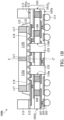
- Fig. 1B is a cross-sectional view of a semiconductor package structure 100b, in accordance with some other examples not corresponding to the invention as defined in the claims but useful for the understanding thereof. Descriptions of elements of the embodiments hereinafter that are the same as or similar to those previously described with reference to Fig. 1A are omitted for brevity.
- the semiconductor package structure 100b includes a stress buffer layer 125 filled in the first hole 110a and the second hole 110b.
- the stress buffer layer 125 is made of a polymer material, such as a silicone resin or rubber.
- the stress buffer layer 125 is made of an organic resin, such as Ajinomoto Build-up Film (ABF).
- the stress buffer layer 125 may be formed by a spin coating process. In some other embodiments, a material of the stress buffer layer 125 may be dispensed in the first hole 110a and the second hole 1 10b, and an excess portion of the material of the stress buffer layer 125 may be removed. In some embodiments, the stress buffer layer 125 may be formed before bonding the first semiconductor die 115a and the second semiconductor die 115b to the substrate 101.
- the stress buffer layer 125 may filled up the first hole 110a and the second hole 110b, and the surfaces of the stress buffer layer 125 are level with the second surface 101b of the substrate 101. In some other embodiments, the surfaces of the stress buffer layer 125 may not be level with the second surface 101b of the substrate 101 according to the actual manufacturing processes.
- Filling the first hole 110a and the second hole 110b with the stress buffer layer 125 may offer advantages like preventing the impurities and dust from dropping into the first hole 110a and the second hole 110b during the process of handling the substrate 101.
- the warping or cracking caused by mismatched coefficients of thermal expansion in the semiconductor package structure 100b can be solved by the holes (including the first hole 110a and the second hole 110b) and the stress buffer layer 125 formed in the substrate 101. Accordingly, the electrical connection within the semiconductor package structure 100b may not be damaged, and the lifespan of the semiconductor package structure 100b may be increased.
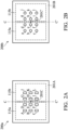
- Fig. 2A is a plan view showing shapes of holes in a substrate 201A of a semiconductor package structure 200a
- Fig. 2B is a plan view showing shapes of holes in a substrate 201B of a semiconductor package structure 200b, in accordance with some embodiments of the invention. Descriptions of elements of the embodiments hereinafter that are the same as or similar to those previously described with reference to Fig. 1C are omitted for brevity.
- the semiconductor package structure 200a has holes A, B, C, D, E, F, G, H, I, J, K and L in the substrate 201A, and the number of holes in the substrate 201A is much more than that in the substrate 101 of the semiconductor package structure 100a.
- the holes A, B, C, D, E and F are covered by the first semiconductor die 115a
- the holes G, H, I, J, K and L are covered by the second semiconductor die 115b.
- the holes A-F are located within the projection of the first semiconductor die 115a on the substrate 201A
- the holes G-L are located within the projection of the second semiconductor die 115b on the substrate 201A.
- the holes A, B and C are arranged in a first array
- the holes D, E and F are arranged in a second array
- the holes G, H and I are arranged in a third array
- the holes J, K and L are arranged in a fourth array.
- the first array, the second array, the third array and the fourth array are parallel to the center line C-C' of the first semiconductor die 115a and the second semiconductor die 115b.
- the substrate 201B in the semiconductor package structure 200b has holes a, b, c, d, e, f, g, h, i, j, k and l, which are arranged in the same way as the holes A-L of the substrate 201A in the semiconductor package structure 200a.
- the difference between the substrate 201A and the substrate 201B is that the holes a-l have circular shapes in the plan view.
- the problems of stress concentrated at the corners of the holes A-L can be prevented in the substrate 201B due to the round shapes of the holes a-l. Therefore, the probability that the cracking problem occurs in the substrate 201B of the semiconductor package structure 200b can be more decreased.
- stress buffer layers may be optionally formed in the holes A-L of the semiconductor package structure 200a and in the holes a-l of the semiconductor package structure 200b.
- the holes A-L are symmetrically located about the center line C-C' in the plan view of Fig. 2A
- the holes a-l are symmetrically located about the center line C-C' in the plan view of Fig. 2B .
- the holes A-L are symmetrically located about the center 201C of the substrate 201A in the plan view of Fig. 2A
- the holes a-l are symmetrically located about the center 201C' of the substrate 201B in the plan view of Fig. 2B .
- Fig. 3A is a plan view showing arrangements of holes in a substrate 301A of a semiconductor package structure 300a
- Fig. 3B is a plan view showing arrangements of holes in a substrate 301B of a semiconductor package structure 300b, in accordance with some embodiments of the disclosure. Descriptions of elements of the embodiments hereinafter that are the same as or similar to those previously described with reference to Fig. 2A are omitted for brevity.
- the semiconductor package structure 300a has holes A, B, C, D, E, and F in the substrate 301A.
- the holes A, B and C are covered by the first semiconductor die 115a, and the holes D, E and F are covered by the second semiconductor die 115b.
- the holes A-C are located within the projection of the first semiconductor die 115a on the substrate 301A, and the holes D-F are located within the projection of the second semiconductor die 115b on the substrate 301A.
- the holes A-F are arranged radially around the center 301C of the substrate 301A. In some other embodiments, the holes A-F are arranged radially around a center, and the center is located between the first semiconductor die 115a and the second semiconductor die 115b.
- the stress in the substrate 301A of the semiconductor package structure 300a can be released more efficiently.
- the number of the holes in the substrate 301A of the semiconductor package structure 300a can be less than the number of the holes in the substrate 201A of the semiconductor package structure 200a.
- the substrate 201A of the semiconductor package structure 200a which has holes A-L arranged parallel to the center line C-C', is more easily to be manufactured than the substrate 301A of the semiconductor package structure 300a, which has holes A-F arranged radially.
- the substrate 301B in the semiconductor package structure 300b has holes a, b, c, d, e, f, g, h, i, j, k, l, m and n arranged staggered in the substrate 301B.
- the holes a-g are covered by the first semiconductor die 115a and staggered disposed along the direction of the center line C-C'
- the holes h-n are covered by the second semiconductor die 115b and staggered disposed along the direction of the center line C-C'.
- the substrate 301B of the semiconductor package structure 300b can combine the above-mentioned benefits of the hole arrangements of the substrate 201A in the semiconductor package structure 200a and the substrate 301A of the semiconductor package structure 300a. Specifically, the holes a-n in the substrate 301B can be manufactured easily, and the stress in the substrate 301B can be released efficiently.
- stress buffer layers may optionally be formed in the holes A-F of the semiconductor package structure 300a and the holes a-n of the semiconductor package structure 300b.
- the holes A-F are symmetrically located about the center line C-C' in the plan view of Fig. 3A
- the holes a-n are symmetrically located about the center line C-C' in the plan view of Fig. 3B .
- the holes A-F are symmetrically located about the center 301C of the substrate 301A in the plan view of Fig. 3A
- the holes a-n are symmetrically located about the center 301C' of the substrate 301B in the plan view of Fig. 3B .
- Fig. 4A is a plan view showing locations of holes in a substrate 401A of a semiconductor package structure 400a
- Fig. 4B is a plan view showing locations of holes in a substrate 401B of a semiconductor package structure 400b, in accordance with some embodiments of the disclosure. Descriptions of elements of the embodiments hereinafter that are the same as or similar to those previously described with reference to Fig. 2A are omitted for brevity.
- the substrate 401A in the semiconductor package structure 400a has holes A, B, C, D, E, F, G, H, I, J, K and L arranged in the same way as the holes A-L of the substrate 201A in the semiconductor package structure 200a shown in Fig. 2A .
- the holes A-L are arranged parallel to the center line C-C' in the substrate 401A.
- the difference between Figs. 2A and 4A is that the holes A-L in the substrate 401A are located closer to the center 401C of the substrate 401A than the holes A-L in the substrate 201A.
- the stress in the substrate 401A of the semiconductor package structure 400a which has holes A-L located closer to the center 401C of the substrate 401A, can be released more efficiently than the semiconductor package structure 200a.
- the substrate 401B in the semiconductor package structure 400b has holes a, b, c, d, e, f, g, h, i and j located along the peripheral edge of the substrate 401B.
- the holes a-j are located far from the center 401C' of the substrate 401B to reserve space in the middle of the substrate 401B for routing.
- the semiconductor substrate 400b of Fig. 4B can provide a better routing capability for the substrate 401B.
- stress buffer layers may optionally be formed in the holes A-L of the semiconductor package structure 400a and the holes a-j of the semiconductor package structure 400b.
- the holes A-L are symmetrically located about the center line C-C' in the plan view of Fig. 4A
- the holes a-j are symmetrically located about the center line C-C' in the plan view of Fig. 4B .
- the holes A-L are symmetrically located about the center 401C of the substrate 401A in the plan view of Fig. 4A
- the holes a-j are symmetrically located about the center 401C' of the substrate 401B in the plan view of Fig. 4B .
- Fig. 5 is a cross-sectional view of a semiconductor package structure 500a, in accordance with some examples not corresponding to the invention as defined in the claims but useful for the understanding thereof.
- the semiconductor package structure 500a may include the same or similar portions as that of the semiconductor package structures 100a and 100b, and for the sake of simplicity, those portions will not be discussed in detail again.
- the semiconductor package structure 500a includes a substrate 101, a first semiconductor die 115a, a second semiconductor die 115b and a frame 113. As shown in Fig.
- the semiconductor package structure 500a further includes a heat sink 130 and a plurality of passive components 140, wherein the heat sink 130 is disposed on the first semiconductor die 115a and the second semiconductor die 115b, and the passive components 140 is disposed adjacent to one of the first semiconductor die 115a and the second semiconductor die 115b.
- the heat sink 130 is configured to dissipate the heat generated by the first semiconductor die 115a and the second semiconductor die 115b during operation.
- the heat sink 130 is in direct contact with the first semiconductor die 115a and the second semiconductor die 115b, such that the heat may be dissipated rapidly.
- a bonding layer (not shown) is disposed between the heat sink 130 and the first semiconductor die 115a, the second semiconductor die 115b in order to arrange the heat sink 130 more stably.
- the bonding layer may also help for eliminating the interstice (if present) between the heat sink and the semiconductor dies 115a, 115b, such that the thermal dissipation may also be improved.
- the upper surface of the frame 113 is lower than the upper surface of the semiconductor dies 115a, 115b. In other words, there is a gap between the frame 113 and the heat sink 130.
- the term "upper surface” of an element disposed over the substrate 101 is defined as a surface that is away from the substrate 101. In other words, the upper surface of the element is opposite to an surface that faces or contacts the first surface 101a of the substrate 101. Generally, the upper surface is substantially perpendicular to the center line C-C'. In addition, the terms “higher” and “lower” are referred to different positions along the center line C-C'.
- the element or a portion is located farther away from the first surface 101a than the another element or portion, and vice versa.
- the heat sink 130 overlaps with the frame 113 and the semiconductor dies 115a, 115b.
- the above arrangement of the frame 113 may ensure the semiconductor dies 115a, 115b to contact the heat sink 130.
- a plurality of passive components 140 are disposed on the substrate 101, and located between the frame 113 and the semiconductor dies 115a, 115b. It is noted that the passive components 140 are designed according to functional purposes of the semiconductor package structure 500a, and those skilled in the art may adjust the arrangement of the passive components 140 as required. For the sake of simplicity, the detailed description will not be provided herein.
- Fig. 6 is a cross-sectional view of a semiconductor package structure 500b, in accordance with some other examples not corresponding to the invention as defined in the claims but useful for the understanding thereof
- Fig. 7 is a top view of the semiconductor package structure 500b shown in Fig. 6.
- Fig. 6 is illustrated along line A-A' shown in Fig. 7 .
- the semiconductor package structure 500b may include the same or similar portions as that of the semiconductor package structure 500a, and for the sake of simplicity, those portions will not be discussed in detail again.
- the semiconductor package structure 500b includes a substrate 101, a frame 113, semiconductor dies 115a, 115b and a heat sink 130.
- the semiconductor package structure 500b further includes a buffer layer 150 which is disposed on the substrate 101 and located between the frame 113 and the semiconductor dies 115a, 115b.
- a buffer layer 150 which is disposed on the substrate 101 and located between the frame 113 and the semiconductor dies 115a, 115b.
- upper surfaces of the frame 113, the buffer layer 150 and the semiconductor dies 115a, 115b are located on the same imaginary plane. That is, the upper surface of the frame 113 is substantially level with the upper surfaces of the frame 113 and the semiconductor dies 115a, 115b.
- the passive components 140 may be surrounded by the buffer layer 150.
- the buffer layer 150 includes polymer materials, but it is not limited thereto.
- the passive components 140 may be protected and the thermal dissipation may be further improved since the thermal conductivity of the buffer layer 150 is greater than that of air.
- the warpage issue of the semiconductor package structure 500a may also be reduced since the substrate 101 may be supported by the frame 113 and/or the buffer layer 150.
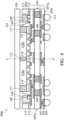
- Fig. 8 is a cross-sectional view of a semiconductor package structure 500c, in accordance with some embodiments of the invention.
- the semiconductor package structure 500c may include the same or similar portions as that of the semiconductor package structure 500b, and for the sake of simplicity, those portions will not be discussed in detail again.
- the semiconductor package structure 500c includes a substrate 101, a frame 113, semiconductor dies 115a, 115b, a heat sink 130, and a buffer layer 150.
- the buffer layer 150 is separated from the frame 113 and the semiconductor dies 115a, 115b, reducing the difficulty of forming the buffer layer 150.
- the frame 113 and the buffer layer 150 may not interfere the bonging between the semiconductor dies 115a, 115b and the heat sink 130.
- Fig. 9 is a cross-sectional view of a semiconductor package structure 500d, in accordance with some other examples not corresponding to the invention as defined in the claims but useful for the understanding thereof.
- the semiconductor package structure 500c may include the same or similar portions as that of the semiconductor package structure 500b, and for the sake of simplicity, those portions will not be discussed in detail again.
- the semiconductor package structure 500c includes a substrate 101, semiconductor dies 115a, 115b, a heat sink 130, and a buffer layer 150.
- the frame 113 is omitted and replaced by the buffer layer 150, such that the manufacturing process of the semiconductor package structure 500d may be simplified, reducing the required time and cost of the manufacturing process.
- the buffer layer 150 may provide sufficient support so as to reduce the warpage issue of the semiconductor package structure 500d.
- the heat sink 130 is disposed directly above the semiconductor dies 115a, 115b and the buffer layer 150.
- Fig. 10 is a cross-sectional view of a semiconductor package structure 500e, in accordance with some other examples not corresponding to the invention as defined in the claims but useful for the understanding thereof.
- the semiconductor package structure 500c may include the same or similar portions as that of the semiconductor package structure 500b, and for the sake of simplicity, those portions will not be discussed in detail again.
- the semiconductor package structure 500c includes a substrate 101, a frame 113, semiconductor dies 115a, 115b, a heat sink 130, and a buffer layer 150.
- the buffer layer 150 covers the upper surface of the frame 113.
- the frame 113 may not directly contact the heat sink 130 (namely, the frame 113 may be separated from the heat sink 130), and the buffer layer 150 contacts the heat sink 130 instead. Since the flatness of the surface formed by the buffer layer 150 may be higher than the flatness of the surface formed by the frame 113, a flatter interface between the buffer layer 150 and the heat sink 150. Accordingly, the contact between the semiconductor dies 115a, 115b and the heat sink 150 may be created, enhancing the thermal dissipation of the semiconductor dies 115a, 115b.
- the holes formed in the substrate are designed to release the stress in the substrate, especially the stress concentrated in the region below the interface between two semiconductor dies. Since the semiconductor package structure may be highly stressed due to the different coefficients of thermal expansion (CTEs) of the substrate and the semiconductor dies, the holes formed in the substrate can solve the warping or cracking problems caused by mismatched CTEs. As a result, the electrical connection within the semiconductor package structure may not be damaged, and the reliability and the lifespan of the semiconductor package structure may be increased.
- the buffer layer formed on the substrate may help to reduce warpage of the semiconductor package structure and/or enhance the thermal dissipation of the semiconductor dies.
- the semiconductor dies 115a and 115b may be formed in the same package, for example, the semiconductor dies 115a and 115b are disposed on a fan-out package interposer, the fan-out package interposer is a rewiring laminate structure.
- the semiconductor dies 115a and 115b could be disposed on a Chip-on-Wafer-on-Substrate (CoWoS) structure with a package interposer, the package interposer has multiple through silicon vias (TSVs) as interconnection between the semiconductore dies and the substrate 101.
- TSVs through silicon vias
- the semiconductor dies 115a and 115b may be formed in different packages, for example, the semiconductor die 115a could be a flip-chip (FC) package, while the semiconductor die 115b could be a fan-out structure.
- FC flip-chip
- the package construction may be varied to achieve different technical purposes.
- the semiconductor package structures in accordance with some embodiments of the disclosure can be used to form a three-dimensional (3D) package, a 2.5D package, a fan-out package, or another suitable package.
- the arrangements, the shapes, and the locations of the holes in the substrate can be adjusted according to the types of the application.
Landscapes
- Structures Or Materials For Encapsulating Or Coating Semiconductor Devices Or Solid State Devices (AREA)
- Cooling Or The Like Of Semiconductors Or Solid State Devices (AREA)
- Lead Frames For Integrated Circuits (AREA)
Claims (9)
- Halbleiter-Package-Struktur, aufweisend:ein Substrat (101);einen Halbleiter-Die (115a, 115b), der über dem Substrat (101) angeordnet ist;eine Unterfüllschicht (123) zwischen dem Halbleiter-Die (115a, 115b) und dem Substrat (101); undeinen Rahmen (113), der über dem Substrat (101) angeordnet ist, wobei der Rahmen (113) dem Halbleiter-Die (115a, 115b) benachbart ist und eine obere Oberfläche des Rahmens (113) niedriger als eine obere Oberfläche des Halbleiter-Die (115a, 115b) ist;aufweisend eine Pufferschicht (150), die über dem Substrat (101) angeordnet ist, wobei die Pufferschicht (150) zwischen dem Rahmen (113) und dem Halbleiter-Die (115a, 115b) angeordnet ist;ferner aufweisend einen Kühlkörper (130), der über dem Halbleiter-Die angeordnet ist, wobei der Kühlkörper (130) mit mindestens einem von dem Halbleiter-Die (115a, 115b) und der Pufferschicht (150) in Kontakt steht und von dem Rahmen (113) getrennt ist.
- Halbleiter-Package-Struktur nach Anspruch 1, wobei die Pufferschicht (150) die obere Oberfläche des Rahmens (113) bedeckt.
- Halbleiter-Package-Struktur nach Anspruch 1, wobei eine obere Oberfläche des Rahmens (113) mit einer oberen Oberfläche der Pufferschicht (150) niveaugleich ist.
- Halbleiter-Package-Struktur nach Anspruch 1, wobei die Pufferschicht (150) mit dem Rahmen (113) in Kontakt steht.
- Halbleiter-Package-Struktur nach einem der Ansprüche 1 bis 4, wobei sich in einer senkrecht zu der oberen Oberfläche des Halbleiter-Die (115a, 115b) verlaufenden Richtung betrachtet der Kühlkörper (130) mit dem Rahmen (113) und dem Halbleiter-Die (115a, 115b) überlappt.
- Halbleiter-Package-Struktur nach Anspruch 1, wobei eine obere Oberfläche der Pufferschicht (150) mit einer oberen Oberfläche des Halbleiter-Die (115a, 115b) niveaugleich ist.
- Halbleiter-Package-Struktur nach einem der Ansprüche 1 bis 3, wobei die Pufferschicht (150) von dem Rahmen (113) und dem Halbleiter-Die (115a, 115b) getrennt ist.
- Halbleiter-Package-Struktur nach Anspruch 1, wobei die Pufferschicht (150) eine obere Oberfläche des Rahmens (113) bedeckt.
- Halbleiter-Package-Struktur nach einem der vorhergehenden Ansprüche, ferner aufweisend eine passive Komponente (140), die auf dem Substrat (101) angeordnet ist, wobei die passive Komponente (140) von der Pufferschicht (150) umgeben ist.
Priority Applications (1)
| Application Number | Priority Date | Filing Date | Title |
|---|---|---|---|
| EP24194476.8A EP4439648A3 (de) | 2018-12-18 | 2019-12-04 | Halbleitergehäusestruktur |
Applications Claiming Priority (3)
| Application Number | Priority Date | Filing Date | Title |
|---|---|---|---|
| US201862781120P | 2018-12-18 | 2018-12-18 | |
| US201962848063P | 2019-05-15 | 2019-05-15 | |
| US16/702,104 US11264337B2 (en) | 2017-03-14 | 2019-12-03 | Semiconductor package structure |
Related Child Applications (2)
| Application Number | Title | Priority Date | Filing Date |
|---|---|---|---|
| EP24194476.8A Division EP4439648A3 (de) | 2018-12-18 | 2019-12-04 | Halbleitergehäusestruktur |
| EP24194476.8A Division-Into EP4439648A3 (de) | 2018-12-18 | 2019-12-04 | Halbleitergehäusestruktur |
Publications (2)
| Publication Number | Publication Date |
|---|---|
| EP3671831A1 EP3671831A1 (de) | 2020-06-24 |
| EP3671831B1 true EP3671831B1 (de) | 2024-09-18 |
Family
ID=68806566
Family Applications (2)
| Application Number | Title | Priority Date | Filing Date |
|---|---|---|---|
| EP19213567.1A Active EP3671831B1 (de) | 2018-12-18 | 2019-12-04 | Halbleiterpaketstruktur |
| EP24194476.8A Pending EP4439648A3 (de) | 2018-12-18 | 2019-12-04 | Halbleitergehäusestruktur |
Family Applications After (1)
| Application Number | Title | Priority Date | Filing Date |
|---|---|---|---|
| EP24194476.8A Pending EP4439648A3 (de) | 2018-12-18 | 2019-12-04 | Halbleitergehäusestruktur |
Country Status (3)
| Country | Link |
|---|---|
| EP (2) | EP3671831B1 (de) |
| CN (2) | CN111508946A (de) |
| TW (1) | TWI762841B (de) |
Families Citing this family (3)
| Publication number | Priority date | Publication date | Assignee | Title |
|---|---|---|---|---|
| US12394698B2 (en) * | 2021-07-23 | 2025-08-19 | Taiwan Semiconductor Manufacturing Company Limited | Underfill cushion films for packaging substrates and methods of forming the same |
| CN115732433A (zh) * | 2021-08-31 | 2023-03-03 | 日月光半导体制造股份有限公司 | 半导体封装结构 |
| US20240178159A1 (en) * | 2022-11-30 | 2024-05-30 | Mediatek Inc. | Coreless substrate package and fabrication method thereof |
Family Cites Families (16)
| Publication number | Priority date | Publication date | Assignee | Title |
|---|---|---|---|---|
| JP3437369B2 (ja) * | 1996-03-19 | 2003-08-18 | 松下電器産業株式会社 | チップキャリアおよびこれを用いた半導体装置 |
| JP3459804B2 (ja) * | 2000-02-28 | 2003-10-27 | Necエレクトロニクス株式会社 | 半導体装置 |
| JP4390541B2 (ja) * | 2003-02-03 | 2009-12-24 | Necエレクトロニクス株式会社 | 半導体装置及びその製造方法 |
| JP4714598B2 (ja) * | 2006-02-22 | 2011-06-29 | 富士通株式会社 | 半導体装置及びその製造方法 |
| US20080054490A1 (en) * | 2006-08-31 | 2008-03-06 | Ati Technologies Inc. | Flip-Chip Ball Grid Array Strip and Package |
| US7851906B2 (en) * | 2007-03-26 | 2010-12-14 | Endicott Interconnect Technologies, Inc. | Flexible circuit electronic package with standoffs |
| US8115303B2 (en) * | 2008-05-13 | 2012-02-14 | International Business Machines Corporation | Semiconductor package structures having liquid coolers integrated with first level chip package modules |
| US8247900B2 (en) * | 2009-12-29 | 2012-08-21 | Taiwan Semiconductor Manufacturing Company, Ltd. | Flip chip package having enhanced thermal and mechanical performance |
| KR101678539B1 (ko) * | 2010-07-21 | 2016-11-23 | 삼성전자 주식회사 | 적층 패키지, 반도체 패키지 및 적층 패키지의 제조 방법 |
| US8976529B2 (en) * | 2011-01-14 | 2015-03-10 | Taiwan Semiconductor Manufacturing Company, Ltd. | Lid design for reliability enhancement in flip chip package |
| US20120188721A1 (en) * | 2011-01-21 | 2012-07-26 | Nxp B.V. | Non-metal stiffener ring for fcbga |
| US9209048B2 (en) * | 2013-12-30 | 2015-12-08 | Taiwan Semiconductor Manufacturing Company, Ltd. | Two step molding grinding for packaging applications |
| US9892935B2 (en) * | 2015-05-28 | 2018-02-13 | International Business Machines Corporation | Limiting electronic package warpage with semiconductor chip lid and lid-ring |
| US9425171B1 (en) * | 2015-06-25 | 2016-08-23 | Nvidia Corporation | Removable substrate for controlling warpage of an integrated circuit package |
| JP2018113414A (ja) * | 2017-01-13 | 2018-07-19 | 新光電気工業株式会社 | 半導体装置とその製造方法 |
| US10784211B2 (en) * | 2017-03-14 | 2020-09-22 | Mediatek Inc. | Semiconductor package structure |
-
2019
- 2019-12-04 EP EP19213567.1A patent/EP3671831B1/de active Active
- 2019-12-04 EP EP24194476.8A patent/EP4439648A3/de active Pending
- 2019-12-10 CN CN201911261556.5A patent/CN111508946A/zh active Pending
- 2019-12-10 CN CN202211364860.4A patent/CN115799187A/zh active Pending
- 2019-12-11 TW TW108145283A patent/TWI762841B/zh active
Also Published As
| Publication number | Publication date |
|---|---|
| EP4439648A3 (de) | 2025-01-15 |
| TWI762841B (zh) | 2022-05-01 |
| CN111508946A (zh) | 2020-08-07 |
| CN115799187A (zh) | 2023-03-14 |
| TW202038410A (zh) | 2020-10-16 |
| EP4439648A2 (de) | 2024-10-02 |
| EP3671831A1 (de) | 2020-06-24 |
Similar Documents
| Publication | Publication Date | Title |
|---|---|---|
| US12525549B2 (en) | Semiconductor package structure | |
| US11862578B2 (en) | Semiconductor package structure | |
| US11942439B2 (en) | Semiconductor package structure | |
| EP3709344B1 (de) | Halbleitergehäusestruktur | |
| EP3754698B1 (de) | Halbleitergehäusestruktur | |
| US9966362B1 (en) | Integrated circuit package with inter-die thermal spreader layers | |
| US12002742B2 (en) | Semiconductor package structure | |
| TW201830616A (zh) | 具有高效率熱路徑及模製底部填充之堆置半導體晶粒組件 | |
| US12142598B2 (en) | Semiconductor package structure having an annular frame with truncated corners | |
| EP3671831A1 (de) | Halbleiterpaketstruktur | |
| TW202347674A (zh) | 晶片封裝結構及其形成方法 | |
| EP3624181B1 (de) | Halbleitergehäusestruktur mit einem rahmen mit abgeschnittenen ecken | |
| US12424531B2 (en) | Semiconductor package structure |
Legal Events
| Date | Code | Title | Description |
|---|---|---|---|
| PUAI | Public reference made under article 153(3) epc to a published international application that has entered the european phase |
Free format text: ORIGINAL CODE: 0009012 |
|
| STAA | Information on the status of an ep patent application or granted ep patent |
Free format text: STATUS: THE APPLICATION HAS BEEN PUBLISHED |
|
| AK | Designated contracting states |
Kind code of ref document: A1 Designated state(s): AL AT BE BG CH CY CZ DE DK EE ES FI FR GB GR HR HU IE IS IT LI LT LU LV MC MK MT NL NO PL PT RO RS SE SI SK SM TR |
|
| AX | Request for extension of the european patent |
Extension state: BA ME |
|
| STAA | Information on the status of an ep patent application or granted ep patent |
Free format text: STATUS: REQUEST FOR EXAMINATION WAS MADE |
|
| 17P | Request for examination filed |
Effective date: 20201120 |
|
| RBV | Designated contracting states (corrected) |
Designated state(s): AL AT BE BG CH CY CZ DE DK EE ES FI FR GB GR HR HU IE IS IT LI LT LU LV MC MK MT NL NO PL PT RO RS SE SI SK SM TR |
|
| STAA | Information on the status of an ep patent application or granted ep patent |
Free format text: STATUS: EXAMINATION IS IN PROGRESS |
|
| 17Q | First examination report despatched |
Effective date: 20211220 |
|
| P01 | Opt-out of the competence of the unified patent court (upc) registered |
Effective date: 20230607 |
|
| GRAP | Despatch of communication of intention to grant a patent |
Free format text: ORIGINAL CODE: EPIDOSNIGR1 |
|
| STAA | Information on the status of an ep patent application or granted ep patent |
Free format text: STATUS: GRANT OF PATENT IS INTENDED |
|
| INTG | Intention to grant announced |
Effective date: 20240415 |
|
| RAP3 | Party data changed (applicant data changed or rights of an application transferred) |
Owner name: MEDIATEK INC. |
|
| RIN1 | Information on inventor provided before grant (corrected) |
Inventor name: LIN, YI-JOU Inventor name: PENG, I-HSUAN Inventor name: LIN, TZU-HUNG Inventor name: CHANG, CHIA-CHENG |
|
| GRAS | Grant fee paid |
Free format text: ORIGINAL CODE: EPIDOSNIGR3 |
|
| GRAA | (expected) grant |
Free format text: ORIGINAL CODE: 0009210 |
|
| STAA | Information on the status of an ep patent application or granted ep patent |
Free format text: STATUS: THE PATENT HAS BEEN GRANTED |
|
| AK | Designated contracting states |
Kind code of ref document: B1 Designated state(s): AL AT BE BG CH CY CZ DE DK EE ES FI FR GB GR HR HU IE IS IT LI LT LU LV MC MK MT NL NO PL PT RO RS SE SI SK SM TR |
|
| REG | Reference to a national code |
Ref country code: GB Ref legal event code: FG4D |
|
| REG | Reference to a national code |
Ref country code: CH Ref legal event code: EP |
|
| REG | Reference to a national code |
Ref country code: DE Ref legal event code: R096 Ref document number: 602019059019 Country of ref document: DE |
|
| REG | Reference to a national code |
Ref country code: IE Ref legal event code: FG4D |
|
| REG | Reference to a national code |
Ref country code: LT Ref legal event code: MG9D |
|
| PG25 | Lapsed in a contracting state [announced via postgrant information from national office to epo] |
Ref country code: NO Free format text: LAPSE BECAUSE OF FAILURE TO SUBMIT A TRANSLATION OF THE DESCRIPTION OR TO PAY THE FEE WITHIN THE PRESCRIBED TIME-LIMIT Effective date: 20241218 |
|
| PG25 | Lapsed in a contracting state [announced via postgrant information from national office to epo] |
Ref country code: GR Free format text: LAPSE BECAUSE OF FAILURE TO SUBMIT A TRANSLATION OF THE DESCRIPTION OR TO PAY THE FEE WITHIN THE PRESCRIBED TIME-LIMIT Effective date: 20241219 Ref country code: FI Free format text: LAPSE BECAUSE OF FAILURE TO SUBMIT A TRANSLATION OF THE DESCRIPTION OR TO PAY THE FEE WITHIN THE PRESCRIBED TIME-LIMIT Effective date: 20240918 |
|
| PG25 | Lapsed in a contracting state [announced via postgrant information from national office to epo] |
Ref country code: BG Free format text: LAPSE BECAUSE OF FAILURE TO SUBMIT A TRANSLATION OF THE DESCRIPTION OR TO PAY THE FEE WITHIN THE PRESCRIBED TIME-LIMIT Effective date: 20240918 |
|
| PG25 | Lapsed in a contracting state [announced via postgrant information from national office to epo] |
Ref country code: LV Free format text: LAPSE BECAUSE OF FAILURE TO SUBMIT A TRANSLATION OF THE DESCRIPTION OR TO PAY THE FEE WITHIN THE PRESCRIBED TIME-LIMIT Effective date: 20240918 |
|
| PG25 | Lapsed in a contracting state [announced via postgrant information from national office to epo] |
Ref country code: HR Free format text: LAPSE BECAUSE OF FAILURE TO SUBMIT A TRANSLATION OF THE DESCRIPTION OR TO PAY THE FEE WITHIN THE PRESCRIBED TIME-LIMIT Effective date: 20240918 |
|
| REG | Reference to a national code |
Ref country code: NL Ref legal event code: MP Effective date: 20240918 |
|
| PG25 | Lapsed in a contracting state [announced via postgrant information from national office to epo] |
Ref country code: RS Free format text: LAPSE BECAUSE OF FAILURE TO SUBMIT A TRANSLATION OF THE DESCRIPTION OR TO PAY THE FEE WITHIN THE PRESCRIBED TIME-LIMIT Effective date: 20241218 |
|
| PG25 | Lapsed in a contracting state [announced via postgrant information from national office to epo] |
Ref country code: RS Free format text: LAPSE BECAUSE OF FAILURE TO SUBMIT A TRANSLATION OF THE DESCRIPTION OR TO PAY THE FEE WITHIN THE PRESCRIBED TIME-LIMIT Effective date: 20241218 Ref country code: NO Free format text: LAPSE BECAUSE OF FAILURE TO SUBMIT A TRANSLATION OF THE DESCRIPTION OR TO PAY THE FEE WITHIN THE PRESCRIBED TIME-LIMIT Effective date: 20241218 Ref country code: LV Free format text: LAPSE BECAUSE OF FAILURE TO SUBMIT A TRANSLATION OF THE DESCRIPTION OR TO PAY THE FEE WITHIN THE PRESCRIBED TIME-LIMIT Effective date: 20240918 Ref country code: HR Free format text: LAPSE BECAUSE OF FAILURE TO SUBMIT A TRANSLATION OF THE DESCRIPTION OR TO PAY THE FEE WITHIN THE PRESCRIBED TIME-LIMIT Effective date: 20240918 Ref country code: GR Free format text: LAPSE BECAUSE OF FAILURE TO SUBMIT A TRANSLATION OF THE DESCRIPTION OR TO PAY THE FEE WITHIN THE PRESCRIBED TIME-LIMIT Effective date: 20241219 Ref country code: FI Free format text: LAPSE BECAUSE OF FAILURE TO SUBMIT A TRANSLATION OF THE DESCRIPTION OR TO PAY THE FEE WITHIN THE PRESCRIBED TIME-LIMIT Effective date: 20240918 Ref country code: BG Free format text: LAPSE BECAUSE OF FAILURE TO SUBMIT A TRANSLATION OF THE DESCRIPTION OR TO PAY THE FEE WITHIN THE PRESCRIBED TIME-LIMIT Effective date: 20240918 |
|
| REG | Reference to a national code |
Ref country code: AT Ref legal event code: MK05 Ref document number: 1725441 Country of ref document: AT Kind code of ref document: T Effective date: 20240918 |
|
| PG25 | Lapsed in a contracting state [announced via postgrant information from national office to epo] |
Ref country code: NL Free format text: LAPSE BECAUSE OF FAILURE TO SUBMIT A TRANSLATION OF THE DESCRIPTION OR TO PAY THE FEE WITHIN THE PRESCRIBED TIME-LIMIT Effective date: 20240918 |
|
| PG25 | Lapsed in a contracting state [announced via postgrant information from national office to epo] |
Ref country code: IS Free format text: LAPSE BECAUSE OF FAILURE TO SUBMIT A TRANSLATION OF THE DESCRIPTION OR TO PAY THE FEE WITHIN THE PRESCRIBED TIME-LIMIT Effective date: 20250118 Ref country code: PT Free format text: LAPSE BECAUSE OF FAILURE TO SUBMIT A TRANSLATION OF THE DESCRIPTION OR TO PAY THE FEE WITHIN THE PRESCRIBED TIME-LIMIT Effective date: 20250120 |
|
| PG25 | Lapsed in a contracting state [announced via postgrant information from national office to epo] |
Ref country code: RO Free format text: LAPSE BECAUSE OF FAILURE TO SUBMIT A TRANSLATION OF THE DESCRIPTION OR TO PAY THE FEE WITHIN THE PRESCRIBED TIME-LIMIT Effective date: 20240918 Ref country code: SM Free format text: LAPSE BECAUSE OF FAILURE TO SUBMIT A TRANSLATION OF THE DESCRIPTION OR TO PAY THE FEE WITHIN THE PRESCRIBED TIME-LIMIT Effective date: 20240918 |
|
| PG25 | Lapsed in a contracting state [announced via postgrant information from national office to epo] |
Ref country code: ES Free format text: LAPSE BECAUSE OF FAILURE TO SUBMIT A TRANSLATION OF THE DESCRIPTION OR TO PAY THE FEE WITHIN THE PRESCRIBED TIME-LIMIT Effective date: 20240918 |
|
| PG25 | Lapsed in a contracting state [announced via postgrant information from national office to epo] |
Ref country code: AT Free format text: LAPSE BECAUSE OF FAILURE TO SUBMIT A TRANSLATION OF THE DESCRIPTION OR TO PAY THE FEE WITHIN THE PRESCRIBED TIME-LIMIT Effective date: 20240918 Ref country code: EE Free format text: LAPSE BECAUSE OF FAILURE TO SUBMIT A TRANSLATION OF THE DESCRIPTION OR TO PAY THE FEE WITHIN THE PRESCRIBED TIME-LIMIT Effective date: 20240918 |
|
| PG25 | Lapsed in a contracting state [announced via postgrant information from national office to epo] |
Ref country code: PL Free format text: LAPSE BECAUSE OF FAILURE TO SUBMIT A TRANSLATION OF THE DESCRIPTION OR TO PAY THE FEE WITHIN THE PRESCRIBED TIME-LIMIT Effective date: 20240918 Ref country code: CZ Free format text: LAPSE BECAUSE OF FAILURE TO SUBMIT A TRANSLATION OF THE DESCRIPTION OR TO PAY THE FEE WITHIN THE PRESCRIBED TIME-LIMIT Effective date: 20240918 |
|
| PG25 | Lapsed in a contracting state [announced via postgrant information from national office to epo] |
Ref country code: SK Free format text: LAPSE BECAUSE OF FAILURE TO SUBMIT A TRANSLATION OF THE DESCRIPTION OR TO PAY THE FEE WITHIN THE PRESCRIBED TIME-LIMIT Effective date: 20240918 Ref country code: IT Free format text: LAPSE BECAUSE OF FAILURE TO SUBMIT A TRANSLATION OF THE DESCRIPTION OR TO PAY THE FEE WITHIN THE PRESCRIBED TIME-LIMIT Effective date: 20240918 |
|
| REG | Reference to a national code |
Ref country code: DE Ref legal event code: R097 Ref document number: 602019059019 Country of ref document: DE |
|
| PG25 | Lapsed in a contracting state [announced via postgrant information from national office to epo] |
Ref country code: MC Free format text: LAPSE BECAUSE OF FAILURE TO SUBMIT A TRANSLATION OF THE DESCRIPTION OR TO PAY THE FEE WITHIN THE PRESCRIBED TIME-LIMIT Effective date: 20240918 |
|
| PG25 | Lapsed in a contracting state [announced via postgrant information from national office to epo] |
Ref country code: DK Free format text: LAPSE BECAUSE OF FAILURE TO SUBMIT A TRANSLATION OF THE DESCRIPTION OR TO PAY THE FEE WITHIN THE PRESCRIBED TIME-LIMIT Effective date: 20240918 |
|
| PLBE | No opposition filed within time limit |
Free format text: ORIGINAL CODE: 0009261 |
|
| STAA | Information on the status of an ep patent application or granted ep patent |
Free format text: STATUS: NO OPPOSITION FILED WITHIN TIME LIMIT |
|
| REG | Reference to a national code |
Ref country code: CH Ref legal event code: PL |
|
| PG25 | Lapsed in a contracting state [announced via postgrant information from national office to epo] |
Ref country code: LU Free format text: LAPSE BECAUSE OF NON-PAYMENT OF DUE FEES Effective date: 20241204 |
|
| 26N | No opposition filed |
Effective date: 20250619 |
|
| PG25 | Lapsed in a contracting state [announced via postgrant information from national office to epo] |
Ref country code: SE Free format text: LAPSE BECAUSE OF FAILURE TO SUBMIT A TRANSLATION OF THE DESCRIPTION OR TO PAY THE FEE WITHIN THE PRESCRIBED TIME-LIMIT Effective date: 20240918 |
|
| REG | Reference to a national code |
Ref country code: BE Ref legal event code: MM Effective date: 20241231 |
|
| PG25 | Lapsed in a contracting state [announced via postgrant information from national office to epo] |
Ref country code: BE Free format text: LAPSE BECAUSE OF NON-PAYMENT OF DUE FEES Effective date: 20241231 |
|
| PGFP | Annual fee paid to national office [announced via postgrant information from national office to epo] |
Ref country code: FR Payment date: 20250930 Year of fee payment: 7 |
|
| PG25 | Lapsed in a contracting state [announced via postgrant information from national office to epo] |
Ref country code: CH Free format text: LAPSE BECAUSE OF NON-PAYMENT OF DUE FEES Effective date: 20241231 |
|
| PG25 | Lapsed in a contracting state [announced via postgrant information from national office to epo] |
Ref country code: IE Free format text: LAPSE BECAUSE OF NON-PAYMENT OF DUE FEES Effective date: 20241204 |
|
| REG | Reference to a national code |
Ref country code: DE Ref legal event code: R079 Ref document number: 602019059019 Country of ref document: DE Free format text: PREVIOUS MAIN CLASS: H01L0023498000 Ipc: H10W0070620000 |
|
| PGFP | Annual fee paid to national office [announced via postgrant information from national office to epo] |
Ref country code: DE Payment date: 20250930 Year of fee payment: 7 |
|
| PGFP | Annual fee paid to national office [announced via postgrant information from national office to epo] |
Ref country code: GB Payment date: 20251001 Year of fee payment: 7 |
|
| PG25 | Lapsed in a contracting state [announced via postgrant information from national office to epo] |
Ref country code: CY Free format text: LAPSE BECAUSE OF FAILURE TO SUBMIT A TRANSLATION OF THE DESCRIPTION OR TO PAY THE FEE WITHIN THE PRESCRIBED TIME-LIMIT; INVALID AB INITIO Effective date: 20191204 |