EP3671855A1 - Module d'affichage de pixels et plaque de masque pour sa fabrication - Google Patents
Module d'affichage de pixels et plaque de masque pour sa fabrication Download PDFInfo
- Publication number
- EP3671855A1 EP3671855A1 EP19825098.7A EP19825098A EP3671855A1 EP 3671855 A1 EP3671855 A1 EP 3671855A1 EP 19825098 A EP19825098 A EP 19825098A EP 3671855 A1 EP3671855 A1 EP 3671855A1
- Authority
- EP
- European Patent Office
- Prior art keywords
- pixel
- pixel unit
- sub
- pixels
- color light
- Prior art date
- Legal status (The legal status is an assumption and is not a legal conclusion. Google has not performed a legal analysis and makes no representation as to the accuracy of the status listed.)
- Pending
Links
Images

Classifications
-
- C—CHEMISTRY; METALLURGY
- C23—COATING METALLIC MATERIAL; COATING MATERIAL WITH METALLIC MATERIAL; CHEMICAL SURFACE TREATMENT; DIFFUSION TREATMENT OF METALLIC MATERIAL; COATING BY VACUUM EVAPORATION, BY SPUTTERING, BY ION IMPLANTATION OR BY CHEMICAL VAPOUR DEPOSITION, IN GENERAL; INHIBITING CORROSION OF METALLIC MATERIAL OR INCRUSTATION IN GENERAL
- C23C—COATING METALLIC MATERIAL; COATING MATERIAL WITH METALLIC MATERIAL; SURFACE TREATMENT OF METALLIC MATERIAL BY DIFFUSION INTO THE SURFACE, BY CHEMICAL CONVERSION OR SUBSTITUTION; COATING BY VACUUM EVAPORATION, BY SPUTTERING, BY ION IMPLANTATION OR BY CHEMICAL VAPOUR DEPOSITION, IN GENERAL
- C23C14/00—Coating by vacuum evaporation, by sputtering or by ion implantation of the coating forming material
- C23C14/04—Coating on selected surface areas, e.g. using masks
- C23C14/042—Coating on selected surface areas, e.g. using masks using masks
-
- H—ELECTRICITY
- H10—SEMICONDUCTOR DEVICES; ELECTRIC SOLID-STATE DEVICES NOT OTHERWISE PROVIDED FOR
- H10K—ORGANIC ELECTRIC SOLID-STATE DEVICES
- H10K59/00—Integrated devices, or assemblies of multiple devices, comprising at least one organic light-emitting element covered by group H10K50/00
- H10K59/30—Devices specially adapted for multicolour light emission
- H10K59/35—Devices specially adapted for multicolour light emission comprising red-green-blue [RGB] subpixels
- H10K59/353—Devices specially adapted for multicolour light emission comprising red-green-blue [RGB] subpixels characterised by the geometrical arrangement of the RGB subpixels
-
- H—ELECTRICITY
- H10—SEMICONDUCTOR DEVICES; ELECTRIC SOLID-STATE DEVICES NOT OTHERWISE PROVIDED FOR
- H10K—ORGANIC ELECTRIC SOLID-STATE DEVICES
- H10K71/00—Manufacture or treatment specially adapted for the organic devices covered by this subclass
-
- H—ELECTRICITY
- H10—SEMICONDUCTOR DEVICES; ELECTRIC SOLID-STATE DEVICES NOT OTHERWISE PROVIDED FOR
- H10K—ORGANIC ELECTRIC SOLID-STATE DEVICES
- H10K71/00—Manufacture or treatment specially adapted for the organic devices covered by this subclass
- H10K71/10—Deposition of organic active material
- H10K71/16—Deposition of organic active material using physical vapour deposition [PVD], e.g. vacuum deposition or sputtering
- H10K71/166—Deposition of organic active material using physical vapour deposition [PVD], e.g. vacuum deposition or sputtering using selective deposition, e.g. using a mask
Definitions
- Embodiments of the present application relate to the field of display technology, and particularly to a pixel display module and a mask for manufacturing the pixel display module.
- RGB the most common application of three-color.
- a change of color can be realized through a change of three color channels of red R, green G and blue B and their superposition, which is one of color systems used widely.
- the performance of the display is usually represented by a display resolution.
- the display resolution is a quantity of individual pixels that can emit a light in each dimension (i.e. 1920 ⁇ 1080), or the performance of the display is usually represented by a display density that is a relative quantity of pixels per inch (aka pixels per inch PPI).
- an organic light-emitting layer of an OLED is manufactured by an evaporation technique using a fine metal mask (FMM).
- FMM fine metal mask
- technology precision of composing a picture on organic materials is high, and so the minimum size of each layer is limited.
- a sufficient space must be maintained between adjacent pixels to avoid overlapping of adjacent organic light-emitting layers. Therefore, due to the limitations of the fine metal mask and the evaporation process itself, for example, a mask opening cannot be made smaller.
- the high PPI can be achieved through an arrangement of pixels, the evaporation process using two or more masks increases the cost and process time.
- embodiments of the present application provide a pixel display module and a mask for manufacturing the pixel display module in order to solve the problem that it is difficult to manufacture display devices with high PPI and uniformity.
- An aspect of the present application provides a pixel display module, including: a plurality of array-distributed pixel unit groups. Each pixel unit group includes four array-distributed sub-pixels.
- Two sub-pixels located on a diagonal of each pixel unit group emit a same first color light, and two sub-pixels located on another diagonal of each pixel unit group respectively emit a second color light and a third color light.
- Two pixel unit groups adjacent in a first direction are misaligned along a second direction, and the second direction is perpendicular to the first direction.
- An aspect of the present application provides a mask for manufacturing the pixel display module, including: a plurality of open areas, wherein at least one open area corresponds to two sub-pixels which are respectively belonging to the two adjacent pixel unit groups, are adjacent to each other, are located in a same row or in a same column and emit the same color light.
- the embodiments of the present application provide a pixel display module, and the pixel display module includes a plurality of array-distributed pixel unit groups.
- Each pixel unit group includes four array-distributed sub-pixels. Two sub-pixels located on a diagonal of each the pixel unit groups emit a same first color light, and two sub-pixels located on another diagonal of each pixel unit group respectively emit a second color light and a third color light. It is ensured that two sub-pixels that emit a same color light are misaligned in position, and the display effect is more uniform.
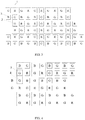
- FIG. 1 is a schematic structural diagram of a pixel display module according to an embodiment of the present application.
- the pixel display module includes a plurality of array-distributed pixel unit groups 1.
- Each pixel unit group 1 includes four array-distributed sub-pixels.
- a sub-pixel 2 and a sub-pixel 3 located on a diagonal of a pixel unit group 1 emit a same first color light
- a sub-pixel 4 and a sub-pixel 5 located on another diagonal of the pixel unit group 1 respectively emit a second color light and a third color light.
- the diagonal having sub-pixels that emit the same color light of the pixel unit group may be selected according to actual needs and manufacture process.
- the sub-pixel 4 and the sub-pixel 5 located on a diagonal of the pixel unit group 1 emit the same first color light
- the sub-pixel 2 and the sub-pixel 3 located on the another diagonal of the pixel unit group 1 respectively emit the second color light and the third color light.
- the embodiments of the present application provide the pixel display module including the plurality of array-distributed pixel unit groups 1.
- Each pixel unit group 1 includes four array-distributed sub-pixels. Two sub-pixels located on a diagonal of each pixel unit group emit the same first color light, and two sub-pixels located on another diagonal of each pixel unit group respectively emit the second color light and the third color light. It is ensured that two sub-pixels that emit the same color light are misaligned in position, and the uniformity of the display can be improved.
- An embodiment of the present application provides a pixel display module.
- Two pixel unit groups adjacent in a first direction are misaligned along a second direction, and the second direction is perpendicular to the first direction.
- the first direction is a column direction
- the second direction is a row direction correspondingly.
- Two pixel unit groups 1 adjacent in the column direction are misaligned along the row direction, which may be misaligned to the right or left.
- a misaligned distance is less than a distance of one sub-pixel in the row direction, i.e., in the two pixel unit groups adjacent in the column direction, one sub-pixel in a lower pixel unit group 1 is located between two pixels of the above pixel unit group 1 in the column direction.
- a direction of moving along the left and right reading direction is defined as the row direction of the pixel display module
- a direction of moving along the up and down reading direction is defined as the column direction of the pixel display module.
- the misaligned distance along the row direction of the two pixel unit groups 1 that are adjacent in the column direction may be selected according to the actual pixel requirements and process requirements.
- the misaligned distance may be less than the dimension of one sub-pixel in the row direction, or the misaligned distance may be more than the dimension of one sub-pixel in the row direction, or the misaligned distance may be equal to the dimension of one sub-pixel, which is not limited in the embodiments of the present application.
- the first direction is the row direction
- the second direction is the column direction correspondingly.
- Two pixel unit groups 1 adjacent are misaligned a distance along the column direction and the distance may be selected according to the actual pixel requirements and process requirements, which is not limited in the embodiments of the present application.
- Two pixel unit groups 1 adjacent are misaligned, so that the sub-pixels emitting the first color light, the sub-pixels emitting the second color light, and the sub-pixels emitting the third color light are uniformly distributed in the column direction or the row direction.
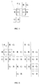
- a pixel display module is provided by an embodiment of the present application, as shown in FIG. 3 .
- a first direction is a column direction
- a second direction is a row direction correspondingly.
- Two pixel unit groups adjacent to each other in the column direction are misaligned to the right by a distance of one sub-pixel along the row direction. That is to say, in the column direction, a first sub-pixel 2 of a first row in a first pixel unit group 1 located in a lower row is located directly below a second sub-pixel 3 of a second row in a first pixel unit group 1 located in an upper row, and the first sub-pixel 2 and the second sub-pixel 3 emit a same color light.
- the first sub-pixel 2 and the second sub-pixel 3 emit a first color light, i.e., two sub-pixels on a diagonal of the pixel unit group 1 emit a same color light. In an embodiment of the present application, two sub-pixels on a diagonal of the pixel unit group 1 emit green light.
- two pixel unit groups adjacent in the column direction are misaligned a distance of one sub-pixel along the row direction.
- Two sub-pixels which are adjacent to each other in the column direction and are respectively belonging to the two adjacent pixel unit groups, emit a same color light.
- the two sub-pixels that emit the same color light can share one opening on the mask to increase the aperture ratio of the display device. Under the process conditions, a pixel unit of a smaller size can be fabricated; thereby the PPI of the display device is increased.
- two pixel unit groups adjacent in the column direction are misaligned in the row direction with a distance of one sub-pixel along the row direction.
- the lower pixel unit group is misaligned to the left or the right relative to the upper pixel unit group may be selected according to the arrangement of sub-pixels in the pixel unit groups.
- the group of pixel units in the next row is misaligned a distance of one sub-pixel along the row direction to the left along the row direction.
- a second sub-pixel 4 of a first row in a first pixel unit group 1 located in a lower row is located directly below a first sub-pixel 5 of a second row in the first pixel unit group 1 located in an upper row, which is not limited in the embodiments of the present application.
- the second direction is a column direction
- the first direction is a row direction
- the second direction is a column direction
- two adjacent pixel unit groups 1 in the column direction can be misaligned a distance of one sub-pixel along the row direction
- two adjacent pixel unit groups 1 in the row direction can be misaligned a distance of one sub-pixel distance along the column direction.
- two pixel unit groups 1 adjacent in the row direction are misaligned a distance of one sub-pixel dimension along the column direction, i.
- a first sub-pixel 5 of a second row of a right first pixel unit group is located on the right side or the left side of a second sub-pixel 4 of a first row of a left first pixel unit group, and the first sub-pixel 5 and the second sub-pixel 4 emit a same color light.
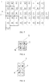
- a schematic structural diagram of the pixel display module composed of the array-distributed pixel unit groups is shown in FIG. 6 .
- the distance, mentioned above, of a sub-pixel refers to a dimension of a sub-pixel in a direction in which two adjacent pixel unit groups are misaligned with each other. That is to say, as shown in FIG. 7 , when two adjacent pixel unit groups are misaligned with each other along the row direction, the distance of one sub-pixel D is equal to the dimension of a sub-pixel itself in the row direction plus a dimension of a right spacing connected to the sub-pixel in the row direction, and plus a dimension of a left spacing connected to the sub-pixel in the row direction.
- the embodiments of the present application provide a pixel display module, and the pixel display module includes a plurality of array-distributed pixel unit groups.
- Each pixel unit group includes four array-distributed sub-pixels. Two sub-pixels located on a diagonal of each pixel unit group emit a same first color light, and two sub-pixels located on another diagonal of each pixel unit group respectively emit a second color light and a third color light.
- the first color light is green light
- the second color light and the third color light are respectively red light and blue light.
- the colors of the first color light, the second color light and the third color light can be selected according to actual need.
- the first color light may be blue light
- the second color light and the third color light may be respectively red light and green light.
- the first color light may be red light
- the second color light and the third color light may be respectively green light and blue light.
- a shape of the pixel unit group is a rectangle, so that the entire pixel is arranged in a rectangular array, which reduces the difficulty of mounting the mask.
- a length and a width of the rectangle may be selected according to actual need and process.
- a shape of the pixel unit group is a square, which is not limited in the embodiments of the present application.
- shapes of four sub-pixels in the pixel unit group are designed according to the actual application scenario.
- the shapes of four sub-pixels in the pixel unit group may all be square, or may all be rectangular, may partially be rectangular and partially be square, as shown in FIG. 7 .
- the shapes of the four sub-pixels in the pixel unit group are not limited in the embodiments of the present application.
- the embodiments of the present application provide a pixel display module, and the pixel display module includes a plurality of array-distributed pixel unit groups 1.
- Each pixel unit group 1 comprises a first pixel unit 6 and a second pixel unit 7.
- the first pixel unit 6 or the second pixel unit 7 is composed of three sub-pixels emitting different color lights.
- the first pixel unit 6 and the second pixel unit 7 share two sub-pixels, which respectively emit a second color light and a third color light and are located on a diagonal of the pixel unit group 1 .
- the first pixel unit 6 and the second pixel unit 7 share the two sub-pixels, which emit the different light and said two sub-pixels are located on a diagonal of the pixel unit group; and two sub-pixels, not shared by the first pixel unit 6 and the second pixel unit 7, emit a same color light.
- the display uniformity of the pixel unit group 1 is improved.
- a distance between two sub-pixels in the column direction is twice a distance between two sub-pixels in the row direction.
- the distance between two sub-pixels refers to a distance between the centers of two sub-pixels.
- the distance between two sub-pixels of the pixel unit group in the column direction is twice the distance between two sub-pixels in the row direction.
- the display shapes of the first pixel unit 6 and the second pixel unit 7 are all square, so that the displaying signal and displaying proportion of the display device will not be interfered.
- the shapes of the four sub-pixels in each pixel unit group 1 are rectangular as shown in FIG. 9 .
- a shape of each sub-pixel of the four sub-pixels in each pixel unit group 1 may be selected according to a specific application scenario, for example, the shape may be a square, or may be a rectangle the four corners of which are rounded.
- the shape of the sub-pixel is not limited in the embodiments of the application.
- the embodiments of the present application provide a mask for manufacturing the pixel display module.
- the mask includes a plurality of open areas, and at least one open area corresponds to two sub-pixels, which are respectively belong to the two adjacent pixel unit groups, are located in a same row or in a same column and emit the same color light. Since sub-pixels emitting different colors in a pixel structure are made by different evaporation processes, the masks corresponding to the sub-pixels emitting different colors are also different.
- An opening on the mask for manufacturing the pixel display module according to the embodiments of the application corresponds to two adjacent sub-pixels, which emit a same color light and respectively belong to two adjacent pixel unit groups.
Landscapes
- Chemical & Material Sciences (AREA)
- Engineering & Computer Science (AREA)
- Chemical Kinetics & Catalysis (AREA)
- Materials Engineering (AREA)
- Mechanical Engineering (AREA)
- Metallurgy (AREA)
- Organic Chemistry (AREA)
- Manufacturing & Machinery (AREA)
- Devices For Indicating Variable Information By Combining Individual Elements (AREA)
- Electroluminescent Light Sources (AREA)
- Physical Vapour Deposition (AREA)
Applications Claiming Priority (2)
| Application Number | Priority Date | Filing Date | Title |
|---|---|---|---|
| CN201810679353.7A CN108598141B (zh) | 2018-06-27 | 2018-06-27 | 一种像素显示模组以及制作像素显示模组的掩膜板 |
| PCT/CN2019/088556 WO2020001214A1 (fr) | 2018-06-27 | 2019-05-27 | Module d'affichage de pixels et plaque de masque pour sa fabrication |
Publications (2)
| Publication Number | Publication Date |
|---|---|
| EP3671855A1 true EP3671855A1 (fr) | 2020-06-24 |
| EP3671855A4 EP3671855A4 (fr) | 2020-12-30 |
Family
ID=63634106
Family Applications (1)
| Application Number | Title | Priority Date | Filing Date |
|---|---|---|---|
| EP19825098.7A Pending EP3671855A4 (fr) | 2018-06-27 | 2019-05-27 | Module d'affichage de pixels et plaque de masque pour sa fabrication |
Country Status (6)
| Country | Link |
|---|---|
| US (1) | US11069749B2 (fr) |
| EP (1) | EP3671855A4 (fr) |
| JP (1) | JP7043592B2 (fr) |
| KR (1) | KR102455818B1 (fr) |
| CN (1) | CN108598141B (fr) |
| WO (1) | WO2020001214A1 (fr) |
Families Citing this family (8)
| Publication number | Priority date | Publication date | Assignee | Title |
|---|---|---|---|---|
| CN108598141B (zh) | 2018-06-27 | 2020-12-11 | 昆山国显光电有限公司 | 一种像素显示模组以及制作像素显示模组的掩膜板 |
| CN110993665B (zh) * | 2019-12-06 | 2022-04-29 | 云谷(固安)科技有限公司 | 一种像素排列结构及显示面板 |
| CN111509023B (zh) * | 2020-05-06 | 2022-05-20 | 京东方科技集团股份有限公司 | 显示面板和显示装置 |
| CN111383551A (zh) * | 2020-05-09 | 2020-07-07 | 广州视源电子科技股份有限公司 | 一种led灯珠及led显示屏 |
| CN114649313B (zh) * | 2020-12-18 | 2025-09-09 | 富泰华工业(深圳)有限公司 | 显示装置的制造方法 |
| CN116897607A (zh) * | 2021-05-31 | 2023-10-17 | 京东方科技集团股份有限公司 | 显示基板以及显示装置 |
| KR20240121381A (ko) * | 2023-02-01 | 2024-08-09 | 삼성디스플레이 주식회사 | 발광 표시 장치 |
| CN116682332B (zh) * | 2023-08-02 | 2023-11-14 | 长春希达电子技术有限公司 | 一种led亚像素排列结构及模组 |
Family Cites Families (27)
| Publication number | Priority date | Publication date | Assignee | Title |
|---|---|---|---|---|
| TWI227340B (en) * | 2002-02-25 | 2005-02-01 | Himax Tech Inc | Color filter and liquid crystal display |
| JP2005208522A (ja) | 2004-01-26 | 2005-08-04 | Sharp Corp | 表示装置 |
| JP4260754B2 (ja) | 2005-01-31 | 2009-04-30 | 富士通株式会社 | デイスク装置のシークエラーリトライ方法及びデイスク装置 |
| US20060192433A1 (en) | 2005-02-28 | 2006-08-31 | Fuglevand William A | Uninterruptible power supply and method for supplying uninterruptible power to a load |
| TWI342721B (en) | 2006-05-18 | 2011-05-21 | Au Optronics Corp | Shadow mask and evaporation device incorporating the same and method for manufacturing organic light emitting diode panel incoporating the same |
| WO2008093862A1 (fr) * | 2007-02-02 | 2008-08-07 | Canon Kabushiki Kaisha | Afficheur et son procédé de production |
| JP4721460B2 (ja) * | 2007-02-02 | 2011-07-13 | キヤノン株式会社 | 表示装置及びその製造方法 |
| KR101663564B1 (ko) * | 2010-03-26 | 2016-10-17 | 엘지디스플레이 주식회사 | 유기전계발광소자 및 이의 제조방법 |
| TW201323926A (zh) * | 2011-12-07 | 2013-06-16 | Chunghwa Picture Tubes Ltd | 立體影像顯示裝置 |
| CN103123927B (zh) * | 2013-01-24 | 2015-05-06 | 昆山维信诺显示技术有限公司 | 用于oled显示屏的像素结构及其金属掩膜板 |
| KR102136584B1 (ko) * | 2013-12-27 | 2020-08-14 | 삼성디스플레이 주식회사 | 표시장치 |
| CN105097865A (zh) * | 2014-04-23 | 2015-11-25 | 上海和辉光电有限公司 | 应用于主动式有机发光二极管amoled显示器的像素排列结构 |
| JP2016075868A (ja) * | 2014-10-09 | 2016-05-12 | Nltテクノロジー株式会社 | 画素アレイ及び電気光学装置並びに電気機器並びに画素レンダリング方法 |
| CN106486513B (zh) * | 2015-08-31 | 2023-09-29 | 昆山国显光电有限公司 | 像素结构以及oled显示面板 |
| CN105242436B (zh) | 2015-11-06 | 2018-08-17 | 上海天马有机发光显示技术有限公司 | 一种阵列基板、显示面板及显示装置 |
| CN205231067U (zh) | 2015-12-24 | 2016-05-11 | 昆山国显光电有限公司 | 像素单元、像素结构及显示器 |
| CN107644888B (zh) * | 2016-07-22 | 2025-01-10 | 京东方科技集团股份有限公司 | 像素排列结构、显示基板、显示装置、制作方法及掩膜版 |
| CN107275359B (zh) | 2016-04-08 | 2021-08-13 | 乐金显示有限公司 | 有机发光显示装置 |
| CN105789261B (zh) * | 2016-04-29 | 2018-03-06 | 京东方科技集团股份有限公司 | 像素阵列及其制造方法和有机发光二极管阵列基板 |
| CN106298865B (zh) * | 2016-11-16 | 2019-10-18 | 京东方科技集团股份有限公司 | 像素排列结构、有机电致发光器件、显示装置、掩模板 |
| CN106653804B (zh) * | 2016-11-24 | 2019-04-30 | 上海天马有机发光显示技术有限公司 | 一种oled显示器件 |
| CN108155204B (zh) * | 2016-12-02 | 2020-03-17 | 京东方科技集团股份有限公司 | 一种像素排列结构、显示装置及掩膜板 |
| KR102823484B1 (ko) * | 2016-12-27 | 2025-06-19 | 엘지디스플레이 주식회사 | 유기 발광 표시 장치 |
| CN107038967B (zh) | 2017-05-15 | 2019-06-28 | 上海天马有机发光显示技术有限公司 | 一种显示面板及显示装置 |
| CN107293571B (zh) * | 2017-06-09 | 2019-09-20 | 深圳市华星光电技术有限公司 | Oled显示面板的像素排列结构及oled显示面板 |
| CN107464831B (zh) | 2017-07-19 | 2020-05-15 | 上海天马有机发光显示技术有限公司 | 一种像素结构及显示装置 |
| CN108598141B (zh) * | 2018-06-27 | 2020-12-11 | 昆山国显光电有限公司 | 一种像素显示模组以及制作像素显示模组的掩膜板 |
-
2018
- 2018-06-27 CN CN201810679353.7A patent/CN108598141B/zh active Active
-
2019
- 2019-05-27 JP JP2020515715A patent/JP7043592B2/ja active Active
- 2019-05-27 EP EP19825098.7A patent/EP3671855A4/fr active Pending
- 2019-05-27 WO PCT/CN2019/088556 patent/WO2020001214A1/fr not_active Ceased
- 2019-05-27 KR KR1020207007033A patent/KR102455818B1/ko active Active
- 2019-11-22 US US16/692,415 patent/US11069749B2/en active Active
Also Published As
| Publication number | Publication date |
|---|---|
| CN108598141A (zh) | 2018-09-28 |
| JP2020533648A (ja) | 2020-11-19 |
| KR102455818B1 (ko) | 2022-10-18 |
| KR20200033971A (ko) | 2020-03-30 |
| JP7043592B2 (ja) | 2022-03-29 |
| US11069749B2 (en) | 2021-07-20 |
| CN108598141B (zh) | 2020-12-11 |
| EP3671855A4 (fr) | 2020-12-30 |
| US20200185463A1 (en) | 2020-06-11 |
| WO2020001214A1 (fr) | 2020-01-02 |
| US20210151520A9 (en) | 2021-05-20 |
Similar Documents
| Publication | Publication Date | Title |
|---|---|---|
| US11069749B2 (en) | Pixel display module and mask for manufacturing the pixel display module | |
| US11380236B2 (en) | Sub-pixel arrangement structure, mask device, and display device | |
| CN109148543B (zh) | 一种像素结构及显示面板 | |
| US10790339B2 (en) | OLED array substrate and manufacturing method thereof, and display device | |
| KR102334155B1 (ko) | 마스크 플레이트 및 증착 장치 | |
| EP3214650B1 (fr) | Dispositif d'affichage à diodes électroluminescentes organiques, son procédé de commande et appareil d'affichage correspondant | |
| KR102863715B1 (ko) | 화소 배열 구조, 메탈 마스크 플레이트 및 유기 발광 표시 장치 | |
| EP3226298B1 (fr) | Dispositif d'affichage électroluminescent organique et appareil associé | |
| CN109671754B (zh) | 一种显示面板以及显示装置 | |
| US11309357B2 (en) | Pixel structure, mask and display device with pixel arrangements improving pixels per inch | |
| JP2021513670A (ja) | ピクセル配列構造、表示基板及び表示装置 | |
| WO2019019604A1 (fr) | Substrat d'affichage, appareil d'affichage et son procédé d'affichage, et plaque de masque | |
| US10224378B2 (en) | Organic light emitting device (OLED) pixel arrangement structure | |
| US20200142265A1 (en) | Pixel arrangement structure, display substrate, display apparatus, and mask plate | |
| US11770959B2 (en) | Pixel array, display apparatus and fine metal mask | |
| CN108598106B (zh) | 有机发光二极管像素排列结构及显示面板 | |
| CN109904193A (zh) | 像素排布结构、显示面板和显示装置 | |
| CN105140421B (zh) | 掩膜板组及制作电致发光层的方法、显示面板及驱动方法 | |
| CN111261689A (zh) | 一种oled显示面板及oled显示装置 | |
| US20200194512A1 (en) | Organic light-emitting diode pixel structure | |
| CN113299727B (zh) | 一种像素排列结构及显示装置 | |
| CN111354762B (zh) | 像素结构、显示器件及蒸镀掩膜版 | |
| CN110634909A (zh) | 一种显示基板、显示面板及显示装置 | |
| CN207398149U (zh) | 一种像素排列结构 | |
| CN212412057U (zh) | 一种显示面板、掩膜组件和显示装置 |
Legal Events
| Date | Code | Title | Description |
|---|---|---|---|
| STAA | Information on the status of an ep patent application or granted ep patent |
Free format text: STATUS: THE INTERNATIONAL PUBLICATION HAS BEEN MADE |
|
| PUAI | Public reference made under article 153(3) epc to a published international application that has entered the european phase |
Free format text: ORIGINAL CODE: 0009012 |
|
| STAA | Information on the status of an ep patent application or granted ep patent |
Free format text: STATUS: REQUEST FOR EXAMINATION WAS MADE |
|
| 17P | Request for examination filed |
Effective date: 20200318 |
|
| AK | Designated contracting states |
Kind code of ref document: A1 Designated state(s): AL AT BE BG CH CY CZ DE DK EE ES FI FR GB GR HR HU IE IS IT LI LT LU LV MC MK MT NL NO PL PT RO RS SE SI SK SM TR |
|
| AX | Request for extension of the european patent |
Extension state: BA ME |
|
| A4 | Supplementary search report drawn up and despatched |
Effective date: 20201127 |
|
| RIC1 | Information provided on ipc code assigned before grant |
Ipc: H01L 51/00 20060101ALI20201123BHEP Ipc: C23C 14/04 20060101ALI20201123BHEP Ipc: H01L 27/32 20060101AFI20201123BHEP |
|
| DAV | Request for validation of the european patent (deleted) | ||
| DAX | Request for extension of the european patent (deleted) | ||
| STAA | Information on the status of an ep patent application or granted ep patent |
Free format text: STATUS: EXAMINATION IS IN PROGRESS |
|
| 17Q | First examination report despatched |
Effective date: 20230320 |
|
| RAP1 | Party data changed (applicant data changed or rights of an application transferred) |
Owner name: SUZHOU GOVISIONOX INNOVATION TECHNOLOGY CO., LTD. |
|
| REG | Reference to a national code |
Ref country code: DE Ref legal event code: R079 Free format text: PREVIOUS MAIN CLASS: H01L0027320000 Ipc: H10K0059350000 |
|
| RIC1 | Information provided on ipc code assigned before grant |
Ipc: H10K 59/35 20230101AFI20260319BHEP Ipc: H10K 71/16 20230101ALI20260319BHEP Ipc: C23C 14/04 20060101ALI20260319BHEP |
|
| GRAP | Despatch of communication of intention to grant a patent |
Free format text: ORIGINAL CODE: EPIDOSNIGR1 |
|
| STAA | Information on the status of an ep patent application or granted ep patent |
Free format text: STATUS: GRANT OF PATENT IS INTENDED |