EP3671859A1 - In einen halbleiterchip integrierter vertikaler feldeffekttransistor mit isoliertem gate - Google Patents
In einen halbleiterchip integrierter vertikaler feldeffekttransistor mit isoliertem gate Download PDFInfo
- Publication number
- EP3671859A1 EP3671859A1 EP18214426.1A EP18214426A EP3671859A1 EP 3671859 A1 EP3671859 A1 EP 3671859A1 EP 18214426 A EP18214426 A EP 18214426A EP 3671859 A1 EP3671859 A1 EP 3671859A1
- Authority
- EP
- European Patent Office
- Prior art keywords
- substrate
- well region
- tsv
- rail
- dielectric
- Prior art date
- Legal status (The legal status is an assumption and is not a legal conclusion. Google has not performed a legal analysis and makes no representation as to the accuracy of the status listed.)
- Granted
Links
Images


Classifications
-
- H—ELECTRICITY
- H10—SEMICONDUCTOR DEVICES; ELECTRIC SOLID-STATE DEVICES NOT OTHERWISE PROVIDED FOR
- H10D—INORGANIC ELECTRIC SEMICONDUCTOR DEVICES
- H10D64/00—Electrodes of devices having potential barriers
- H10D64/20—Electrodes characterised by their shapes, relative sizes or dispositions
- H10D64/27—Electrodes not carrying the current to be rectified, amplified, oscillated or switched, e.g. gates
- H10D64/311—Gate electrodes for field-effect devices
- H10D64/411—Gate electrodes for field-effect devices for FETs
- H10D64/511—Gate electrodes for field-effect devices for FETs for IGFETs
- H10D64/512—Disposition of the gate electrodes, e.g. buried gates
- H10D64/513—Disposition of the gate electrodes, e.g. buried gates within recesses in the substrate, e.g. trench gates, groove gates or buried gates
-
- H—ELECTRICITY
- H02—GENERATION; CONVERSION OR DISTRIBUTION OF ELECTRIC POWER
- H02M—APPARATUS FOR CONVERSION BETWEEN AC AND AC, BETWEEN AC AND DC, OR BETWEEN DC AND DC, AND FOR USE WITH MAINS OR SIMILAR POWER SUPPLY SYSTEMS; CONVERSION OF DC OR AC INPUT POWER INTO SURGE OUTPUT POWER; CONTROL OR REGULATION THEREOF
- H02M3/00—Conversion of DC power input into DC power output
- H02M3/02—Conversion of DC power input into DC power output without intermediate conversion into AC
- H02M3/04—Conversion of DC power input into DC power output without intermediate conversion into AC by static converters
- H02M3/10—Conversion of DC power input into DC power output without intermediate conversion into AC by static converters using discharge tubes with control electrode or semiconductor devices with control electrode
- H02M3/145—Conversion of DC power input into DC power output without intermediate conversion into AC by static converters using discharge tubes with control electrode or semiconductor devices with control electrode using devices of a triode or transistor type requiring continuous application of a control signal
- H02M3/155—Conversion of DC power input into DC power output without intermediate conversion into AC by static converters using discharge tubes with control electrode or semiconductor devices with control electrode using devices of a triode or transistor type requiring continuous application of a control signal using semiconductor devices only
- H02M3/156—Conversion of DC power input into DC power output without intermediate conversion into AC by static converters using discharge tubes with control electrode or semiconductor devices with control electrode using devices of a triode or transistor type requiring continuous application of a control signal using semiconductor devices only with automatic control of output voltage or current, e.g. switching regulators
- H02M3/158—Conversion of DC power input into DC power output without intermediate conversion into AC by static converters using discharge tubes with control electrode or semiconductor devices with control electrode using devices of a triode or transistor type requiring continuous application of a control signal using semiconductor devices only with automatic control of output voltage or current, e.g. switching regulators including plural semiconductor devices as final control devices for a single load
-
- H—ELECTRICITY
- H10—SEMICONDUCTOR DEVICES; ELECTRIC SOLID-STATE DEVICES NOT OTHERWISE PROVIDED FOR
- H10D—INORGANIC ELECTRIC SEMICONDUCTOR DEVICES
- H10D30/00—Field-effect transistors [FET]
- H10D30/01—Manufacture or treatment
- H10D30/021—Manufacture or treatment of FETs having insulated gates [IGFET]
- H10D30/028—Manufacture or treatment of FETs having insulated gates [IGFET] of double-diffused metal oxide semiconductor [DMOS] FETs
- H10D30/0291—Manufacture or treatment of FETs having insulated gates [IGFET] of double-diffused metal oxide semiconductor [DMOS] FETs of vertical DMOS [VDMOS] FETs
- H10D30/0297—Manufacture or treatment of FETs having insulated gates [IGFET] of double-diffused metal oxide semiconductor [DMOS] FETs of vertical DMOS [VDMOS] FETs using recessing of the gate electrodes, e.g. to form trench gate electrodes
-
- H—ELECTRICITY
- H10—SEMICONDUCTOR DEVICES; ELECTRIC SOLID-STATE DEVICES NOT OTHERWISE PROVIDED FOR
- H10D—INORGANIC ELECTRIC SEMICONDUCTOR DEVICES
- H10D30/00—Field-effect transistors [FET]
- H10D30/60—Insulated-gate field-effect transistors [IGFET]
- H10D30/64—Double-diffused metal-oxide semiconductor [DMOS] FETs
- H10D30/66—Vertical DMOS [VDMOS] FETs
- H10D30/664—Inverted VDMOS transistors, i.e. source-down VDMOS transistors
-
- H—ELECTRICITY
- H10—SEMICONDUCTOR DEVICES; ELECTRIC SOLID-STATE DEVICES NOT OTHERWISE PROVIDED FOR
- H10D—INORGANIC ELECTRIC SEMICONDUCTOR DEVICES
- H10D30/00—Field-effect transistors [FET]
- H10D30/60—Insulated-gate field-effect transistors [IGFET]
- H10D30/64—Double-diffused metal-oxide semiconductor [DMOS] FETs
- H10D30/66—Vertical DMOS [VDMOS] FETs
- H10D30/667—Vertical DMOS [VDMOS] FETs having substrates comprising insulating layers, e.g. SOI-VDMOS transistors
-
- H—ELECTRICITY
- H10—SEMICONDUCTOR DEVICES; ELECTRIC SOLID-STATE DEVICES NOT OTHERWISE PROVIDED FOR
- H10D—INORGANIC ELECTRIC SEMICONDUCTOR DEVICES
- H10D30/00—Field-effect transistors [FET]
- H10D30/60—Insulated-gate field-effect transistors [IGFET]
- H10D30/64—Double-diffused metal-oxide semiconductor [DMOS] FETs
- H10D30/66—Vertical DMOS [VDMOS] FETs
- H10D30/668—Vertical DMOS [VDMOS] FETs having trench gate electrodes, e.g. UMOS transistors
-
- H—ELECTRICITY
- H10—SEMICONDUCTOR DEVICES; ELECTRIC SOLID-STATE DEVICES NOT OTHERWISE PROVIDED FOR
- H10D—INORGANIC ELECTRIC SEMICONDUCTOR DEVICES
- H10D62/00—Semiconductor bodies, or regions thereof, of devices having potential barriers
- H10D62/80—Semiconductor bodies, or regions thereof, of devices having potential barriers characterised by the materials
- H10D62/83—Semiconductor bodies, or regions thereof, of devices having potential barriers characterised by the materials being Group IV materials, e.g. B-doped Si or undoped Ge
-
- H—ELECTRICITY
- H10—SEMICONDUCTOR DEVICES; ELECTRIC SOLID-STATE DEVICES NOT OTHERWISE PROVIDED FOR
- H10D—INORGANIC ELECTRIC SEMICONDUCTOR DEVICES
- H10D64/00—Electrodes of devices having potential barriers
- H10D64/01—Manufacture or treatment
- H10D64/011—Manufacture or treatment of electrodes ohmically coupled to a semiconductor
- H10D64/0111—Manufacture or treatment of electrodes ohmically coupled to a semiconductor to Group IV semiconductors
- H10D64/0112—Manufacture or treatment of electrodes ohmically coupled to a semiconductor to Group IV semiconductors using conductive layers comprising silicides
-
- H—ELECTRICITY
- H10—SEMICONDUCTOR DEVICES; ELECTRIC SOLID-STATE DEVICES NOT OTHERWISE PROVIDED FOR
- H10D—INORGANIC ELECTRIC SEMICONDUCTOR DEVICES
- H10D64/00—Electrodes of devices having potential barriers
- H10D64/20—Electrodes characterised by their shapes, relative sizes or dispositions
- H10D64/23—Electrodes carrying the current to be rectified, amplified, oscillated or switched, e.g. sources, drains, anodes or cathodes
- H10D64/251—Source or drain electrodes for field-effect devices
- H10D64/252—Source or drain electrodes for field-effect devices for vertical or pseudo-vertical devices
- H10D64/2527—Source or drain electrodes for field-effect devices for vertical or pseudo-vertical devices for vertical devices wherein the source or drain electrodes are recessed in semiconductor bodies
-
- H—ELECTRICITY
- H10—SEMICONDUCTOR DEVICES; ELECTRIC SOLID-STATE DEVICES NOT OTHERWISE PROVIDED FOR
- H10D—INORGANIC ELECTRIC SEMICONDUCTOR DEVICES
- H10D64/00—Electrodes of devices having potential barriers
- H10D64/20—Electrodes characterised by their shapes, relative sizes or dispositions
- H10D64/27—Electrodes not carrying the current to be rectified, amplified, oscillated or switched, e.g. gates
- H10D64/311—Gate electrodes for field-effect devices
- H10D64/411—Gate electrodes for field-effect devices for FETs
- H10D64/511—Gate electrodes for field-effect devices for FETs for IGFETs
- H10D64/514—Gate electrodes for field-effect devices for FETs for IGFETs characterised by the insulating layers
- H10D64/516—Gate electrodes for field-effect devices for FETs for IGFETs characterised by the insulating layers the thicknesses being non-uniform
-
- H—ELECTRICITY
- H10—SEMICONDUCTOR DEVICES; ELECTRIC SOLID-STATE DEVICES NOT OTHERWISE PROVIDED FOR
- H10D—INORGANIC ELECTRIC SEMICONDUCTOR DEVICES
- H10D64/00—Electrodes of devices having potential barriers
- H10D64/20—Electrodes characterised by their shapes, relative sizes or dispositions
- H10D64/27—Electrodes not carrying the current to be rectified, amplified, oscillated or switched, e.g. gates
- H10D64/311—Gate electrodes for field-effect devices
- H10D64/411—Gate electrodes for field-effect devices for FETs
- H10D64/511—Gate electrodes for field-effect devices for FETs for IGFETs
- H10D64/517—Gate electrodes for field-effect devices for FETs for IGFETs characterised by the conducting layers
- H10D64/518—Gate electrodes for field-effect devices for FETs for IGFETs characterised by the conducting layers characterised by their lengths or sectional shapes
-
- H—ELECTRICITY
- H10—SEMICONDUCTOR DEVICES; ELECTRIC SOLID-STATE DEVICES NOT OTHERWISE PROVIDED FOR
- H10D—INORGANIC ELECTRIC SEMICONDUCTOR DEVICES
- H10D64/00—Electrodes of devices having potential barriers
- H10D64/60—Electrodes characterised by their materials
- H10D64/62—Electrodes ohmically coupled to a semiconductor
-
- H—ELECTRICITY
- H10—SEMICONDUCTOR DEVICES; ELECTRIC SOLID-STATE DEVICES NOT OTHERWISE PROVIDED FOR
- H10D—INORGANIC ELECTRIC SEMICONDUCTOR DEVICES
- H10D84/00—Integrated devices formed in or on semiconductor substrates that comprise only semiconducting layers, e.g. on Si wafers or on GaAs-on-Si wafers
- H10D84/01—Manufacture or treatment
- H10D84/0123—Integrating together multiple components covered by H10D12/00 or H10D30/00, e.g. integrating multiple IGBTs
- H10D84/0126—Integrating together multiple components covered by H10D12/00 or H10D30/00, e.g. integrating multiple IGBTs the components including insulated gates, e.g. IGFETs
- H10D84/0165—Integrating together multiple components covered by H10D12/00 or H10D30/00, e.g. integrating multiple IGBTs the components including insulated gates, e.g. IGFETs the components including complementary IGFETs, e.g. CMOS devices
- H10D84/0195—Integrating together multiple components covered by H10D12/00 or H10D30/00, e.g. integrating multiple IGBTs the components including insulated gates, e.g. IGFETs the components including complementary IGFETs, e.g. CMOS devices the components including vertical IGFETs
-
- H—ELECTRICITY
- H10—SEMICONDUCTOR DEVICES; ELECTRIC SOLID-STATE DEVICES NOT OTHERWISE PROVIDED FOR
- H10D—INORGANIC ELECTRIC SEMICONDUCTOR DEVICES
- H10D84/00—Integrated devices formed in or on semiconductor substrates that comprise only semiconducting layers, e.g. on Si wafers or on GaAs-on-Si wafers
- H10D84/01—Manufacture or treatment
- H10D84/02—Manufacture or treatment characterised by using material-based technologies
- H10D84/03—Manufacture or treatment characterised by using material-based technologies using Group IV technology, e.g. silicon technology or silicon-carbide [SiC] technology
- H10D84/038—Manufacture or treatment characterised by using material-based technologies using Group IV technology, e.g. silicon technology or silicon-carbide [SiC] technology using silicon technology, e.g. SiGe
-
- H—ELECTRICITY
- H10—SEMICONDUCTOR DEVICES; ELECTRIC SOLID-STATE DEVICES NOT OTHERWISE PROVIDED FOR
- H10D—INORGANIC ELECTRIC SEMICONDUCTOR DEVICES
- H10D84/00—Integrated devices formed in or on semiconductor substrates that comprise only semiconducting layers, e.g. on Si wafers or on GaAs-on-Si wafers
- H10D84/60—Integrated devices formed in or on semiconductor substrates that comprise only semiconducting layers, e.g. on Si wafers or on GaAs-on-Si wafers characterised by the integration of at least one component covered by groups H10D10/00 or H10D18/00, e.g. integration of BJTs
- H10D84/611—Combinations of BJTs and one or more of diodes, resistors or capacitors
- H10D84/613—Combinations of vertical BJTs and one or more of diodes, resistors or capacitors
- H10D84/615—Combinations of vertical BJTs and one or more of resistors or capacitors
-
- H—ELECTRICITY
- H10—SEMICONDUCTOR DEVICES; ELECTRIC SOLID-STATE DEVICES NOT OTHERWISE PROVIDED FOR
- H10W—GENERIC PACKAGES, INTERCONNECTIONS, CONNECTORS OR OTHER CONSTRUCTIONAL DETAILS OF DEVICES COVERED BY CLASS H10
- H10W20/00—Interconnections in chips, wafers or substrates
- H10W20/01—Manufacture or treatment
- H10W20/021—Manufacture or treatment of interconnections within wafers or substrates
- H10W20/023—Manufacture or treatment of interconnections within wafers or substrates the interconnections being through-semiconductor vias
- H10W20/0234—Manufacture or treatment of interconnections within wafers or substrates the interconnections being through-semiconductor vias comprising etching via holes that stop on pads or on electrodes
-
- H—ELECTRICITY
- H10—SEMICONDUCTOR DEVICES; ELECTRIC SOLID-STATE DEVICES NOT OTHERWISE PROVIDED FOR
- H10W—GENERIC PACKAGES, INTERCONNECTIONS, CONNECTORS OR OTHER CONSTRUCTIONAL DETAILS OF DEVICES COVERED BY CLASS H10
- H10W20/00—Interconnections in chips, wafers or substrates
- H10W20/01—Manufacture or treatment
- H10W20/021—Manufacture or treatment of interconnections within wafers or substrates
- H10W20/023—Manufacture or treatment of interconnections within wafers or substrates the interconnections being through-semiconductor vias
- H10W20/0242—Manufacture or treatment of interconnections within wafers or substrates the interconnections being through-semiconductor vias comprising etching via holes from the back sides of the chips, wafers or substrates
-
- H—ELECTRICITY
- H10—SEMICONDUCTOR DEVICES; ELECTRIC SOLID-STATE DEVICES NOT OTHERWISE PROVIDED FOR
- H10W—GENERIC PACKAGES, INTERCONNECTIONS, CONNECTORS OR OTHER CONSTRUCTIONAL DETAILS OF DEVICES COVERED BY CLASS H10
- H10W20/00—Interconnections in chips, wafers or substrates
- H10W20/01—Manufacture or treatment
- H10W20/021—Manufacture or treatment of interconnections within wafers or substrates
- H10W20/023—Manufacture or treatment of interconnections within wafers or substrates the interconnections being through-semiconductor vias
- H10W20/0245—Manufacture or treatment of interconnections within wafers or substrates the interconnections being through-semiconductor vias comprising use of blind vias during the manufacture
-
- H—ELECTRICITY
- H10—SEMICONDUCTOR DEVICES; ELECTRIC SOLID-STATE DEVICES NOT OTHERWISE PROVIDED FOR
- H10W—GENERIC PACKAGES, INTERCONNECTIONS, CONNECTORS OR OTHER CONSTRUCTIONAL DETAILS OF DEVICES COVERED BY CLASS H10
- H10W20/00—Interconnections in chips, wafers or substrates
- H10W20/01—Manufacture or treatment
- H10W20/031—Manufacture or treatment of conductive parts of the interconnections
- H10W20/056—Manufacture or treatment of conductive parts of the interconnections by filling conductive material into holes, grooves or trenches
-
- H—ELECTRICITY
- H10—SEMICONDUCTOR DEVICES; ELECTRIC SOLID-STATE DEVICES NOT OTHERWISE PROVIDED FOR
- H10W—GENERIC PACKAGES, INTERCONNECTIONS, CONNECTORS OR OTHER CONSTRUCTIONAL DETAILS OF DEVICES COVERED BY CLASS H10
- H10W20/00—Interconnections in chips, wafers or substrates
- H10W20/01—Manufacture or treatment
- H10W20/071—Manufacture or treatment of dielectric parts thereof
- H10W20/081—Manufacture or treatment of dielectric parts thereof by forming openings in the dielectric parts
- H10W20/083—Manufacture or treatment of dielectric parts thereof by forming openings in the dielectric parts the openings being via holes penetrating underlying conductors
-
- H—ELECTRICITY
- H10—SEMICONDUCTOR DEVICES; ELECTRIC SOLID-STATE DEVICES NOT OTHERWISE PROVIDED FOR
- H10W—GENERIC PACKAGES, INTERCONNECTIONS, CONNECTORS OR OTHER CONSTRUCTIONAL DETAILS OF DEVICES COVERED BY CLASS H10
- H10W20/00—Interconnections in chips, wafers or substrates
- H10W20/20—Interconnections within wafers or substrates, e.g. through-silicon vias [TSV]
-
- H—ELECTRICITY
- H10—SEMICONDUCTOR DEVICES; ELECTRIC SOLID-STATE DEVICES NOT OTHERWISE PROVIDED FOR
- H10W—GENERIC PACKAGES, INTERCONNECTIONS, CONNECTORS OR OTHER CONSTRUCTIONAL DETAILS OF DEVICES COVERED BY CLASS H10
- H10W20/00—Interconnections in chips, wafers or substrates
- H10W20/40—Interconnections external to wafers or substrates, e.g. back-end-of-line [BEOL] metallisations or vias connecting to gate electrodes
- H10W20/41—Interconnections external to wafers or substrates, e.g. back-end-of-line [BEOL] metallisations or vias connecting to gate electrodes characterised by their conductive parts
- H10W20/427—Power or ground buses
-
- H—ELECTRICITY
- H10—SEMICONDUCTOR DEVICES; ELECTRIC SOLID-STATE DEVICES NOT OTHERWISE PROVIDED FOR
- H10W—GENERIC PACKAGES, INTERCONNECTIONS, CONNECTORS OR OTHER CONSTRUCTIONAL DETAILS OF DEVICES COVERED BY CLASS H10
- H10W20/00—Interconnections in chips, wafers or substrates
- H10W20/40—Interconnections external to wafers or substrates, e.g. back-end-of-line [BEOL] metallisations or vias connecting to gate electrodes
- H10W20/481—Interconnections external to wafers or substrates, e.g. back-end-of-line [BEOL] metallisations or vias connecting to gate electrodes on the rear surfaces of the wafers or substrates
Definitions
- the present invention is related to semiconductor processing, in particular to the production of devices which are capable of operating as power switches for the supply of power to the logic devices on an integrated circuit chip.
- Power conversion is required to lower the battery voltage down to the supply voltage of active devices on an IC, such as the transistors that make up a CMOS logic cell. This is typically achieved with a buck converter comprising one coil and two power switches.
- the power switches are generally dedicated transistors capable of carrying current at high voltage and without resistive drops.
- a transistor type known to be used for this purpose is a Vertical Double-Diffused MOSFET transistor, known as such in the art and usually abbreviated as a VDMOS transistor.
- a VDMOS is for example described in document US4767722 .
- these power switches are not integrated in the IC itself, but they are processed on a separate power IC. This is however an expensive solution.
- the invention aims to provide an integrated circuit chip having one or more VDMOS transistors integrated thereon.
- the invention is related to the transistor as such, to a chip comprising one or more of said transistors, to a buck converter implementing transistors according to the invention and to a method for producing the transistor.
- the term 'insulated gate field effect transistor' is used for describing the transistor type to which the invention is related. This term is broader than the more commonly used MOSFET (metal-oxide-semiconductor FET) although the skilled person is aware that both terms are often used interchangeably and as synonyms one of the other.
- MOSFET metal-oxide-semiconductor FET
- a vertical isolated gate FET transistor according to the invention is integrated in the front end of line of a semiconductor chip.
- the transistor includes a modified version of a buried power rail and back side TSV connection known for connecting the front end of line to a back side power delivery network, the PDN being arranged on the backside of the semiconductor substrate that carries the active devices of the FEOL on its front side.
- the abbreviation TSV is known for indicating 'Through silicon via', but in the present context may be read as 'Through Substrate Via', wherein the 'substrate' is preferably a semiconductor substrate.
- the TSV is not electrically connected to the rail, but isolated therefrom by a dielectric plug at the bottom of the rail.
- the TSV is isolated from the semiconductor substrate by a dielectric liner.
- Well regions are furthermore provided on the front side, enveloping the rail and the dielectric plug, and on the backside, surrounding the TSV and liner.
- the well furthermore comprises a contact area adjacent the TSV.
- the TSV thereby acts as the gate of the transistor, while the rail and the contact area respectively act as source and drain or vice versa.
- the term TSV connection, or simply TSV may be interpreted broadly in terms of the shape of the cross-section of this connection.
- TSV connections between a buried rail and the PDN may have elongate cross-sections, resembling a trench for example. This shape falls within the meaning of the term TSV within the context of this patent application.
- the term 'power delivery network' or PDN is used throughout the detailed description. A more general term for this network is used in the appended claims, namely a 'signal delivery network'. In a PDN, two of the delivered signals are a power and ground signal. The term 'signal delivery network' however includes networks configured for delivering any signal type.
- the invention is in particular related to a vertical insulated gate field effect transistor integrated in a semiconductor chip that includes a substrate formed of a doped semiconductor material, the substrate having a front side and a back side, wherein a front end of line and a back end of line portion are present on the front side , characterized in that the transistor comprises :
- the substrate comprises at least two conductors on its back side, connected respectively to the TSV and to the contact area.
- the conductors on the back side of the substrate may be part of a signal delivery network arranged on the back side of the substrate.
- the chip may further comprise a plurality of interconnect rails buried at least partially in the substrate and wherein said interconnect rails are :
- the substrate is formed of a doped material of a first doping type, and wherein the first and second well regions are formed of a second doping type opposite the first doping type.
- the substrate is formed of a doped material of a first doping type, and wherein :
- the substrate may be a p-doped or n-doped silicon substrate.
- the dielectric plug may be formed of silicon nitride.
- the contact area in the second well region may be formed of a metal silicide.
- the first well region is a standard well region of the semiconductor chip, the first well region comprising active devices of the FEOL portion.
- the invention is also related to a buck converter circuit for supplying power to active devices in a front end of line portion of a semiconductor chip, the circuit comprising a pull-up transistor , a pull-down transistor and an inductance, wherein the pull-up and pull-down transistors are transistors integrated in said semiconductor chip, in accordance with the invention.
- the invention is also related to a method for producing a transistor according to any one of claims 1 to 10, comprising the steps of :
- the method of the invention may further comprise the step of forming conductors for separately contacting the first and second TSV on the back side of the substrate.
- Said conductors may be part of a power delivery network formed on the back side of the substrate.
- a VDMOS transistor is produced in a process that integrates the VDMOS transistor in the front end of line of a semiconductor integrated circuit chip, together with low power device configurations such as logic cells.
- the invention takes advantage of a known development which is the production of buried power rails integrated in the front end of line portion of the IC fabrication process.
- buried power rails are connected by TSV (Through Semiconductor Via) connections to a power delivery network (PDN) located entirely on the backside of the chip.
- PDN power delivery network
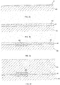
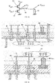
- FIG. 1 An example of an integrated VDMOS according to the invention is illustrated in Figure 1 .
- the drawing shows two sets I and II of 3 semiconductor fins 1, which are uniform with a semiconductor substrate 2, which is taken to be a p-doped silicon substrate in this detailed description, even though the invention is not limited thereto.
- N type well regions 3a and 3b are created at the location of the fins.
- Other areas of the substrate may comprise p-wells or adjacent p and n-wells, depending on the required functionality of the active devices produced on the active portion of the fins. This active portion is situated at the top of the fins, whereas the base of the fins is embedded in a layer 4 of dielectric material, commonly referred to as the shallow trench isolation (STI) dielectric layer.
- STI shallow trench isolation
- Contact areas 5 are depicted in a simplified way on the top area of the fins. These are epitaxially grown areas for contacting selected sections of the fins, primarily source or drain areas of transistors which carry current in the direction of the fins, controlled through gate electrodes and gate dielectric layers extending transversally with respect to the fins. Gate electrodes are not shown in the particular section illustrated in Figure 1 , but their function and physical characteristics are well known to the skilled reader.
- the group of fins II on the right hand side is a standard group of fins, produced and powered in the manner described in EP3324436A1 . Adjacent the group of fins II is a buried power rail 6, that is embedded partially in the n-well 3b and in the STI layer 4.
- the buried rail 6 is connected to the back side of the substrate 2 by a TSV connection 7 that is isolated from the p-substrate 2 by a dielectric liner 8.
- a passivation layer 9 that carries the Power Delivery Network, of which a first layer is shown in the drawing.
- the PDN comprises one or more such layers formed of conductors 10 and via-connections 11 embedded in a layer of dielectric material 12, and ultimately connected to a power or a reference (normally ground) terminal. This is described in more detail in EP3324436A1 .
- the buried rail 6 is coupled to a first metallization layer, sometimes referred to as the M0 level, and comprising so-called 'local interconnects', which are conductors 13 embedded in a dielectric layer 14, referred to in this context as an ILD layer (interlayer dielectric).
- a first metallization layer sometimes referred to as the M0 level
- ILD layer interlayer dielectric
- the local interconnects 13 are coupled to additional metallization layers M1, M2 etc (not shown), which form the back end of line portion of the chip.
- the elements referred to so far are well-known to the skilled person and additional detail is therefore not required for their description.
- the group of fins I on the left-hand side is also formed on an n-well 3a on the upper surface of the substrate, and a buried rail 20 is again located adjacent the fins 1.
- an n-type VDMOS transistor is produced in an area situated around a selected portion of the rail 20.
- the production process will be described in more detail hereafter.
- the obtained structure is visible in Figure 1 .
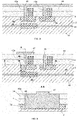
- a plug 21 formed of a dielectric material for example silicon nitride.
- the rest of the trench is filled with conductive material, the same preferably as the standard rail 6, and coming up to the same level as the standard rail 6.
- the 'modified' rail 20 is connected to the M0 level in the same way as the standard rail, by a TSV connection 22.
- the SiN plug itself is in direct physical contact with a TSV connection 23 that is identical to the TSV connection 7 that connects the standard rail 6 to the back side PDN.
- a liner 24 separates the TSV 23 from the substrate 2.
- On the back side of the substrate 2, another distinctive feature is visible.
- An n-well 25 is formed on this back side, with the TSV 23 penetrating the n-well 25.
- the upper side of the n-well 25 is spaced apart from the lower side of the n-well 3a at the front of the substrate 2.
- the n-well 25 furthermore extends laterally away from the TSV 23, and there it envelops a contact area 26 located adjacent the TSV 23 and open to the back surface of the substrate 2, which may be a metal silicide area.
- the contact area 26 is connected to the PDN by a short via connection 27 through a passivation layer 9 on the back surface of the substrate 2.
- the TSV 23 and the short via connection 27 are connected to separate conductors 10 in the PDN.
- the resulting structure is equivalent to a VDMOS transistor, with the p-type substrate 2 acting as a first diffusion and the n-well 25 as the second diffusion of the 'double diffusion' structure.
- the silicide contact area 26 on the backside is the source electrode of the VDMOS.
- the TSV 23 is the gate electrode and the liner 24 plays the part of the gate dielectric.
- the presence of the SiN plug 21 creates a drift region in the upper n-well 3a, between the channel and the portion of the rail 20 above the plug, the latter playing the part of the drain of the VDMOS. A vertical current path is thereby created from the source 26 to the drain 20.
- the fins of the first group I shown in Figure 1 do not perform a function in the operation of the VDMOS. They are included in the drawing in order to illustrate that the VDMOS can be integrated in an existing fabrication process of an IC with minimal changes to the layout and process steps.
- the creation of the n-well 3a and of the trench for forming the rail 20 is already included. It is only needed to perform a number of additional steps in order to create the VDMOS, as will be described in more detail hereafter.
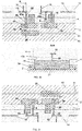
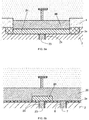
- a p-type VDMOS according to the invention may be produced, although this requires additional well implant steps.
- the well 25 on the backside of the substrate is now a p-well, while a deep n-well 30 is required on the front side, with the p-well 3a embedded therein so that the SiN plug 21 is now enveloped by the p-well 3a.
- the deep n-well 31 is needed to isolate the p-well 3a from the substrate.
- the channel is formed in the area of the substrate 2 and of the deep n-well 30 surrounding the TSV 23.
- One part of the channel is now “enhancement type" (substrate 2) and the other part is “depletion type” (deep N-well 30).
- the conductivity of the channel is still controlled by the gate 23. Carriers go from one p+ junction to another p+ junction and punchthrough current lines (not controlled by the gate) are cut off by the deep n-well 30..
- source and drain are not exclusively dedicated to the silicide area 26 and the rail 20, but these functions may be reversed, i.e. the rail may be the source of the transistor, and the silicide area may be the drain. Physically, this requires a drift region in the well 25 at the back side of the substrate 2, so it is preferred to place the silicide area 26 further away from the TSV 23, as illustrated in Figure 2c for an n-type VDMOS according to the invention.
- the drift region 28 is indicated.
- Figures 3a to 3o illustrate a number of key steps of a fabrication process that integrates a VDMOS in an integrated circuit chip in the manner shown in Figure 1 .
- the materials cited hereafter are not intended to limit the scope of the invention.
- a silicon process wafer 40 is provided and a thin SiGe layer 41 is produced on its surface preferably by epitaxial growth. Again by epitaxial growth, a monocrystalline silicon layer 42 is produced on the SiGe layer 41, see Figure 3b .
- the SiGe layer 41 may have a thickness of a few tens of nanometres.
- the epitaxial Si-layer 42 may have a thickness of about 100nm.
- the Si-layer 42 may be subjected to a doping step (not shown) by implanting the complete layer with p-type doping elements, to turn the layer into a lightly p-doped layer. More preferably, the p-type doping is applied in situ during the epitaxial growth. Then an n-type dopant implant step is performed in a limited area (see Figure 3c ) by masking the wafer except in this limited area, thereby creating an n-well 25 which will become the back side n-well 25 shown in Figure 1 .
- the dopant densities are in accordance with standard values for the creation of well regions, well-known to the skilled person.
- a first dopant activation anneal step may be performed at this point, to activate the dopant elements.
- Si-layer 43 is obtained on the SiGe layer 41, of a thickness that may be in the order of 500nm.
- P-type doping of the Si-layer 43 is realized by in-situ doping during the epitaxy, or the Si-layer 43 may be subjected to a p-type dopant implantation (not shown), in order to turn the full Si layer into a lightly p-doped layer, which may again be followed by a dopant activation anneal.
- this layer 43 is patterned to form multiple fins 1 of which two groups are shown in Figure 3e : group I and group II.
- the fins are uniform with the substrate, now reduced to a lower thickness and referenced by numeral 2, in correspondence with Figure 1 .
- Additional dopant implant steps are performed to create n-well regions 3a and 3b which include the respective fin groups I and II.
- Other fins or fin groups not shown in the drawings may be implanted with p-type dopant elements, for example in accordance with a layout scheme of logic cells. At this point, annealing may be performed to activate the dopant elements in the various well regions.
- dopant activation anneal steps may take place at other points in the process, for example after or during the STI deposition process, as is well known in the art.
- the invention is not limited therefore to a particular approach of these method steps which are known per se in the art.
- Figure 3f this is then followed by standard process steps for producing the STI layer 4, and for processing the active portion of the fins to form transistors, which may include the fabrication of a dummy gate, the processing of contact areas 5 for source and drain areas by epitaxy in areas adjacent the dummy gate, and the completion of the transistor by the replacement of the dummy gate by a gate stack comprising a gate dielectric and electrically conductive gate electrode.
- Figure 3f illustrates source or drain areas 5 on both groups of fins I and II.
- an ILD layer 44 is deposited.
- elongate trenches 45a and 45b are then produced by etching through the ILD layer 44 and the STI 4. The etching stops within the n-wells 3a and 3b.
- Thee trenches 45a and 45b are formed by lithography and etch processes and at dimensions known from the prior art methods for creating buried power rails by filling the trenches with an electrically conductive material. This is in fact the aim of these trenches on most of the wafer surface.
- the trenches extend along a distance perpendicular to the plane of the drawings, in accordance with a given layout of the buried rails.
- the trench 45a is fully enveloped by the n-well 3a, i.e. the n-well 3a separates the trench 45a from the substrate 2.
- a number of additional process steps performed after formation of the trenches then enables the creation of the VDMOS at a selected location of the wafer, in accordance with the invention, and as illustrated first in Figure 3h .
- a layer 46 of silicon nitride is deposited on the wafer, filling the trenches and forming a blanket layer on the wafer surface.
- the blanket layer is then patterned ( Fig. 3i ), so that the SiN is thinned and preferably removed everywhere from the upper surface of the wafer except in an area 47 above the trench adjacent the first group of fins, where a patch of SiN remains.
- Figure 3i shows a section view of the trench 45a, filled with the SiN 46, and with the patch 47 of SiN on top. It is seen in this drawing that the trench is effectively enveloped on all sides by the n-well 3a.
- the SiN is then progressively etched back from the upper surface downward ( Fig. 3j ), until it is removed from the trenches 45a and 45b, except in the area where the patch 47 of SiN had been maintained. Because of the presence of the patch 47, a plug 21 of SiN remains at the bottom of the trench 45a at the end of the etch-back process. The thickness of the patch 47 determines the thickness of the SiN plug 21.
- the standard steps are performed of filling the trenches with an electrically conductive material, preferably a metal, possibly preceded where necessary by the formation of an dielectric liner on the sidewalls of the trenches.
- the metal is etched back to form the buried rails 6 in the trench 45b and 20 in the trench 45a, as seen in Figure 3k .
- the same drawing illustrates that additional ILD material is deposited on top of the rails, and the rails are connected by via connections 15 and 22 to conductors 13 in the M0 level.
- the back end of line processing is done, after which the wafer is flipped and bonded to another wafer, with the BEOL side attached thereto, so that the process wafer 40 is now directed upward, as illustrated in Figure 3l .
- the process wafer is thinned by grinding and/or CMP, and eventually by an etch process that is stopped by the SiGe layer 41.
- this contact area is formed of a metal silicide. This may be done in a manner known as such in the art, wherein a silicide forming metal is first deposited on the entire wafer surface, then patterned to leave the metal only in the contact area, followed by silicidation through heating, and if necessary the removal of unreacted silicide forming metal.
- Suitable silicide forming metals are Ni, NiPt, Co or Ti.
- an additional via 51 is produced through the passivation layer 9, above the silicide contact area 26, and this contact area acts as an etch stop layer for the etch process applied for producing the via opening 51, so that the etch process results in deep via openings 50a and 50b reaching down to the surface of the buried rails, and a less deep via 51 reaching down to the silicide area 26.
- the via opening 50a produced at the location of the SiN plug 21 exposes the SiN plug at the end of the etch process.
- a dielectric liner is deposited on the sidewalls and the bottom of the via openings 50a and 50b.
- the liner is indicated by numeral 8 for the via opening 50b and by numeral 24 for the via opening 50a, but these liners are the same material and deposited simultaneously.
- the liner 8/24 is removed from the bottom of the TSV openings by a suitable etch process known in the art, preferably a plasma etch process that creates a protective polymer layer on the sidewalls while removing the liner from the bottom.
- a suitable etch process known in the art, preferably a plasma etch process that creates a protective polymer layer on the sidewalls while removing the liner from the bottom.
- a suitable process of this type is described for example in patent document EP3035369 .
- the material of the dielectric plug 21 must be resistant to this plasma etch so that the plug is not removed by the etch process.
- SiN is a suitable material for the dielectric plug, as SiN is resistant to at least one plasma etch process suitable for removing the liner from the bottom of the via openings 50a and 50b.
- the via openings 50a, 50b and 51 are then filled with an electrically conductive material, preferably a metal, and the process is completed with the further processing of the PDN, leading to the configuration shown in Figure 1 , including the conductors 10 and vias 11 embedded in a dielectric layer 12. This completes the fabrication process of the VDMOS.
- FIG. 4a illustrates a basic circuit of such a converter, comprising a pull-up transistor 60 and a pull-down transistor 61 coupled in series between a power voltage V PW and ground.
- the gates of the transistors are coupled to control voltages V gp and V gn .
- the pull-up transistor is a p-type transistor while the pull-down transistor is an n-type transistor.
- An inductance 62 (a coil) is coupled between the common node of the transistors and a load 63.
- the load consists of the logic cells and other active devices on the chip.
- a capacitor may be coupled between the output of the inductance 62 and ground but this is not the case in the circuit shown in Figure 4a .
- the control voltages V gp and V gn are synchronized in a manner to convert the power voltage V PW to a lower voltage V MOS .
- the voltage at the common node is referred to as V X .
- Figure 4b shows the implementation of the buck converter circuit of Figure 4a , using VDMOS transistors in accordance with the invention.
- the voltage levels shown in Figure 4a are indicated also in Figure 4b , making it clear that the configuration effectively corresponds to the buck converter circuit.
- n-type VDMOS transistor (as in Figure 2a ) and a p-type VDMOS transistor (as in Figure 2b ) according to the invention are integrated together on the same chip and coupled to a coil in the manner shown in Figure 4a .
- the coil is integrated in the back end of line portion of the chip, in the form of an interconnected assembly of suitably formed conductors.
- the converter supplies power at voltage V MOS to the active devices on the chip.
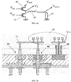
- Figure 5a shows the converter circuit wherein both switches are 60 and 61 n-type transistors.
- a first implementation with VDMOS transistors according to the invention is shown in Figure 5b . It includes three standard TSVs for realizing the node at voltage V X and the connection to the power voltage V PW .
- the coil 62 is now located on the back side of the chip, and may be incorporated in the back side power delivery network, as shown in the drawing. Alternatively in this case, the coil 62 could be located outside the chip.
- Figure 5c illustrates an implementation of the circuit of Figure 5a , using two n-type VDMOS transistors according to the invention, and wherein the coil 62 is incorporated in the back end of line.
- the rail acts as the source electrode and the silicide area acts as the drain electrode, i.e. as in the embodiment of Figure 2c .
- the transistor 60 is now configured so that the rail acts as the source and the silicide area acts as the drain.
- the drift region 28 is indicated.
- the invention is not limited to chips which have a complete PDN on the back side of the substrate. It is sufficient that at least two conductors 10 are available on the back side, which are accessible from the exterior of the chip, in order to apply a gate voltage to the TSV connection 23 and a source voltage to the contact area 26, or obtain a drain voltage at the contact area 26 depending on the function of the latter.
- the dielectric plug 21 is shorter than the rail 20 and the dielectric plug fills a cavity on the underside of the rail, as a consequence of the production process described above.
- a rail formed of an electrically conductive material, and buried at least partially in the first well region, and provided with a dielectric plug in physical contact with the underside of the rail, and configured so that the rail does not extend beyond the lower side of the first well region 3a'.
- Other embodiments may fulfill the scope of this feature, examples of which are shown in Figures 6a and 6b .
- the plug extends along the full length of the rail 20.
- the plug 21 itself may in this case extend approximately down to the lower side of the n-well 3a as shown in the drawing. In reality, this means that the bottom of the plug is in or near the gradient area defined by the diffusion tail of the implanted ions used to create the well.
- Figure 6a also shows part of the VDMOS gate electrode 23 and the gate dielectric 24.
- the rail 20 is a continuous rail, which may be electrically connected to a standard TSV 7 (shown with its liner 8 in Fig. 6b ).
- the dielectric plug 21 extends along a portion of the rail's underside, and the VDMOS gate electrode 23 is in contact with the plug 21, as in the embodiment of Figure 1 .
- the rail 20 in its entirety is once again separated from the substrate 2 by the n-well 3a. This is a special case, applicable only when the rail 20 is the source of the VDMOS and when the source is held to ground potential. In this case, rail 20 can be a grounded rail of the Power delivery network for example.
- the description of a layer being present, deposited or produced 'on' another layer or substrate includes the options of
Landscapes
- Engineering & Computer Science (AREA)
- Power Engineering (AREA)
- Metal-Oxide And Bipolar Metal-Oxide Semiconductor Integrated Circuits (AREA)
- Insulated Gate Type Field-Effect Transistor (AREA)
- Internal Circuitry In Semiconductor Integrated Circuit Devices (AREA)
Priority Applications (2)
| Application Number | Priority Date | Filing Date | Title |
|---|---|---|---|
| EP18214426.1A EP3671859B1 (de) | 2018-12-20 | 2018-12-20 | Verfahren zur herstellung eines vertikal isolierten gate-feldeffekttransistors, der in einen halbleiterchip integriert ist |
| US16/716,262 US11121086B2 (en) | 2018-12-20 | 2019-12-16 | Vertical isolated gate field effect transistor integrated in a semiconductor chip |
Applications Claiming Priority (1)
| Application Number | Priority Date | Filing Date | Title |
|---|---|---|---|
| EP18214426.1A EP3671859B1 (de) | 2018-12-20 | 2018-12-20 | Verfahren zur herstellung eines vertikal isolierten gate-feldeffekttransistors, der in einen halbleiterchip integriert ist |
Publications (2)
| Publication Number | Publication Date |
|---|---|
| EP3671859A1 true EP3671859A1 (de) | 2020-06-24 |
| EP3671859B1 EP3671859B1 (de) | 2025-04-30 |
Family
ID=64755155
Family Applications (1)
| Application Number | Title | Priority Date | Filing Date |
|---|---|---|---|
| EP18214426.1A Active EP3671859B1 (de) | 2018-12-20 | 2018-12-20 | Verfahren zur herstellung eines vertikal isolierten gate-feldeffekttransistors, der in einen halbleiterchip integriert ist |
Country Status (2)
| Country | Link |
|---|---|
| US (1) | US11121086B2 (de) |
| EP (1) | EP3671859B1 (de) |
Cited By (12)
| Publication number | Priority date | Publication date | Assignee | Title |
|---|---|---|---|---|
| DE102019127886A1 (de) * | 2019-09-30 | 2021-04-01 | Taiwan Semiconductor Manufacturing Co., Ltd. | Halbleitervorrichtung enthaltend einen rückseitigen stromversorgungskreis |
| CN114093948A (zh) * | 2020-10-30 | 2022-02-25 | 成都芯源系统有限公司 | 场板沟槽场效应晶体管及其制造方法 |
| EP4002435A1 (de) * | 2020-11-13 | 2022-05-25 | Samsung Electronics Co., Ltd. | Halbleiterbauelement mit rückseitigem stromverteilungsnetz und verfahren zur herstellung davon |
| EP4044218A1 (de) * | 2021-02-11 | 2022-08-17 | Imec VZW | Verfahren zur herstellung einer halbleiterdurchkontaktierung |
| CN115149514A (zh) * | 2022-08-31 | 2022-10-04 | 之江实验室 | 一种针对晶圆处理器的共享控制式供电装置 |
| EP4156257A3 (de) * | 2021-09-24 | 2023-04-05 | INTEL Corporation | Halbleiterchips und vorrichtungen mit einer spule zur induktiven kopplung |
| WO2023066797A1 (en) * | 2021-10-22 | 2023-04-27 | International Business Machines Corporation | Early backside first power delivery network |
| EP4187581A1 (de) * | 2021-11-26 | 2023-05-31 | Imec VZW | Verbindungsstruktur eines halbleiterbauelements und verfahren zur herstellung dieser struktur |
| WO2024068454A1 (en) * | 2022-09-30 | 2024-04-04 | International Business Machines Corporation | Power gating dummy power transistors for back side power delivery networks |
| WO2025185889A1 (en) * | 2024-03-08 | 2025-09-12 | International Business Machines Corporation | Enhanced power rail connection |
| TWI907795B (zh) * | 2022-12-30 | 2025-12-11 | 美商萬國商業機器公司 | 晶圓正面和背面之間基於單元的信號連接 |
| US12598981B2 (en) * | 2022-09-15 | 2026-04-07 | Qualcomm Incorporated | Port landing-free low-skew signal distribution with backside metallization and buried rail |
Families Citing this family (36)
| Publication number | Priority date | Publication date | Assignee | Title |
|---|---|---|---|---|
| US11862561B2 (en) * | 2020-05-28 | 2024-01-02 | Taiwan Semiconductor Manufacturing Co., Ltd. | Semiconductor devices with backside routing and method of forming same |
| US11715755B2 (en) * | 2020-06-15 | 2023-08-01 | Taiwan Semiconductor Manufacturing Co., Ltd. | Structure and method for forming integrated high density MIM capacitor |
| US11728244B2 (en) * | 2020-07-17 | 2023-08-15 | Taiwan Semiconductor Manufacturing Co., Ltd. | Semiconductor device and method for forming the same |
| KR102821727B1 (ko) | 2020-08-03 | 2025-06-19 | 삼성전자주식회사 | 반도체 소자 및 반도체 패키지 |
| US11443777B2 (en) * | 2020-09-11 | 2022-09-13 | Arm Limited | Backside power rail architecture |
| US11817392B2 (en) | 2020-09-28 | 2023-11-14 | Taiwan Semiconductor Manufacturing Co., Ltd. | Integrated circuit |
| KR102894035B1 (ko) * | 2020-10-15 | 2025-12-03 | 삼성전자주식회사 | 반도체 소자 |
| US11410986B2 (en) * | 2020-10-21 | 2022-08-09 | Taiwan Semiconductor Manufacturing Company, Ltd. | Power cell for semiconductor devices |
| KR20220057116A (ko) | 2020-10-29 | 2022-05-09 | 삼성전자주식회사 | 반도체 패키지 |
| KR102934454B1 (ko) | 2020-11-03 | 2026-03-06 | 삼성전자주식회사 | Bs-pdn 구조를 가진 집적회로 칩 |
| US11961802B2 (en) | 2020-12-04 | 2024-04-16 | Tokyo Electron Limited | Power-tap pass-through to connect a buried power rail to front-side power distribution network |
| KR102939312B1 (ko) | 2020-12-28 | 2026-03-12 | 삼성전자주식회사 | 집적회로 장치 |
| KR102864985B1 (ko) * | 2020-12-31 | 2025-09-25 | 삼성전자주식회사 | 반도체 장치 |
| US12374623B2 (en) | 2021-01-18 | 2025-07-29 | Samsung Electronics Co., Ltd. | Stacked semiconductor device architecture |
| US12464771B2 (en) * | 2021-01-22 | 2025-11-04 | Taiwan Semiconductor Manufacturing Company, Ltd. | Semiconductor devices and methods of manufacturing thereof |
| US11881455B2 (en) | 2021-05-20 | 2024-01-23 | Samsung Electronics Co., Ltd. | Through silicon buried power rail implemented backside power distribution network semiconductor architecture and method of manufacturing the same |
| US11915966B2 (en) | 2021-06-09 | 2024-02-27 | International Business Machines Corporation | Backside power rail integration |
| KR102916492B1 (ko) | 2021-06-11 | 2026-01-26 | 삼성전자주식회사 | 관통 전극들을 포함하는 반도체 소자 |
| US11984384B2 (en) * | 2021-09-09 | 2024-05-14 | Synopsys, Inc. | Power routing for 2.5D or 3D integrated circuits including a buried power rail and interposer with power delivery network |
| US11764298B2 (en) | 2021-09-17 | 2023-09-19 | International Business Machines Corporation | VTFET with buried power rails |
| US11990412B2 (en) | 2021-09-29 | 2024-05-21 | International Business Machines Corporation | Buried power rails located in a base layer including first, second, and third etch stop layers |
| KR102902644B1 (ko) | 2021-10-05 | 2025-12-23 | 삼성전자주식회사 | 반도체 소자 |
| US12057371B2 (en) | 2021-10-26 | 2024-08-06 | International Business Machines Corporation | Semiconductor device with early buried power rail (BPR) and backside power distribution network (BSPDN) |
| US12268016B2 (en) | 2021-12-29 | 2025-04-01 | International Business Machines Corporation | Buried power rail formation for vertical field effect transistors |
| US12463136B2 (en) | 2022-04-29 | 2025-11-04 | Samsung Electronics Co., Ltd. | Integrated circuit devices including backside power rail and methods of forming the same |
| US12412836B2 (en) | 2022-05-11 | 2025-09-09 | International Business Machines Corporation | Backside power plane |
| US20230377967A1 (en) * | 2022-05-23 | 2023-11-23 | Micron Technology, Inc. | Method of forming through silicon via and trench using the same mask layer |
| KR20240018249A (ko) | 2022-08-02 | 2024-02-13 | 삼성전자주식회사 | 집적회로 소자 |
| US12362278B2 (en) | 2022-08-31 | 2025-07-15 | International Business Machines Corporation | Transistors with dual power and signal lines |
| US12453146B2 (en) | 2022-09-22 | 2025-10-21 | International Business Machines Corporation | Epi growth uniformity with source/drain placeholder |
| US20240105727A1 (en) * | 2022-09-23 | 2024-03-28 | Apple Inc. | Vertical Transistor Cell Structures Utilizing Topside and Backside Resources |
| US12400960B2 (en) | 2022-09-28 | 2025-08-26 | International Business Machines Corporation | Vertical-transport field-effect transistor with backside gate contact |
| US12484248B2 (en) | 2022-10-25 | 2025-11-25 | International Business Machines Corporation | Source/drain contact at tight cell boundary |
| US12419024B2 (en) | 2022-11-08 | 2025-09-16 | International Business Machines Corporation | High density static random-access memory |
| US12550351B2 (en) | 2023-07-31 | 2026-02-10 | International Business Machines Corporation | Diffusion break between passive device and logic device with backside contact |
| TWI852720B (zh) * | 2023-08-09 | 2024-08-11 | 立錡科技股份有限公司 | 接面場效電晶體裝置及其製造方法 |
Citations (6)
| Publication number | Priority date | Publication date | Assignee | Title |
|---|---|---|---|---|
| US4767722A (en) | 1986-03-24 | 1988-08-30 | Siliconix Incorporated | Method for making planar vertical channel DMOS structures |
| US6373097B1 (en) * | 1996-09-19 | 2002-04-16 | Infineon Technologies Ag | Field-effect-controllable, vertical semiconductor component, and monolithically integrated half bridge |
| US20120146711A1 (en) * | 2010-12-13 | 2012-06-14 | International Business Machines Corporation | Power Domain Controller With Gated Through Silicon Via Having FET With Horizontal Channel |
| WO2012144951A1 (en) * | 2011-04-21 | 2012-10-26 | Silex Microsystems Ab | A starting substrate for semiconductor engineering having substrate-through connections and a method for making same |
| EP3035369A1 (de) | 2014-12-18 | 2016-06-22 | IMEC vzw | Plasmabehandlungsverfahren |
| EP3324436A1 (de) | 2016-11-21 | 2018-05-23 | IMEC vzw | Chip mit integrierter schaltung mit stromversorgungsnetzwerk auf der rückseite des chips |
Family Cites Families (14)
| Publication number | Priority date | Publication date | Assignee | Title |
|---|---|---|---|---|
| US6380569B1 (en) * | 1999-08-10 | 2002-04-30 | Rockwell Science Center, Llc | High power unipolar FET switch |
| DE102008047591B4 (de) * | 2007-09-18 | 2019-08-14 | Samsung Electronics Co., Ltd. | Verfahren zum Herstellen einer Halbleitervorrichtung mit reduzierter Dicke |
| US8796764B2 (en) | 2008-09-30 | 2014-08-05 | Infineon Technologies Austria Ag | Semiconductor device comprising trench gate and buried source electrodes |
| EP2378557B1 (de) * | 2010-04-19 | 2015-12-23 | Imec | Verfahren zur Herstellung eines vertikalen TFET |
| US8471331B2 (en) * | 2011-08-15 | 2013-06-25 | Semiconductor Components Industries, Llc | Method of making an insulated gate semiconductor device with source-substrate connection and structure |
| US9130060B2 (en) | 2012-07-11 | 2015-09-08 | Taiwan Semiconductor Manufacturing Company, Ltd. | Integrated circuit having a vertical power MOS transistor |
| KR101847630B1 (ko) * | 2013-04-01 | 2018-05-24 | 삼성전자주식회사 | 반도체 소자 및 반도체 모듈 |
| KR20150035198A (ko) | 2013-09-27 | 2015-04-06 | 삼성전자주식회사 | 반도체 소자 및 그 제조방법 |
| US9379246B2 (en) * | 2014-03-05 | 2016-06-28 | Sandisk Technologies Inc. | Vertical thin film transistor selection devices and methods of fabrication |
| CN107660312B (zh) * | 2015-06-19 | 2022-08-12 | 英特尔公司 | 使用穿硅过孔栅极的竖直晶体管 |
| US9953900B2 (en) * | 2016-03-29 | 2018-04-24 | Globalfoundries Inc. | Transistor structures gated using a conductor-filled via or trench |
| US10461186B1 (en) * | 2018-05-31 | 2019-10-29 | Globalfoundries Inc. | Methods of forming vertical field effect transistors with self-aligned contacts and the resulting structures |
| US10658246B2 (en) * | 2018-08-27 | 2020-05-19 | International Business Machines Corporation | Self-aligned vertical fin field effect transistor with replacement gate structure |
| US10916638B2 (en) * | 2018-09-18 | 2021-02-09 | International Business Machines Corporation | Vertical fin field effect transistor devices with reduced top source/drain variability and lower resistance |
-
2018
- 2018-12-20 EP EP18214426.1A patent/EP3671859B1/de active Active
-
2019
- 2019-12-16 US US16/716,262 patent/US11121086B2/en active Active
Patent Citations (6)
| Publication number | Priority date | Publication date | Assignee | Title |
|---|---|---|---|---|
| US4767722A (en) | 1986-03-24 | 1988-08-30 | Siliconix Incorporated | Method for making planar vertical channel DMOS structures |
| US6373097B1 (en) * | 1996-09-19 | 2002-04-16 | Infineon Technologies Ag | Field-effect-controllable, vertical semiconductor component, and monolithically integrated half bridge |
| US20120146711A1 (en) * | 2010-12-13 | 2012-06-14 | International Business Machines Corporation | Power Domain Controller With Gated Through Silicon Via Having FET With Horizontal Channel |
| WO2012144951A1 (en) * | 2011-04-21 | 2012-10-26 | Silex Microsystems Ab | A starting substrate for semiconductor engineering having substrate-through connections and a method for making same |
| EP3035369A1 (de) | 2014-12-18 | 2016-06-22 | IMEC vzw | Plasmabehandlungsverfahren |
| EP3324436A1 (de) | 2016-11-21 | 2018-05-23 | IMEC vzw | Chip mit integrierter schaltung mit stromversorgungsnetzwerk auf der rückseite des chips |
Cited By (23)
| Publication number | Priority date | Publication date | Assignee | Title |
|---|---|---|---|---|
| US11742285B2 (en) | 2019-09-30 | 2023-08-29 | Taiwan Semiconductor Manufacturing Company, Ltd. | Semiconductor device including back side power supply circuit |
| US11004789B2 (en) | 2019-09-30 | 2021-05-11 | Taiwan Semiconductor Manufacturing Co., Ltd. | Semiconductor device including back side power supply circuit |
| DE102019127886B4 (de) | 2019-09-30 | 2021-11-18 | Taiwan Semiconductor Manufacturing Co., Ltd. | Halbleitervorrichtung enthaltend einen rückseitigen Stromversorgungskreis |
| DE102019127886A1 (de) * | 2019-09-30 | 2021-04-01 | Taiwan Semiconductor Manufacturing Co., Ltd. | Halbleitervorrichtung enthaltend einen rückseitigen stromversorgungskreis |
| US12500168B2 (en) | 2019-09-30 | 2025-12-16 | Taiwan Semiconductor Manufacturing Company, Ltd. | Semiconductor device including back side power supply circuit |
| CN114093948A (zh) * | 2020-10-30 | 2022-02-25 | 成都芯源系统有限公司 | 场板沟槽场效应晶体管及其制造方法 |
| EP4002435A1 (de) * | 2020-11-13 | 2022-05-25 | Samsung Electronics Co., Ltd. | Halbleiterbauelement mit rückseitigem stromverteilungsnetz und verfahren zur herstellung davon |
| US12142564B2 (en) | 2020-11-13 | 2024-11-12 | Samsung Electronics Co., Ltd. | Backside power distribution network semiconductor package and method of manufacturing the same |
| US11769728B2 (en) | 2020-11-13 | 2023-09-26 | Samsung Electronics Co., Ltd. | Backside power distribution network semiconductor package and method of manufacturing the same |
| EP4044218A1 (de) * | 2021-02-11 | 2022-08-17 | Imec VZW | Verfahren zur herstellung einer halbleiterdurchkontaktierung |
| US12598966B2 (en) | 2021-02-11 | 2026-04-07 | Imec Vzw | Method for producing a through semiconductor via connection |
| EP4156257A3 (de) * | 2021-09-24 | 2023-04-05 | INTEL Corporation | Halbleiterchips und vorrichtungen mit einer spule zur induktiven kopplung |
| US12347796B2 (en) | 2021-09-24 | 2025-07-01 | Intel Corporation | Semiconductor dies and devices with a coil for inductive coupling |
| WO2023066797A1 (en) * | 2021-10-22 | 2023-04-27 | International Business Machines Corporation | Early backside first power delivery network |
| US12482746B2 (en) | 2021-10-22 | 2025-11-25 | International Business Machines Corporation | Early backside first power delivery network |
| US12494424B2 (en) | 2021-11-26 | 2025-12-09 | Imec Vzw | Interconnect structure of a semiconductor component and methods for producing the structure |
| EP4187581A1 (de) * | 2021-11-26 | 2023-05-31 | Imec VZW | Verbindungsstruktur eines halbleiterbauelements und verfahren zur herstellung dieser struktur |
| CN115149514A (zh) * | 2022-08-31 | 2022-10-04 | 之江实验室 | 一种针对晶圆处理器的共享控制式供电装置 |
| US12598981B2 (en) * | 2022-09-15 | 2026-04-07 | Qualcomm Incorporated | Port landing-free low-skew signal distribution with backside metallization and buried rail |
| WO2024068454A1 (en) * | 2022-09-30 | 2024-04-04 | International Business Machines Corporation | Power gating dummy power transistors for back side power delivery networks |
| US12382719B2 (en) | 2022-09-30 | 2025-08-05 | International Business Machines Corporation | Power gating dummy power transistors for back side power delivery networks |
| TWI907795B (zh) * | 2022-12-30 | 2025-12-11 | 美商萬國商業機器公司 | 晶圓正面和背面之間基於單元的信號連接 |
| WO2025185889A1 (en) * | 2024-03-08 | 2025-09-12 | International Business Machines Corporation | Enhanced power rail connection |
Also Published As
| Publication number | Publication date |
|---|---|
| EP3671859B1 (de) | 2025-04-30 |
| US20200203276A1 (en) | 2020-06-25 |
| US11121086B2 (en) | 2021-09-14 |
Similar Documents
| Publication | Publication Date | Title |
|---|---|---|
| US11121086B2 (en) | Vertical isolated gate field effect transistor integrated in a semiconductor chip | |
| US11257764B2 (en) | Integrated circuit with backside power delivery network and backside transistor | |
| EP2913847B1 (de) | Verfahren zur Herstellung eines Halbleiterbauelements und Halbleiterbauelement | |
| US9396997B2 (en) | Method for producing a semiconductor component with insulated semiconductor mesas | |
| US10079230B2 (en) | Double-sided vertical semiconductor device with thinned substrate | |
| US6747314B2 (en) | Method to form a self-aligned CMOS inverter using vertical device integration | |
| TWI609489B (zh) | 具有薄基體之垂直半導體元件 | |
| US9941383B2 (en) | Fast switching IGBT with embedded emitter shorting contacts and method for making same | |
| US6204137B1 (en) | Method to form transistors and local interconnects using a silicon nitride dummy gate technique | |
| CN111108593A (zh) | 窄深沟槽的沉降物至掩埋层连接区域 | |
| US6693011B2 (en) | Power MOS element and method for producing the same | |
| WO2008055095A2 (en) | Junction isolated poly-silicon gate jfet | |
| CN103782386A (zh) | 具有集成栅极电阻器和二极管接法mosfet的功率mosfet | |
| US6300657B1 (en) | Self-aligned dynamic threshold CMOS device | |
| KR20110001921A (ko) | 서로 연결되는 트랜지스터를 포함한 집적 회로를 포함하는 전자 장치 | |
| CN102237357A (zh) | 一种集成电路装置及其制造方法 | |
| US20040146701A1 (en) | Semiconductor substrate having SOI structure and manufacturing method and semiconductor device thereof | |
| KR20170121224A (ko) | 수직형 파워 디바이스 내의 표면 디바이스들 | |
| EP3591696B1 (de) | Verfahren zur herstellung einer halbleiter-durchkontaktierung | |
| KR20110001893A (ko) | 우물 영역을 포함하는 전자 장치 | |
| TWI435373B (zh) | 具有埋藏摻雜層之完全耗盡型絕緣體上矽裝置 | |
| US20040188768A1 (en) | Diode structure for SOI circuits | |
| EP0607583A2 (de) | Verbesserte Isolation für Hoch- und Niedrigspannungkombinierte Verfahren | |
| CN117637858A (zh) | 竖直半导体器件及其制造方法 |
Legal Events
| Date | Code | Title | Description |
|---|---|---|---|
| PUAI | Public reference made under article 153(3) epc to a published international application that has entered the european phase |
Free format text: ORIGINAL CODE: 0009012 |
|
| STAA | Information on the status of an ep patent application or granted ep patent |
Free format text: STATUS: THE APPLICATION HAS BEEN PUBLISHED |
|
| AK | Designated contracting states |
Kind code of ref document: A1 Designated state(s): AL AT BE BG CH CY CZ DE DK EE ES FI FR GB GR HR HU IE IS IT LI LT LU LV MC MK MT NL NO PL PT RO RS SE SI SK SM TR |
|
| AX | Request for extension of the european patent |
Extension state: BA ME |
|
| STAA | Information on the status of an ep patent application or granted ep patent |
Free format text: STATUS: REQUEST FOR EXAMINATION WAS MADE |
|
| 17P | Request for examination filed |
Effective date: 20201224 |
|
| RBV | Designated contracting states (corrected) |
Designated state(s): AL AT BE BG CH CY CZ DE DK EE ES FI FR GB GR HR HU IE IS IT LI LT LU LV MC MK MT NL NO PL PT RO RS SE SI SK SM TR |
|
| STAA | Information on the status of an ep patent application or granted ep patent |
Free format text: STATUS: EXAMINATION IS IN PROGRESS |
|
| 17Q | First examination report despatched |
Effective date: 20211125 |
|
| GRAP | Despatch of communication of intention to grant a patent |
Free format text: ORIGINAL CODE: EPIDOSNIGR1 |
|
| STAA | Information on the status of an ep patent application or granted ep patent |
Free format text: STATUS: GRANT OF PATENT IS INTENDED |
|
| RIC1 | Information provided on ipc code assigned before grant |
Ipc: H01L 27/06 20060101ALI20241114BHEP Ipc: H01L 23/535 20060101ALI20241114BHEP Ipc: H01L 23/528 20060101ALI20241114BHEP Ipc: H01L 21/8238 20060101ALI20241114BHEP Ipc: H01L 21/74 20060101ALI20241114BHEP Ipc: H01L 29/66 20060101ALI20241114BHEP Ipc: H01L 23/48 20060101ALI20241114BHEP Ipc: H01L 29/423 20060101ALI20241114BHEP Ipc: H01L 21/768 20060101ALI20241114BHEP Ipc: H01L 21/8234 20060101ALI20241114BHEP Ipc: H01L 29/78 20060101AFI20241114BHEP |
|
| INTG | Intention to grant announced |
Effective date: 20241206 |
|
| GRAS | Grant fee paid |
Free format text: ORIGINAL CODE: EPIDOSNIGR3 |
|
| GRAA | (expected) grant |
Free format text: ORIGINAL CODE: 0009210 |
|
| STAA | Information on the status of an ep patent application or granted ep patent |
Free format text: STATUS: THE PATENT HAS BEEN GRANTED |
|
| AK | Designated contracting states |
Kind code of ref document: B1 Designated state(s): AL AT BE BG CH CY CZ DE DK EE ES FI FR GB GR HR HU IE IS IT LI LT LU LV MC MK MT NL NO PL PT RO RS SE SI SK SM TR |
|
| REG | Reference to a national code |
Ref country code: GB Ref legal event code: FG4D |
|
| P01 | Opt-out of the competence of the unified patent court (upc) registered |
Free format text: CASE NUMBER: APP_14885/2025 Effective date: 20250327 |
|
| REG | Reference to a national code |
Ref country code: IE Ref legal event code: FG4D |
|
| REG | Reference to a national code |
Ref country code: DE Ref legal event code: R096 Ref document number: 602018081477 Country of ref document: DE |
|
| REG | Reference to a national code |
Ref country code: NL Ref legal event code: MP Effective date: 20250430 |
|
| REG | Reference to a national code |
Ref country code: AT Ref legal event code: MK05 Ref document number: 1790907 Country of ref document: AT Kind code of ref document: T Effective date: 20250430 |
|
| PG25 | Lapsed in a contracting state [announced via postgrant information from national office to epo] |
Ref country code: FI Free format text: LAPSE BECAUSE OF FAILURE TO SUBMIT A TRANSLATION OF THE DESCRIPTION OR TO PAY THE FEE WITHIN THE PRESCRIBED TIME-LIMIT Effective date: 20250430 Ref country code: ES Free format text: LAPSE BECAUSE OF FAILURE TO SUBMIT A TRANSLATION OF THE DESCRIPTION OR TO PAY THE FEE WITHIN THE PRESCRIBED TIME-LIMIT Effective date: 20250430 Ref country code: PT Free format text: LAPSE BECAUSE OF FAILURE TO SUBMIT A TRANSLATION OF THE DESCRIPTION OR TO PAY THE FEE WITHIN THE PRESCRIBED TIME-LIMIT Effective date: 20250901 |
|
| REG | Reference to a national code |
Ref country code: LT Ref legal event code: MG9D |
|
| PG25 | Lapsed in a contracting state [announced via postgrant information from national office to epo] |
Ref country code: NO Free format text: LAPSE BECAUSE OF FAILURE TO SUBMIT A TRANSLATION OF THE DESCRIPTION OR TO PAY THE FEE WITHIN THE PRESCRIBED TIME-LIMIT Effective date: 20250730 Ref country code: GR Free format text: LAPSE BECAUSE OF FAILURE TO SUBMIT A TRANSLATION OF THE DESCRIPTION OR TO PAY THE FEE WITHIN THE PRESCRIBED TIME-LIMIT Effective date: 20250731 |
|
| PG25 | Lapsed in a contracting state [announced via postgrant information from national office to epo] |
Ref country code: NL Free format text: LAPSE BECAUSE OF FAILURE TO SUBMIT A TRANSLATION OF THE DESCRIPTION OR TO PAY THE FEE WITHIN THE PRESCRIBED TIME-LIMIT Effective date: 20250430 Ref country code: PL Free format text: LAPSE BECAUSE OF FAILURE TO SUBMIT A TRANSLATION OF THE DESCRIPTION OR TO PAY THE FEE WITHIN THE PRESCRIBED TIME-LIMIT Effective date: 20250430 |
|
| PG25 | Lapsed in a contracting state [announced via postgrant information from national office to epo] |
Ref country code: BG Free format text: LAPSE BECAUSE OF FAILURE TO SUBMIT A TRANSLATION OF THE DESCRIPTION OR TO PAY THE FEE WITHIN THE PRESCRIBED TIME-LIMIT Effective date: 20250430 |
|
| PG25 | Lapsed in a contracting state [announced via postgrant information from national office to epo] |
Ref country code: HR Free format text: LAPSE BECAUSE OF FAILURE TO SUBMIT A TRANSLATION OF THE DESCRIPTION OR TO PAY THE FEE WITHIN THE PRESCRIBED TIME-LIMIT Effective date: 20250430 |
|
| PG25 | Lapsed in a contracting state [announced via postgrant information from national office to epo] |
Ref country code: AT Free format text: LAPSE BECAUSE OF FAILURE TO SUBMIT A TRANSLATION OF THE DESCRIPTION OR TO PAY THE FEE WITHIN THE PRESCRIBED TIME-LIMIT Effective date: 20250430 |
|
| PG25 | Lapsed in a contracting state [announced via postgrant information from national office to epo] |
Ref country code: RS Free format text: LAPSE BECAUSE OF FAILURE TO SUBMIT A TRANSLATION OF THE DESCRIPTION OR TO PAY THE FEE WITHIN THE PRESCRIBED TIME-LIMIT Effective date: 20250731 |
|
| PG25 | Lapsed in a contracting state [announced via postgrant information from national office to epo] |
Ref country code: IS Free format text: LAPSE BECAUSE OF FAILURE TO SUBMIT A TRANSLATION OF THE DESCRIPTION OR TO PAY THE FEE WITHIN THE PRESCRIBED TIME-LIMIT Effective date: 20250830 |
|
| PG25 | Lapsed in a contracting state [announced via postgrant information from national office to epo] |
Ref country code: LV Free format text: LAPSE BECAUSE OF FAILURE TO SUBMIT A TRANSLATION OF THE DESCRIPTION OR TO PAY THE FEE WITHIN THE PRESCRIBED TIME-LIMIT Effective date: 20250430 |
|
| PGFP | Annual fee paid to national office [announced via postgrant information from national office to epo] |
Ref country code: DE Payment date: 20251126 Year of fee payment: 8 |
|
| PG25 | Lapsed in a contracting state [announced via postgrant information from national office to epo] |
Ref country code: SM Free format text: LAPSE BECAUSE OF FAILURE TO SUBMIT A TRANSLATION OF THE DESCRIPTION OR TO PAY THE FEE WITHIN THE PRESCRIBED TIME-LIMIT Effective date: 20250430 Ref country code: DK Free format text: LAPSE BECAUSE OF FAILURE TO SUBMIT A TRANSLATION OF THE DESCRIPTION OR TO PAY THE FEE WITHIN THE PRESCRIBED TIME-LIMIT Effective date: 20250430 |
|
| PG25 | Lapsed in a contracting state [announced via postgrant information from national office to epo] |
Ref country code: CZ Free format text: LAPSE BECAUSE OF FAILURE TO SUBMIT A TRANSLATION OF THE DESCRIPTION OR TO PAY THE FEE WITHIN THE PRESCRIBED TIME-LIMIT Effective date: 20250430 |
|
| PG25 | Lapsed in a contracting state [announced via postgrant information from national office to epo] |
Ref country code: EE Free format text: LAPSE BECAUSE OF FAILURE TO SUBMIT A TRANSLATION OF THE DESCRIPTION OR TO PAY THE FEE WITHIN THE PRESCRIBED TIME-LIMIT Effective date: 20250430 |
|
| PG25 | Lapsed in a contracting state [announced via postgrant information from national office to epo] |
Ref country code: RO Free format text: LAPSE BECAUSE OF FAILURE TO SUBMIT A TRANSLATION OF THE DESCRIPTION OR TO PAY THE FEE WITHIN THE PRESCRIBED TIME-LIMIT Effective date: 20250430 Ref country code: SK Free format text: LAPSE BECAUSE OF FAILURE TO SUBMIT A TRANSLATION OF THE DESCRIPTION OR TO PAY THE FEE WITHIN THE PRESCRIBED TIME-LIMIT Effective date: 20250430 |
|
| PG25 | Lapsed in a contracting state [announced via postgrant information from national office to epo] |
Ref country code: IT Free format text: LAPSE BECAUSE OF FAILURE TO SUBMIT A TRANSLATION OF THE DESCRIPTION OR TO PAY THE FEE WITHIN THE PRESCRIBED TIME-LIMIT Effective date: 20250430 |
|
| REG | Reference to a national code |
Ref country code: DE Ref legal event code: R097 Ref document number: 602018081477 Country of ref document: DE |
|
| PLBE | No opposition filed within time limit |
Free format text: ORIGINAL CODE: 0009261 |
|
| STAA | Information on the status of an ep patent application or granted ep patent |
Free format text: STATUS: NO OPPOSITION FILED WITHIN TIME LIMIT |
|
| REG | Reference to a national code |
Ref country code: CH Ref legal event code: L10 Free format text: ST27 STATUS EVENT CODE: U-0-0-L10-L00 (AS PROVIDED BY THE NATIONAL OFFICE) Effective date: 20260311 |
|
| 26N | No opposition filed |
Effective date: 20260202 |