EP3671863A1 - Couche dopée arrière lissée pour une cellule solaire biface - Google Patents
Couche dopée arrière lissée pour une cellule solaire biface Download PDFInfo
- Publication number
- EP3671863A1 EP3671863A1 EP18214806.4A EP18214806A EP3671863A1 EP 3671863 A1 EP3671863 A1 EP 3671863A1 EP 18214806 A EP18214806 A EP 18214806A EP 3671863 A1 EP3671863 A1 EP 3671863A1
- Authority
- EP
- European Patent Office
- Prior art keywords
- pyramids
- rear side
- layer
- solar cell
- substrate
- Prior art date
- Legal status (The legal status is an assumption and is not a legal conclusion. Google has not performed a legal analysis and makes no representation as to the accuracy of the status listed.)
- Granted
Links
Images

Classifications
-
- H—ELECTRICITY
- H10—SEMICONDUCTOR DEVICES; ELECTRIC SOLID-STATE DEVICES NOT OTHERWISE PROVIDED FOR
- H10F—INORGANIC SEMICONDUCTOR DEVICES SENSITIVE TO INFRARED RADIATION, LIGHT, ELECTROMAGNETIC RADIATION OF SHORTER WAVELENGTH OR CORPUSCULAR RADIATION
- H10F10/00—Individual photovoltaic cells, e.g. solar cells
- H10F10/10—Individual photovoltaic cells, e.g. solar cells having potential barriers
- H10F10/14—Photovoltaic cells having only PN homojunction potential barriers
- H10F10/148—Double-emitter photovoltaic cells, e.g. bifacial photovoltaic cells
-
- H—ELECTRICITY
- H10—SEMICONDUCTOR DEVICES; ELECTRIC SOLID-STATE DEVICES NOT OTHERWISE PROVIDED FOR
- H10F—INORGANIC SEMICONDUCTOR DEVICES SENSITIVE TO INFRARED RADIATION, LIGHT, ELECTROMAGNETIC RADIATION OF SHORTER WAVELENGTH OR CORPUSCULAR RADIATION
- H10F19/00—Integrated devices, or assemblies of multiple devices, comprising at least one photovoltaic cell covered by group H10F10/00, e.g. photovoltaic modules
- H10F19/80—Encapsulations or containers for integrated devices, or assemblies of multiple devices, having photovoltaic cells
-
- H—ELECTRICITY
- H10—SEMICONDUCTOR DEVICES; ELECTRIC SOLID-STATE DEVICES NOT OTHERWISE PROVIDED FOR
- H10F—INORGANIC SEMICONDUCTOR DEVICES SENSITIVE TO INFRARED RADIATION, LIGHT, ELECTROMAGNETIC RADIATION OF SHORTER WAVELENGTH OR CORPUSCULAR RADIATION
- H10F71/00—Manufacture or treatment of devices covered by this subclass
- H10F71/121—The active layers comprising only Group IV materials
-
- H—ELECTRICITY
- H10—SEMICONDUCTOR DEVICES; ELECTRIC SOLID-STATE DEVICES NOT OTHERWISE PROVIDED FOR
- H10F—INORGANIC SEMICONDUCTOR DEVICES SENSITIVE TO INFRARED RADIATION, LIGHT, ELECTROMAGNETIC RADIATION OF SHORTER WAVELENGTH OR CORPUSCULAR RADIATION
- H10F71/00—Manufacture or treatment of devices covered by this subclass
- H10F71/129—Passivating
-
- H—ELECTRICITY
- H10—SEMICONDUCTOR DEVICES; ELECTRIC SOLID-STATE DEVICES NOT OTHERWISE PROVIDED FOR
- H10F—INORGANIC SEMICONDUCTOR DEVICES SENSITIVE TO INFRARED RADIATION, LIGHT, ELECTROMAGNETIC RADIATION OF SHORTER WAVELENGTH OR CORPUSCULAR RADIATION
- H10F71/00—Manufacture or treatment of devices covered by this subclass
- H10F71/131—Recrystallisation; Crystallization of amorphous or microcrystalline semiconductors
-
- H—ELECTRICITY
- H10—SEMICONDUCTOR DEVICES; ELECTRIC SOLID-STATE DEVICES NOT OTHERWISE PROVIDED FOR
- H10F—INORGANIC SEMICONDUCTOR DEVICES SENSITIVE TO INFRARED RADIATION, LIGHT, ELECTROMAGNETIC RADIATION OF SHORTER WAVELENGTH OR CORPUSCULAR RADIATION
- H10F77/00—Constructional details of devices covered by this subclass
- H10F77/70—Surface textures, e.g. pyramid structures
- H10F77/703—Surface textures, e.g. pyramid structures of the semiconductor bodies, e.g. textured active layers
-
- H—ELECTRICITY
- H10—SEMICONDUCTOR DEVICES; ELECTRIC SOLID-STATE DEVICES NOT OTHERWISE PROVIDED FOR
- H10P—GENERIC PROCESSES OR APPARATUS FOR THE MANUFACTURE OR TREATMENT OF DEVICES COVERED BY CLASS H10
- H10P14/00—Formation of materials, e.g. in the shape of layers or pillars
- H10P14/20—Formation of materials, e.g. in the shape of layers or pillars of semiconductor materials
- H10P14/24—Formation of materials, e.g. in the shape of layers or pillars of semiconductor materials using chemical vapour deposition [CVD]
-
- H—ELECTRICITY
- H10—SEMICONDUCTOR DEVICES; ELECTRIC SOLID-STATE DEVICES NOT OTHERWISE PROVIDED FOR
- H10P—GENERIC PROCESSES OR APPARATUS FOR THE MANUFACTURE OR TREATMENT OF DEVICES COVERED BY CLASS H10
- H10P14/00—Formation of materials, e.g. in the shape of layers or pillars
- H10P14/20—Formation of materials, e.g. in the shape of layers or pillars of semiconductor materials
- H10P14/29—Formation of materials, e.g. in the shape of layers or pillars of semiconductor materials characterised by the substrates
- H10P14/2901—Materials
- H10P14/2902—Materials being Group IVA materials
- H10P14/2905—Silicon, silicon germanium or germanium
-
- H—ELECTRICITY
- H10—SEMICONDUCTOR DEVICES; ELECTRIC SOLID-STATE DEVICES NOT OTHERWISE PROVIDED FOR
- H10P—GENERIC PROCESSES OR APPARATUS FOR THE MANUFACTURE OR TREATMENT OF DEVICES COVERED BY CLASS H10
- H10P14/00—Formation of materials, e.g. in the shape of layers or pillars
- H10P14/20—Formation of materials, e.g. in the shape of layers or pillars of semiconductor materials
- H10P14/29—Formation of materials, e.g. in the shape of layers or pillars of semiconductor materials characterised by the substrates
- H10P14/2924—Structures
- H10P14/2925—Surface structures
-
- H—ELECTRICITY
- H10—SEMICONDUCTOR DEVICES; ELECTRIC SOLID-STATE DEVICES NOT OTHERWISE PROVIDED FOR
- H10P—GENERIC PROCESSES OR APPARATUS FOR THE MANUFACTURE OR TREATMENT OF DEVICES COVERED BY CLASS H10
- H10P14/00—Formation of materials, e.g. in the shape of layers or pillars
- H10P14/20—Formation of materials, e.g. in the shape of layers or pillars of semiconductor materials
- H10P14/29—Formation of materials, e.g. in the shape of layers or pillars of semiconductor materials characterised by the substrates
- H10P14/2926—Crystal orientations
-
- H—ELECTRICITY
- H10—SEMICONDUCTOR DEVICES; ELECTRIC SOLID-STATE DEVICES NOT OTHERWISE PROVIDED FOR
- H10P—GENERIC PROCESSES OR APPARATUS FOR THE MANUFACTURE OR TREATMENT OF DEVICES COVERED BY CLASS H10
- H10P14/00—Formation of materials, e.g. in the shape of layers or pillars
- H10P14/20—Formation of materials, e.g. in the shape of layers or pillars of semiconductor materials
- H10P14/32—Formation of materials, e.g. in the shape of layers or pillars of semiconductor materials characterised by intermediate layers between substrates and deposited layers
- H10P14/3202—Materials thereof
- H10P14/3204—Materials thereof being Group IVA semiconducting materials
- H10P14/3211—Silicon, silicon germanium or germanium
-
- H—ELECTRICITY
- H10—SEMICONDUCTOR DEVICES; ELECTRIC SOLID-STATE DEVICES NOT OTHERWISE PROVIDED FOR
- H10P—GENERIC PROCESSES OR APPARATUS FOR THE MANUFACTURE OR TREATMENT OF DEVICES COVERED BY CLASS H10
- H10P14/00—Formation of materials, e.g. in the shape of layers or pillars
- H10P14/20—Formation of materials, e.g. in the shape of layers or pillars of semiconductor materials
- H10P14/32—Formation of materials, e.g. in the shape of layers or pillars of semiconductor materials characterised by intermediate layers between substrates and deposited layers
- H10P14/3242—Structure
- H10P14/3244—Layer structure
- H10P14/3251—Layer structure consisting of three or more layers
-
- H—ELECTRICITY
- H10—SEMICONDUCTOR DEVICES; ELECTRIC SOLID-STATE DEVICES NOT OTHERWISE PROVIDED FOR
- H10P—GENERIC PROCESSES OR APPARATUS FOR THE MANUFACTURE OR TREATMENT OF DEVICES COVERED BY CLASS H10
- H10P14/00—Formation of materials, e.g. in the shape of layers or pillars
- H10P14/20—Formation of materials, e.g. in the shape of layers or pillars of semiconductor materials
- H10P14/34—Deposited materials, e.g. layers
- H10P14/3402—Deposited materials, e.g. layers characterised by the chemical composition
- H10P14/3404—Deposited materials, e.g. layers characterised by the chemical composition being Group IVA materials
- H10P14/3411—Silicon, silicon germanium or germanium
-
- H—ELECTRICITY
- H10—SEMICONDUCTOR DEVICES; ELECTRIC SOLID-STATE DEVICES NOT OTHERWISE PROVIDED FOR
- H10P—GENERIC PROCESSES OR APPARATUS FOR THE MANUFACTURE OR TREATMENT OF DEVICES COVERED BY CLASS H10
- H10P14/00—Formation of materials, e.g. in the shape of layers or pillars
- H10P14/20—Formation of materials, e.g. in the shape of layers or pillars of semiconductor materials
- H10P14/34—Deposited materials, e.g. layers
- H10P14/3438—Doping during depositing
- H10P14/3441—Conductivity type
- H10P14/3442—N-type
-
- H—ELECTRICITY
- H10—SEMICONDUCTOR DEVICES; ELECTRIC SOLID-STATE DEVICES NOT OTHERWISE PROVIDED FOR
- H10P—GENERIC PROCESSES OR APPARATUS FOR THE MANUFACTURE OR TREATMENT OF DEVICES COVERED BY CLASS H10
- H10P14/00—Formation of materials, e.g. in the shape of layers or pillars
- H10P14/20—Formation of materials, e.g. in the shape of layers or pillars of semiconductor materials
- H10P14/34—Deposited materials, e.g. layers
- H10P14/3438—Doping during depositing
- H10P14/3441—Conductivity type
- H10P14/3444—P-type
-
- H—ELECTRICITY
- H10—SEMICONDUCTOR DEVICES; ELECTRIC SOLID-STATE DEVICES NOT OTHERWISE PROVIDED FOR
- H10P—GENERIC PROCESSES OR APPARATUS FOR THE MANUFACTURE OR TREATMENT OF DEVICES COVERED BY CLASS H10
- H10P14/00—Formation of materials, e.g. in the shape of layers or pillars
- H10P14/20—Formation of materials, e.g. in the shape of layers or pillars of semiconductor materials
- H10P14/34—Deposited materials, e.g. layers
- H10P14/3466—Crystal orientation
-
- Y—GENERAL TAGGING OF NEW TECHNOLOGICAL DEVELOPMENTS; GENERAL TAGGING OF CROSS-SECTIONAL TECHNOLOGIES SPANNING OVER SEVERAL SECTIONS OF THE IPC; TECHNICAL SUBJECTS COVERED BY FORMER USPC CROSS-REFERENCE ART COLLECTIONS [XRACs] AND DIGESTS
- Y02—TECHNOLOGIES OR APPLICATIONS FOR MITIGATION OR ADAPTATION AGAINST CLIMATE CHANGE
- Y02E—REDUCTION OF GREENHOUSE GAS [GHG] EMISSIONS, RELATED TO ENERGY GENERATION, TRANSMISSION OR DISTRIBUTION
- Y02E10/00—Energy generation through renewable energy sources
- Y02E10/50—Photovoltaic [PV] energy
- Y02E10/547—Monocrystalline silicon PV cells
-
- Y—GENERAL TAGGING OF NEW TECHNOLOGICAL DEVELOPMENTS; GENERAL TAGGING OF CROSS-SECTIONAL TECHNOLOGIES SPANNING OVER SEVERAL SECTIONS OF THE IPC; TECHNICAL SUBJECTS COVERED BY FORMER USPC CROSS-REFERENCE ART COLLECTIONS [XRACs] AND DIGESTS
- Y02—TECHNOLOGIES OR APPLICATIONS FOR MITIGATION OR ADAPTATION AGAINST CLIMATE CHANGE
- Y02P—CLIMATE CHANGE MITIGATION TECHNOLOGIES IN THE PRODUCTION OR PROCESSING OF GOODS
- Y02P70/00—Climate change mitigation technologies in the production process for final industrial or consumer products
- Y02P70/50—Manufacturing or production processes characterised by the final manufactured product
Definitions
- the present disclosure relates to the field of monocrystalline silicon solar cells.
- the present disclosure relates to the formation of a doped layer on a pyramidal textured rear side of such a solar cell.
- Pyramidal texturing of the front side of a silicon solar cell may improve a light trapping capability of the solar cell and result in an increased light generated current density.
- a texturing of also the rear side may help to reduce reflection loses from rear illumination of the solar cell.
- a texturing of also the rear side may help to further improve the light trapping capability of bifacial cells.
- textured surfaces may be more difficult to passivate compared to their planar counterparts, especially due to the often sharp peaks of the pyramids, the increased surface area and/or the higher density of interface states.
- junctions may also be required to form one or more junctions on the textured side after the smoothing has been completed.
- the resulting junctions may be shallow and require a higher doping level in order to ensure a good conductivity. Such a higher doping may in turn lead to higher Auger recombination losses during operation of the solar cell.
- the present disclosure seeks to provide an improved method of creating a doped layer of a solar cell, and a solar cell as such, as defined in the independent claims. Further embodiments of the method and solar cell are defined in the dependent claims.
- a method of creating a doped layer at a rear side of a crystalline silicon bifacial solar cell may include texturing at least a rear side of a silicon substrate of the solar cell to create a pattern of pyramids, thereby creating a pyramidal topology of the rear side.
- the pattern of pyramids may be random or non-planar, or the pattern of pyramids may be regular, depending on the exact technique used for the formation thereof.
- the method may further include forming a doped layer at the rear side by, using epitaxial growth, growing at least one doped silicon epitaxial layer on the pyramids.
- the pyramidal topology of the rear side may be smoothed by the growth of the at least one epitaxial layer.
- the epitaxial growth may be continued until, on upper parts of a majority of the pyramids, an angle between a surface of the at least one epitaxial layer and the substrate is between 5 to 35°.
- a junction (or doped layer) with a desired thickness may be formed simultaneously with smoothing of the pyramids in order to obtain proper passivation. Without the use of wet chemicals, the junction (doped layer) may be formed in a single step on the rear side of the solar cell. Such a junction or doped layer may have both sufficiently low doping to decrease the Auger recombination losses, and a large enough thickness to guarantee sufficient electrical conductivity.
- emitter and surface recombination rates may also be reduced due to the rounding/smoothing of the pyramids and the light trapping for the bifacial solar cell may be improved.
- the implementation of a deep junction (e.g. emitter) may for example reduce shunt losses due to metal spikes.
- the epitaxial growth may be continued until the angle (between the surface of the epitaxial layer and the substrate, on the upper parts of the majority of the pyramids) is between 10 to 25°.
- the angle may preferably be 20° or 25°. Such reduction of the angle may provide an even more optimal (e.g. higher) light generated current density.
- An angle of 20° may for example correspond to a theoretical optimum, while an angle of 25° may for example correspond to an optical angle which may be obtained in e.g. silicon. It is, within the present disclosure, envisaged that other angles corresponding closer to the theoretical optimum of 20° may also be obtained if other material configurations are used instead or in addition to silicon.
- the epitaxial growth may be continued until a thickness of the at least one epitaxial layer is between 1 to 2 ⁇ m. In some embodiments, the epitaxial growth may be continued until the thickness is preferably 1.3 ⁇ m.
- the epitaxial growth may be performed using a growth rate of between 5 and 4000 nm/min.
- the epitaxial growth may be performed using a temperature of between 700 and 1150 °C.
- the epitaxial growth may be performed using SiH 2 Cl 2 as a silicon precursor source, at a growth rate of between 5 to 500 nm/min, and at a temperature of between 700 to 1000 °C.
- the epitaxial growth may be performed using SiHCl 3 as a silicon precursor source, at a growth rate of between 200 to 4000 nm/min, and at a temperature of between 900 to 1150 °C.
- the epitaxial growth may be performed using SiH 4 as a silicon precursor source, at a growth rate of between 200-4000 nm/min, and at a temperature of between 900 to 1150°C.
- SiH 2 Cl 2 , SiHCl 3 or SiH 4 as described above may for example allow for a "selective" deposition on, and a “selective” smoothing of, only one side (e.g. the rear side) of the bifacial solar cell.
- the epitaxial growth may be performed using B 2 H 6 , BCl 3 , or PH 3 or AsH 3 as a dopant source.
- B 2 H 6 or BCl 3 may e.g. allow to create a p-type doped layer.
- PH 3 or AsH 3 may e.g. allow to create an n-type doped layer.
- a gas flow ratio of dopant source to SiH 2 Cl 2 may be between 10 -5 to 10 -2 .
- the gas flow ratio may be measured by a gas flow controller.
- a pyramid angle of the pyramids may be at least 40°.
- a "pyramid angle” may correspond to the angle between the extension plane of the substrate (e.g. a (100) face of the silicon) and the slope/sides of the pyramids (e.g. a (111) face).
- faces are defined using Miller indices.
- a crystalline silicon bifacial solar cell may include a silicon substrate.
- the silicon substrate may have a front side and a rear side. At least the rear side may be patterned with pyramids.
- the solar cell may further include at least one doped smoothing layer of epitaxially grown silicon provided on the pyramids.
- a pyramid angle of the pyramids may be at least 40°.
- an angle between a surface of the at least one smoothing layer and the substrate may be between 5 to 35°.
- the pyramids may retain their pyramid angles of at least 40°, such as for example 54.7°, resulting from them being formed using e.g. anisotropic etching as described herein.
- the smoothing may instead be provided by the at least one smoothing layer, which may include a plurality of facets such that the angle between the surface of a facet and the substrate changes abruptly (i.e. discontinuously) when moving from one facet to a neighboring facet.
- the smoothing of the original pyramids has instead been performed using e.g. wet chemical etching, wherein no such facets are present and the surface of the pyramids is continuous without sudden jumps in the angle between the surface and the substrate.
- the angle between the surface of the at least one smoothing layer and the substrate may be between 10 to 25°. In some embodiments, this angle may preferably be 20° or 25°. As explained earlier herein, 20° may correspond to a theoretically optimum angle in terms of light trapping and/or passivation, while 25° may correspond e.g. to an optimal angle achievable in silicon.
- a thickness of the at least one smoothing layer may be between 1 to 2 ⁇ m. In some embodiments, this thickness may preferably be 1.3 ⁇ m.
- Figure 1a schematically illustrates a first step S101 in an embodiment of the method, wherein a silicon substrate 110 is provided with a pattern of pyramids 120.
- the pattern may, if formed using e.g. anisotropic etching, be random. It is envisaged also that other methods of formation may be used, such as nano-patterning using photolithography or nano-imprinting, and that the pattern may then be regular.
- the substrate 110 has a front side 112 and a rear side 114, and the pattern of pyramids 120 together forms a pyramidal topology of the rear side 114 of the substrate 110.
- the texturing of the rear side 114 of the substrate 110 may for example be achieved by anisotropic etching of the substrate 110 (e.g., it is envisaged that the substrate 110 is originally thicker than illustrated in Figure 1a , and that the pyramids 120 are formed by anisotropic etching of the substrate 110).
- anisotropic etching may for example be obtained by immersing the substrate 110 in a chemical solution, for example a KOH-based solution, a NaOH-based solution or a TMAH-based solution.
- the pyramids 120 may be formed by for example nano-patterning, using e.g. photolithography, dry etching and/or nano-imprinting for texturing.
- the front side 112 may in other embodiments instead be textured/non-planar, using for example a same technique used for forming the pattern of pyramids 120 on the rear side 114.
- a pyramid angle 122 is defined between the plane of extension of the substrate 110 and the slope of the side of the pyramids 120.
- this pyramid angle is at least 40°.
- the substrate 110 is a monocrystalline silicon substrate, and that the substrate is oriented such that its horizontal surface (as illustrated in Figure 1a ) is a (100) silicon surface/face. If using e.g. anisotropic etching to texture the substrate 110, the sides/slopes of the pyramids 120 may then be (111) planes/faces of the silicon, and the pyramid angle may be approximately 54.7°.
- pyramids 120 shown in Figure 1a are identical in height, it is envisaged also that the pyramids 120 may not have identical height.
- the distribution of heights (and also the positions of individual pyramids on the substrate 110) may for example be random. It is, however, envisaged that the pyramid angle 122 may remain approximately the same for at least a majority, or in some embodiments all, of the pyramids 120.
- the front side 112 of the substrate 110 may be processed similarly, to also texture the front side 112 with a pattern of pyramids (not shown in Figure 1a ). Having pyramids also on the front side 112 of the surface may for example enhance light trapping within the substrate 110, and provide an increased efficiency of the solar cell of which the substrate 110 forms a part.
- the silicon of the substrate 110 may be of a certain doping type (i.e. an n-type doping or a p-type doping).
- Figure 1b illustrates schematically a next step S102-1 of one embodiment of the method, wherein a doped layer is formed at the rear side 114 by the use of epitaxial growth to grow at least one silicon epitaxial layer 130 on the pyramids 120.
- a silicon epitaxial layer such as the (at least one) layer 130 may for example have a same doping type as the substrate 110 but with a different doping concentration, and thereby form e.g. a p+/p or n+/n junction together with the substrate 110 (such as used to create e.g. a back side field, BSF, structure).
- the silicon epitaxial layer 130 may for example have a different doping type than the substrate 110, and thereby form e.g. p/n or n/p junction together with the substrate 110 (such as used to create e.g. an emitter structure).
- facet evolution may be present such that the at least one epitaxial layer 130 ends up having a plurality of facets with different angles.
- a part 140 of the layer 130 may correspond to a (100) face of the silicon substrate 110 and pyramids 120
- another part 142 of the layer 130 may correspond to a (111) face of the substrate 110 and pyramids 120
- a third part 144 of the layer 130 may correspond to a (311) face of the substrate 110 and pyramids 120.
- the pyramidal topology of the rear side 114 may thus be smoothed.
- smoothing of the pyramidal topology of the rear surface 114 may be obtained by reducing the slope of the pyramids at least on their tops.
- the epitaxial growth may continue until an angle between a surface 134 of the layer 130 and the substrate 110, as indicated by the angle 132, has been sufficiently reduced. This may apply to at least a majority of all pyramids 120.
- the angle 132 is defined as the angle between the surface 134 of the layer 130 in an upper part of the respective pyramid and the plane of extension of the substrate 110. In Figure 1a , this may correspond to the angle between the surface of the layer 130 growing/forming a facet on the (311) face 144 of the silicon substrate 110/pyramids 120.
- the facets of the pyramidal topology of the rear side 114 may change.
- New (311) facets may start growing from the top of the pyramids 120 and form a cap-like structure on top of the existing (111) faces of the pyramids 120.
- the angle 132 may be approximately 25°.
- the epitaxial conditions may be adapted such that silicon has a lower growth rate on the (311) face than on the (111) face.
- the (311) face (or plane) may have a tilted angle of 25° (or more exactly 25.2°) with respect to the (100) face, while the (111) face may have an angle of 54.7° with respect to the (100) face.
- the face with the lowest growth may dominate the surface morphology at the pyramid tips, and result in a smoothed pyramidal topology where the angle 132 is approximately 25°.
- an angle of X° should be construed as meaning approximately X°, including e.g. angles lying within the interval X° +/- 1° or X° +/- 0.5°.
- the angle of 25.2° between the (311) and (111) faces of silicon is considered to be included in the meaning "25°".
- the epitaxial growth process used to create the smoothing as seen in Figure 1b may be configured/adjusted such that the growth rates for the different faces correspond to a first set of growth rates.
- This first set of growth rates may include that the growth rates of the (111) face and the (311) face are approximately 0.6 and 0.27, respectively, when normalized with respect to the growth rate for the (100) face. If ending the growth once the (complete) thickness of the epitaxial layer 130 is 1.3 ⁇ m, these ratios may give rise to the structure seen in Figure 1b .
- the numbers given may be accurate within an interval of e.g. +/- 10-15%.
- FIG. 1c illustrates schematically a different, alternative step S102-2 in an another embodiment of the method, compared to the embodiment shown in and described with reference to Figure 1b .
- the epitaxial growth process has instead been configured/adjusted such that the growth rates of the different silicon faces correspond to a second set of growth rates.
- This second set of growth rates may include that the growth rates of the (111) and (311) faces, when normalized to the growth rate of the (100) face, are approximately 0.48 and 0.18, respectively.
- the complete thickness of the epitaxial layer 130 is still 1.3 ⁇ m, but it may be seen that the slower normalized growth rates of the (111) and (311) faces in the second set (compared with the first set) results in there still being e.g. (100) faces of the epitaxial layer 130 remaining e.g. between the pyramids 120.
- the pyramid angle 122 and the angle 132 between the surface 134 of the epitaxial layer 130 and the substrate (i.e. the (100) face) at the top of the pyramids 120 however remains the same as those described with reference to Figure 1b .
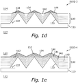
- Figure 1d illustrates schematically yet another different, alternative step S102-3 in an alternative embodiment of the method.
- the epitaxial growth process is here the same as that described with reference to Figure 1c (i.e. using the second set of growth rates), but the epitaxial growth is continued until the (complete) thickness of the epitaxial layer 130 is approximately 3 ⁇ m.
- the angles 122 and 132 remain the same, but it may be seen that there no longer remains any (111) face on the surface 134 of the epitaxial layer 130.
- Figure 1e illustrates schematically yet another different, alternative step S102-4 in an alternative embodiment of the method.
- the epitaxial growth process is here the same as that described with reference to Figure 1b (i.e. using the first set of growth rates), but the epitaxial growth is continued until the (complete) thickness of the epitaxial layer 130 is approximately 3 ⁇ m.
- the angles 122 and 132 remain the same, but it may be seen that an additional face 146, for example a (911) face, having an angle 133 of approximately 9° (or 8.93°) also forms as an additional face of the layer 130.
- the normalized growth ratios (with respect to the (100) face) for such a 911 face may, using the first set of parameters, be for example 0.27.
- the at least one epitaxial layer may have several facets, where the slope angle of a facet with respect to the substrate changes abruptly when moving from one facet to a neighboring facet.
- This is illustrated e.g. in the examples of embodiments provided with reference to Figures 1a-1e .
- the examples provide examples of specific faces, such as the (111), (311) and (911) with respect to the (100) face, it is envisaged of course also that other faces, such as e.g. a (1211, twelve-one-one) face may be present in addition, or as alternatives, as long as the angles at the top of the pyramids belong to the desired intervals as specified herein with regards to e.g. optimal light trapping.
- a (1211) face may for example corresponding to an angle of approximately 7° (or 6.72°).
- the epitaxial growth process may include for example a temperature between 700 - 1000 °C, a pressure between 10 - 1000 Torr, a growth rate between 5 - 500 nm/min, SiH 2 Cl 2 as a silicon source, and B 2 H 6 as a dopant source.
- a gas flow ratio (as measured e.g. by a gas flow controller) of dopant source to silicon source may for example be between 10 -5 to 10 -2 , while a gas flow ratio of carrier gas to silicon source may for example be between 200 to 500. It may here be envisaged that, when discussing gas flow ratios, it is assumed that a concentration of the precursors is normalized to 100%.
- the silicon source may be SiHCl 3 or SiH 4 , the temperature range 900 - 1150 °C, and the growth rate range 200 - 4000 nm/min.
- Dopant sources may include for example B 2 H 6 and BCl 3 , which may create a p-type epitaxial layer.
- Other dopant sources envisaged includes for example PH 3 and AsH 3 , which may create an n-type epitaxial layer.
- the growth rate ratios may correspond to those in the first set of growth rates.
- the growth rate ratios may correspond to those in the second set of growth rates, as described above.
- the epitaxial growth of the (at least one) epitaxial layer may be performed only at the rear side of the substrate and not at the front side.
- the front side may e.g. then retain its original pyramidal topography for light trapping purposes.
- Such a "selective" epitaxial deposition (with respect to the front/rear side of the substrate) may be obtained using process conditions which are selected to avoid parasitic deposition on the front side, e.g. by avoiding the use of SiH 4 as a silicon precursor. Instead, using e.g. SiH 2 Cl 2 or SiHCl 3 as silicon precursors (as described earlier herein) may allow for such selective epitaxial growth/deposition.
- the present disclosure suggests also to design the doping level of the doped layer in accordance with the sheet resistance value, as the solar cell device requires.
- the optical gain provided by the method of the present disclosure may be valid for various device structures, including e.g. nPERT (n-type passivated emitter, rear totally diffused) p+ rear emitter structures, pPERT (p-type passivated emitter, rear totally diffused) p+ rear back surface field (BSF) structures, and nPERT n+ BSF structures.
- the thickness of the epitaxial layer may be between 1-3 ⁇ m, a sheet resistance may correspond to 50 - 250 ⁇ /sq and a (Boron) doping level range may correspond to 2 ⁇ 10 17 - 2 ⁇ 10 19 cm -3 .
- the thickness of the epitaxial layer may be between 1-3 ⁇ m, a sheet resistance may correspond to 50 - 350 ⁇ /sq and a (Boron) doping level range may correspond to 2 ⁇ 10 17 - 2 ⁇ 10 19 cm -3 .
- the present disclosure also provides a crystalline silicon bifacial solar cell.
- the solar cell may correspond to e.g. one of the structures shown in and described with reference to any of Figures 1b-1c .
- the solar cell may include a silicon substrate 110 having a front side 112 and a rear side 114.
- the rear side 114 may be patterned with pyramids 120, and at least one smoothing layer 130 of epitaxially grown silicon may be provided on the pyramids 120.
- a pyramid angle 122 of the pyramids 120 may be at least 40° (such as for example 54.7°).
- an angle 132 between a surface 134 of the at least one smoothing layer 130 and the substrate 110 may be between 5 to 35°.
- the angle 132 may be between 10 to 25°, preferably 20°.
- a solar cell according to the present disclosure may be identified by the presence of sharp transitions between different facets, i.e. sharp transitions between different angles, of the epitaxial smoothing layer.
- a common solar cell wherein smoothing of the pyramidal topology has been obtained by e.g. wet chemical processing may instead be identified by there, instead, being a smooth transition between different angles and no distinct facets.
- the present disclosure provides an improved way of simultaneously, in e.g. a same processing step, both a) form a doped layer (e.g. a junction) on the rear side of a crystalline silicon bifacial solar cell, and b) to use the formed doped layer to smooth a pyramidal textured surface of the rear side in order to obtain sufficient surface passivation.
- the thickness of the epitaxial doped layer (and the corresponding angle of the epitaxial layer at the top of the pyramids) may be tailored to obtain both an optimal light generated current density and a layer depth allowing for a sufficiently low doping level of the doped layer (junction) to limit Auger recombination losses.
Landscapes
- Photovoltaic Devices (AREA)
- Chemical & Material Sciences (AREA)
- Crystallography & Structural Chemistry (AREA)
Priority Applications (3)
| Application Number | Priority Date | Filing Date | Title |
|---|---|---|---|
| EP18214806.4A EP3671863B1 (fr) | 2018-12-20 | 2018-12-20 | Couche dopée arrière lissée pour une cellule solaire biface |
| US16/714,477 US11075317B2 (en) | 2018-12-20 | 2019-12-13 | Smoothed doped layer for solar cell |
| CN201911294280.0A CN111430501B (zh) | 2018-12-20 | 2019-12-16 | 双面太阳能电池的平滑后侧掺杂层 |
Applications Claiming Priority (1)
| Application Number | Priority Date | Filing Date | Title |
|---|---|---|---|
| EP18214806.4A EP3671863B1 (fr) | 2018-12-20 | 2018-12-20 | Couche dopée arrière lissée pour une cellule solaire biface |
Publications (2)
| Publication Number | Publication Date |
|---|---|
| EP3671863A1 true EP3671863A1 (fr) | 2020-06-24 |
| EP3671863B1 EP3671863B1 (fr) | 2021-06-09 |
Family
ID=64755259
Family Applications (1)
| Application Number | Title | Priority Date | Filing Date |
|---|---|---|---|
| EP18214806.4A Active EP3671863B1 (fr) | 2018-12-20 | 2018-12-20 | Couche dopée arrière lissée pour une cellule solaire biface |
Country Status (3)
| Country | Link |
|---|---|
| US (1) | US11075317B2 (fr) |
| EP (1) | EP3671863B1 (fr) |
| CN (1) | CN111430501B (fr) |
Families Citing this family (1)
| Publication number | Priority date | Publication date | Assignee | Title |
|---|---|---|---|---|
| CN118782663B (zh) * | 2024-09-12 | 2024-12-06 | 通威太阳能(成都)有限公司 | 太阳电池及光伏组件 |
Citations (4)
| Publication number | Priority date | Publication date | Assignee | Title |
|---|---|---|---|---|
| EP1973167A2 (fr) * | 2007-03-19 | 2008-09-24 | Sanyo Electric Co., Ltd. | Dispositif photovoltaïque et son procédé de fabrication |
| EP2479797A1 (fr) * | 2009-09-18 | 2012-07-25 | Sanyo Electric Co., Ltd. | Batterie solaire, module de batterie solaire, et système de batterie solaire |
| US20130288418A1 (en) * | 2008-11-13 | 2013-10-31 | Solexel, Inc. | Method for fabricating a three-dimensional thin-film semiconductor substrate from a template |
| US20180315866A1 (en) * | 2017-04-26 | 2018-11-01 | Lg Electronics Inc. | Solar cell and method of manufacturing the same |
Family Cites Families (13)
| Publication number | Priority date | Publication date | Assignee | Title |
|---|---|---|---|---|
| JP2003069061A (ja) * | 2001-08-24 | 2003-03-07 | Sharp Corp | 積層型光電変換素子 |
| US8420435B2 (en) * | 2009-05-05 | 2013-04-16 | Solexel, Inc. | Ion implantation fabrication process for thin-film crystalline silicon solar cells |
| US8759138B2 (en) * | 2008-02-11 | 2014-06-24 | Suncore Photovoltaics, Inc. | Concentrated photovoltaic system modules using III-V semiconductor solar cells |
| NL2003390C2 (en) * | 2009-08-25 | 2011-02-28 | Stichting Energie | Solar cell and method for manufacturing such a solar cell. |
| DE102010024309A1 (de) * | 2010-06-18 | 2011-12-22 | Fraunhofer-Gesellschaft zur Förderung der angewandten Forschung e.V. | Verfahren zur Herstellung einer photovoltaischen Solarzelle |
| US8486746B2 (en) * | 2011-03-29 | 2013-07-16 | Sunpower Corporation | Thin silicon solar cell and method of manufacture |
| GB2502293A (en) * | 2012-05-22 | 2013-11-27 | Renewable Energy Corp Asa | A method for manufacturing a back contacted back junction solar cell module |
| CN104350607B (zh) * | 2012-06-13 | 2018-01-12 | 三菱电机株式会社 | 太阳能电池及其制造方法 |
| GB2524699C (en) * | 2013-02-07 | 2018-11-14 | Wood John | A bipolar junction transistor structure |
| JP2016532317A (ja) * | 2013-09-27 | 2016-10-13 | ダンマークス テクニスク ユニバーシテットDanmarks Tekniske Universitet | ナノ構造化されたシリコン系太陽電池およびナノ構造化されたシリコン系太陽電池を製造する方法 |
| EP3331029B1 (fr) * | 2016-12-02 | 2021-09-01 | LG Electronics Inc. | Cellule solaire en tandem et son procédé de fabrication |
| CN110476256B (zh) * | 2017-03-31 | 2023-02-28 | 株式会社钟化 | 太阳能电池、太阳能电池模块和太阳能电池的制造方法 |
| EP3404724B1 (fr) * | 2017-05-19 | 2022-08-03 | LG Electronics Inc. | Cellule solaire et son procédé de fabrication |
-
2018
- 2018-12-20 EP EP18214806.4A patent/EP3671863B1/fr active Active
-
2019
- 2019-12-13 US US16/714,477 patent/US11075317B2/en active Active
- 2019-12-16 CN CN201911294280.0A patent/CN111430501B/zh active Active
Patent Citations (4)
| Publication number | Priority date | Publication date | Assignee | Title |
|---|---|---|---|---|
| EP1973167A2 (fr) * | 2007-03-19 | 2008-09-24 | Sanyo Electric Co., Ltd. | Dispositif photovoltaïque et son procédé de fabrication |
| US20130288418A1 (en) * | 2008-11-13 | 2013-10-31 | Solexel, Inc. | Method for fabricating a three-dimensional thin-film semiconductor substrate from a template |
| EP2479797A1 (fr) * | 2009-09-18 | 2012-07-25 | Sanyo Electric Co., Ltd. | Batterie solaire, module de batterie solaire, et système de batterie solaire |
| US20180315866A1 (en) * | 2017-04-26 | 2018-11-01 | Lg Electronics Inc. | Solar cell and method of manufacturing the same |
Non-Patent Citations (2)
| Title |
|---|
| MCINTOSH KEITH R ET AL: "Optical Evaluation of Silicon Wafers With Rounded Rear Pyramids", IEEE JOURNAL OF PHOTOVOLTAICS, I E E E, US, vol. 7, no. 6, November 2017 (2017-11-01), pages 1596 - 1602, XP011672041, ISSN: 2156-3381, [retrieved on 20171023], DOI: 10.1109/JPHOTOV.2017.2754060 * |
| MOEHLECKE A ET AL: "PRACTICAL HIGH EFFICIENCY BIFACIAL SOLAR CELLS", WORLD CONFERENCE ON PHOTOVOLTAIC ENERGY. WAIKOLOA, DEC. 5 - 9, 1994; [WORLD CONFERENCE ON PHOTOVOLTAIC ENERGY], NEW YORK, IEEE, US, vol. CONF. 1, 5 December 1994 (1994-12-05), pages 1663 - 1666, XP000680133, ISBN: 978-0-7803-1460-3, DOI: 10.1109/WCPEC.1994.520538 * |
Also Published As
| Publication number | Publication date |
|---|---|
| CN111430501B (zh) | 2024-07-02 |
| US11075317B2 (en) | 2021-07-27 |
| US20200203553A1 (en) | 2020-06-25 |
| CN111430501A (zh) | 2020-07-17 |
| EP3671863B1 (fr) | 2021-06-09 |
Similar Documents
| Publication | Publication Date | Title |
|---|---|---|
| JP5374504B2 (ja) | エミッタ構造の作製方法とその結果のエミッタ構造 | |
| US20100108130A1 (en) | Thin Interdigitated backside contact solar cell and manufacturing process thereof | |
| US8859888B2 (en) | Solar cell with nanostructured layer and methods of making and using | |
| US20130330872A1 (en) | Ion implantation fabrication process for thin-film crystalline silicon solar cells | |
| US11335822B2 (en) | Multijunction solar cell having patterned emitter and method of making the solar cell | |
| EP2740149B1 (fr) | Procédé de formation de motifs de régions dopées de manière différente | |
| CN102165606A (zh) | 抑制具有异质结的光电器件中外延生长的方法和光电器件 | |
| CN113948607A (zh) | 一种用于制备n型选择性发射极晶硅电池的选择性扩散方法及其应用 | |
| CN117423762A (zh) | 太阳电池及其制备方法、光伏组件、光伏系统 | |
| US11075317B2 (en) | Smoothed doped layer for solar cell | |
| JP6652795B2 (ja) | 結晶太陽電池の製造方法 | |
| Hao et al. | High efficiency solar cells on direct kerfless 156 mm mono crystalline Si wafers by high throughput epitaxial growth | |
| CN101937941B (zh) | 一种晶体硅太阳电池选择性发射结的制作方法 | |
| JP4325912B2 (ja) | 太陽電池素子及びその製造方法 | |
| US20100236617A1 (en) | Stacked Structure Solar Cell Having Backside Conductive Contacts | |
| CN212230440U (zh) | 单晶电池片及光伏组件 | |
| KR102042267B1 (ko) | 태양 전지 및 이의 제조 방법 | |
| KR101024322B1 (ko) | 태양전지용 웨이퍼 제조 방법, 그 방법으로 제조된 태양전지용 웨이퍼 및 이를 이용한 태양전지 제조 방법 | |
| JP2018142703A (ja) | 太陽電池及びその製造方法 | |
| JP2014154619A (ja) | 光電変換素子の製造方法 | |
| Lamers et al. | Towards 21% efficient N-CZ IBC based on screen printing | |
| EP3179522A1 (fr) | Procédé de fabrication de dispositifs photovoltaïques à contact arrière interdigité | |
| CN201796899U (zh) | 一种单深结密栅线结构太阳电池 | |
| JP2001168356A (ja) | 太陽電池セルの製造方法 | |
| CN102714253A (zh) | 具有长条形孔的外延穿孔卷绕式太阳能电池及其制造方法 |
Legal Events
| Date | Code | Title | Description |
|---|---|---|---|
| PUAI | Public reference made under article 153(3) epc to a published international application that has entered the european phase |
Free format text: ORIGINAL CODE: 0009012 |
|
| STAA | Information on the status of an ep patent application or granted ep patent |
Free format text: STATUS: THE APPLICATION HAS BEEN PUBLISHED |
|
| AK | Designated contracting states |
Kind code of ref document: A1 Designated state(s): AL AT BE BG CH CY CZ DE DK EE ES FI FR GB GR HR HU IE IS IT LI LT LU LV MC MK MT NL NO PL PT RO RS SE SI SK SM TR |
|
| AX | Request for extension of the european patent |
Extension state: BA ME |
|
| STAA | Information on the status of an ep patent application or granted ep patent |
Free format text: STATUS: REQUEST FOR EXAMINATION WAS MADE |
|
| 17P | Request for examination filed |
Effective date: 20201217 |
|
| RBV | Designated contracting states (corrected) |
Designated state(s): AL AT BE BG CH CY CZ DE DK EE ES FI FR GB GR HR HU IE IS IT LI LT LU LV MC MK MT NL NO PL PT RO RS SE SI SK SM TR |
|
| GRAP | Despatch of communication of intention to grant a patent |
Free format text: ORIGINAL CODE: EPIDOSNIGR1 |
|
| STAA | Information on the status of an ep patent application or granted ep patent |
Free format text: STATUS: GRANT OF PATENT IS INTENDED |
|
| INTG | Intention to grant announced |
Effective date: 20210218 |
|
| GRAS | Grant fee paid |
Free format text: ORIGINAL CODE: EPIDOSNIGR3 |
|
| GRAA | (expected) grant |
Free format text: ORIGINAL CODE: 0009210 |
|
| STAA | Information on the status of an ep patent application or granted ep patent |
Free format text: STATUS: THE PATENT HAS BEEN GRANTED |
|
| AK | Designated contracting states |
Kind code of ref document: B1 Designated state(s): AL AT BE BG CH CY CZ DE DK EE ES FI FR GB GR HR HU IE IS IT LI LT LU LV MC MK MT NL NO PL PT RO RS SE SI SK SM TR |
|
| REG | Reference to a national code |
Ref country code: GB Ref legal event code: FG4D |
|
| REG | Reference to a national code |
Ref country code: CH Ref legal event code: EP Ref country code: AT Ref legal event code: REF Ref document number: 1401200 Country of ref document: AT Kind code of ref document: T Effective date: 20210615 |
|
| REG | Reference to a national code |
Ref country code: DE Ref legal event code: R096 Ref document number: 602018018329 Country of ref document: DE |
|
| REG | Reference to a national code |
Ref country code: IE Ref legal event code: FG4D |
|
| REG | Reference to a national code |
Ref country code: LT Ref legal event code: MG9D |
|
| PG25 | Lapsed in a contracting state [announced via postgrant information from national office to epo] |
Ref country code: BG Free format text: LAPSE BECAUSE OF FAILURE TO SUBMIT A TRANSLATION OF THE DESCRIPTION OR TO PAY THE FEE WITHIN THE PRESCRIBED TIME-LIMIT Effective date: 20210909 Ref country code: FI Free format text: LAPSE BECAUSE OF FAILURE TO SUBMIT A TRANSLATION OF THE DESCRIPTION OR TO PAY THE FEE WITHIN THE PRESCRIBED TIME-LIMIT Effective date: 20210609 Ref country code: LT Free format text: LAPSE BECAUSE OF FAILURE TO SUBMIT A TRANSLATION OF THE DESCRIPTION OR TO PAY THE FEE WITHIN THE PRESCRIBED TIME-LIMIT Effective date: 20210609 Ref country code: HR Free format text: LAPSE BECAUSE OF FAILURE TO SUBMIT A TRANSLATION OF THE DESCRIPTION OR TO PAY THE FEE WITHIN THE PRESCRIBED TIME-LIMIT Effective date: 20210609 |
|
| REG | Reference to a national code |
Ref country code: AT Ref legal event code: MK05 Ref document number: 1401200 Country of ref document: AT Kind code of ref document: T Effective date: 20210609 |
|
| REG | Reference to a national code |
Ref country code: NL Ref legal event code: MP Effective date: 20210609 |
|
| PG25 | Lapsed in a contracting state [announced via postgrant information from national office to epo] |
Ref country code: GR Free format text: LAPSE BECAUSE OF FAILURE TO SUBMIT A TRANSLATION OF THE DESCRIPTION OR TO PAY THE FEE WITHIN THE PRESCRIBED TIME-LIMIT Effective date: 20210910 Ref country code: NO Free format text: LAPSE BECAUSE OF FAILURE TO SUBMIT A TRANSLATION OF THE DESCRIPTION OR TO PAY THE FEE WITHIN THE PRESCRIBED TIME-LIMIT Effective date: 20210909 Ref country code: LV Free format text: LAPSE BECAUSE OF FAILURE TO SUBMIT A TRANSLATION OF THE DESCRIPTION OR TO PAY THE FEE WITHIN THE PRESCRIBED TIME-LIMIT Effective date: 20210609 Ref country code: SE Free format text: LAPSE BECAUSE OF FAILURE TO SUBMIT A TRANSLATION OF THE DESCRIPTION OR TO PAY THE FEE WITHIN THE PRESCRIBED TIME-LIMIT Effective date: 20210609 Ref country code: RS Free format text: LAPSE BECAUSE OF FAILURE TO SUBMIT A TRANSLATION OF THE DESCRIPTION OR TO PAY THE FEE WITHIN THE PRESCRIBED TIME-LIMIT Effective date: 20210609 |
|
| PG25 | Lapsed in a contracting state [announced via postgrant information from national office to epo] |
Ref country code: SK Free format text: LAPSE BECAUSE OF FAILURE TO SUBMIT A TRANSLATION OF THE DESCRIPTION OR TO PAY THE FEE WITHIN THE PRESCRIBED TIME-LIMIT Effective date: 20210609 Ref country code: SM Free format text: LAPSE BECAUSE OF FAILURE TO SUBMIT A TRANSLATION OF THE DESCRIPTION OR TO PAY THE FEE WITHIN THE PRESCRIBED TIME-LIMIT Effective date: 20210609 Ref country code: ES Free format text: LAPSE BECAUSE OF FAILURE TO SUBMIT A TRANSLATION OF THE DESCRIPTION OR TO PAY THE FEE WITHIN THE PRESCRIBED TIME-LIMIT Effective date: 20210609 Ref country code: EE Free format text: LAPSE BECAUSE OF FAILURE TO SUBMIT A TRANSLATION OF THE DESCRIPTION OR TO PAY THE FEE WITHIN THE PRESCRIBED TIME-LIMIT Effective date: 20210609 Ref country code: PT Free format text: LAPSE BECAUSE OF FAILURE TO SUBMIT A TRANSLATION OF THE DESCRIPTION OR TO PAY THE FEE WITHIN THE PRESCRIBED TIME-LIMIT Effective date: 20211011 Ref country code: RO Free format text: LAPSE BECAUSE OF FAILURE TO SUBMIT A TRANSLATION OF THE DESCRIPTION OR TO PAY THE FEE WITHIN THE PRESCRIBED TIME-LIMIT Effective date: 20210609 Ref country code: NL Free format text: LAPSE BECAUSE OF FAILURE TO SUBMIT A TRANSLATION OF THE DESCRIPTION OR TO PAY THE FEE WITHIN THE PRESCRIBED TIME-LIMIT Effective date: 20210609 Ref country code: CZ Free format text: LAPSE BECAUSE OF FAILURE TO SUBMIT A TRANSLATION OF THE DESCRIPTION OR TO PAY THE FEE WITHIN THE PRESCRIBED TIME-LIMIT Effective date: 20210609 Ref country code: AT Free format text: LAPSE BECAUSE OF FAILURE TO SUBMIT A TRANSLATION OF THE DESCRIPTION OR TO PAY THE FEE WITHIN THE PRESCRIBED TIME-LIMIT Effective date: 20210609 |
|
| PG25 | Lapsed in a contracting state [announced via postgrant information from national office to epo] |
Ref country code: PL Free format text: LAPSE BECAUSE OF FAILURE TO SUBMIT A TRANSLATION OF THE DESCRIPTION OR TO PAY THE FEE WITHIN THE PRESCRIBED TIME-LIMIT Effective date: 20210609 |
|
| REG | Reference to a national code |
Ref country code: DE Ref legal event code: R097 Ref document number: 602018018329 Country of ref document: DE |
|
| PLBE | No opposition filed within time limit |
Free format text: ORIGINAL CODE: 0009261 |
|
| STAA | Information on the status of an ep patent application or granted ep patent |
Free format text: STATUS: NO OPPOSITION FILED WITHIN TIME LIMIT |
|
| PG25 | Lapsed in a contracting state [announced via postgrant information from national office to epo] |
Ref country code: DK Free format text: LAPSE BECAUSE OF FAILURE TO SUBMIT A TRANSLATION OF THE DESCRIPTION OR TO PAY THE FEE WITHIN THE PRESCRIBED TIME-LIMIT Effective date: 20210609 |
|
| 26N | No opposition filed |
Effective date: 20220310 |
|
| PG25 | Lapsed in a contracting state [announced via postgrant information from national office to epo] |
Ref country code: AL Free format text: LAPSE BECAUSE OF FAILURE TO SUBMIT A TRANSLATION OF THE DESCRIPTION OR TO PAY THE FEE WITHIN THE PRESCRIBED TIME-LIMIT Effective date: 20210609 |
|
| PG25 | Lapsed in a contracting state [announced via postgrant information from national office to epo] |
Ref country code: MC Free format text: LAPSE BECAUSE OF FAILURE TO SUBMIT A TRANSLATION OF THE DESCRIPTION OR TO PAY THE FEE WITHIN THE PRESCRIBED TIME-LIMIT Effective date: 20210609 Ref country code: IT Free format text: LAPSE BECAUSE OF FAILURE TO SUBMIT A TRANSLATION OF THE DESCRIPTION OR TO PAY THE FEE WITHIN THE PRESCRIBED TIME-LIMIT Effective date: 20210609 |
|
| REG | Reference to a national code |
Ref country code: CH Ref legal event code: PL |
|
| REG | Reference to a national code |
Ref country code: BE Ref legal event code: MM Effective date: 20211231 |
|
| PG25 | Lapsed in a contracting state [announced via postgrant information from national office to epo] |
Ref country code: LU Free format text: LAPSE BECAUSE OF NON-PAYMENT OF DUE FEES Effective date: 20211220 Ref country code: IE Free format text: LAPSE BECAUSE OF NON-PAYMENT OF DUE FEES Effective date: 20211220 |
|
| PG25 | Lapsed in a contracting state [announced via postgrant information from national office to epo] |
Ref country code: BE Free format text: LAPSE BECAUSE OF NON-PAYMENT OF DUE FEES Effective date: 20211231 |
|
| PG25 | Lapsed in a contracting state [announced via postgrant information from national office to epo] |
Ref country code: LI Free format text: LAPSE BECAUSE OF NON-PAYMENT OF DUE FEES Effective date: 20211231 Ref country code: CH Free format text: LAPSE BECAUSE OF NON-PAYMENT OF DUE FEES Effective date: 20211231 |
|
| P01 | Opt-out of the competence of the unified patent court (upc) registered |
Effective date: 20230513 |
|
| PG25 | Lapsed in a contracting state [announced via postgrant information from national office to epo] |
Ref country code: CY Free format text: LAPSE BECAUSE OF FAILURE TO SUBMIT A TRANSLATION OF THE DESCRIPTION OR TO PAY THE FEE WITHIN THE PRESCRIBED TIME-LIMIT Effective date: 20210609 |
|
| PG25 | Lapsed in a contracting state [announced via postgrant information from national office to epo] |
Ref country code: HU Free format text: LAPSE BECAUSE OF FAILURE TO SUBMIT A TRANSLATION OF THE DESCRIPTION OR TO PAY THE FEE WITHIN THE PRESCRIBED TIME-LIMIT; INVALID AB INITIO Effective date: 20181220 |
|
| GBPC | Gb: european patent ceased through non-payment of renewal fee |
Effective date: 20221220 |
|
| PG25 | Lapsed in a contracting state [announced via postgrant information from national office to epo] |
Ref country code: GB Free format text: LAPSE BECAUSE OF NON-PAYMENT OF DUE FEES Effective date: 20221220 |
|
| PG25 | Lapsed in a contracting state [announced via postgrant information from national office to epo] |
Ref country code: MK Free format text: LAPSE BECAUSE OF FAILURE TO SUBMIT A TRANSLATION OF THE DESCRIPTION OR TO PAY THE FEE WITHIN THE PRESCRIBED TIME-LIMIT Effective date: 20210609 |
|
| PG25 | Lapsed in a contracting state [announced via postgrant information from national office to epo] |
Ref country code: MT Free format text: LAPSE BECAUSE OF FAILURE TO SUBMIT A TRANSLATION OF THE DESCRIPTION OR TO PAY THE FEE WITHIN THE PRESCRIBED TIME-LIMIT Effective date: 20210609 |
|
| REG | Reference to a national code |
Ref country code: DE Ref legal event code: R079 Ref document number: 602018018329 Country of ref document: DE Free format text: PREVIOUS MAIN CLASS: H01L0031023600 Ipc: H10F0077700000 |
|
| PG25 | Lapsed in a contracting state [announced via postgrant information from national office to epo] |
Ref country code: TR Free format text: LAPSE BECAUSE OF FAILURE TO SUBMIT A TRANSLATION OF THE DESCRIPTION OR TO PAY THE FEE WITHIN THE PRESCRIBED TIME-LIMIT Effective date: 20210609 |
|
| PGFP | Annual fee paid to national office [announced via postgrant information from national office to epo] |
Ref country code: DE Payment date: 20251126 Year of fee payment: 8 |
|
| PGFP | Annual fee paid to national office [announced via postgrant information from national office to epo] |
Ref country code: FR Payment date: 20251120 Year of fee payment: 8 |