EP3671867A1 - Structure de ruban pour ensemble pile - Google Patents
Structure de ruban pour ensemble pile Download PDFInfo
- Publication number
- EP3671867A1 EP3671867A1 EP17924556.8A EP17924556A EP3671867A1 EP 3671867 A1 EP3671867 A1 EP 3671867A1 EP 17924556 A EP17924556 A EP 17924556A EP 3671867 A1 EP3671867 A1 EP 3671867A1
- Authority
- EP
- European Patent Office
- Prior art keywords
- cell slice
- grid lines
- slice
- fine grid
- connecting portion
- Prior art date
- Legal status (The legal status is an assumption and is not a legal conclusion. Google has not performed a legal analysis and makes no representation as to the accuracy of the status listed.)
- Granted
Links
Images



Classifications
-
- H—ELECTRICITY
- H10—SEMICONDUCTOR DEVICES; ELECTRIC SOLID-STATE DEVICES NOT OTHERWISE PROVIDED FOR
- H10F—INORGANIC SEMICONDUCTOR DEVICES SENSITIVE TO INFRARED RADIATION, LIGHT, ELECTROMAGNETIC RADIATION OF SHORTER WAVELENGTH OR CORPUSCULAR RADIATION
- H10F19/00—Integrated devices, or assemblies of multiple devices, comprising at least one photovoltaic cell covered by group H10F10/00, e.g. photovoltaic modules
- H10F19/90—Structures for connecting between photovoltaic cells, e.g. interconnections or insulating spacers
- H10F19/902—Structures for connecting between photovoltaic cells, e.g. interconnections or insulating spacers for series or parallel connection of photovoltaic cells
- H10F19/906—Structures for connecting between photovoltaic cells, e.g. interconnections or insulating spacers for series or parallel connection of photovoltaic cells characterised by the materials of the structures
-
- H—ELECTRICITY
- H10—SEMICONDUCTOR DEVICES; ELECTRIC SOLID-STATE DEVICES NOT OTHERWISE PROVIDED FOR
- H10F—INORGANIC SEMICONDUCTOR DEVICES SENSITIVE TO INFRARED RADIATION, LIGHT, ELECTROMAGNETIC RADIATION OF SHORTER WAVELENGTH OR CORPUSCULAR RADIATION
- H10F19/00—Integrated devices, or assemblies of multiple devices, comprising at least one photovoltaic cell covered by group H10F10/00, e.g. photovoltaic modules
- H10F19/90—Structures for connecting between photovoltaic cells, e.g. interconnections or insulating spacers
- H10F19/902—Structures for connecting between photovoltaic cells, e.g. interconnections or insulating spacers for series or parallel connection of photovoltaic cells
- H10F19/904—Structures for connecting between photovoltaic cells, e.g. interconnections or insulating spacers for series or parallel connection of photovoltaic cells characterised by the shapes of the structures
-
- Y—GENERAL TAGGING OF NEW TECHNOLOGICAL DEVELOPMENTS; GENERAL TAGGING OF CROSS-SECTIONAL TECHNOLOGIES SPANNING OVER SEVERAL SECTIONS OF THE IPC; TECHNICAL SUBJECTS COVERED BY FORMER USPC CROSS-REFERENCE ART COLLECTIONS [XRACs] AND DIGESTS
- Y02—TECHNOLOGIES OR APPLICATIONS FOR MITIGATION OR ADAPTATION AGAINST CLIMATE CHANGE
- Y02E—REDUCTION OF GREENHOUSE GAS [GHG] EMISSIONS, RELATED TO ENERGY GENERATION, TRANSMISSION OR DISTRIBUTION
- Y02E10/00—Energy generation through renewable energy sources
- Y02E10/50—Photovoltaic [PV] energy
Definitions
- the disclosure belongs to the field of photovoltaic module technologies, and more particularly, relates to a solder strip applied to a shingled solar cell module.
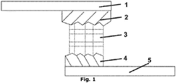
- a shingled solar cell module is generally constructed by cutting a solar cell with a size of 156.75mm ⁇ 156.75mm into small cell slices along a direction parallel to busbars, and arranging the small cell slices in series-parallel connection through conductive adhesive, which is as shown in FIG. 1 .
- An internal area of the shingled solar cell module can be sufficiently utilized, and under the same area, the shingled solar cell module can accommodate more cell slice than a common module by 13%.
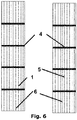
- Two aspects need to be considered for the shingled solar cell module: one aspect is that the automation of connecting the cell slices by the conductive adhesive is difficult; and the second aspect is that a current between cell slice is mainly collected through fine grid lines. As shown in FIG. 2 , once the fine grid lines are fractured, a series resistance will be increased, thus increasing a power loss, especially in the case where adjacent fine grid lines are fractured.
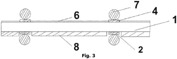
- the MBB or Smartwire technology mainly solders 10 to 18 pieces of round solder strips having a diameter of about 300 ⁇ m with grid lines, of which the MBB technology mainly solders round solder strips 7 in parallel with busbars and the Smartwire technology mainly solders the round solder strips 7 perpendicularly to fine grid lines 6. As shown in FIGS.
- FIG. 5 is a soldering schematic diagram when the current Smartwire technology is combined with a shingled solar cell module.
- the main difficulty to apply the MBB or Smartwire technology to the shingled solar cell technology is that cell slices 1 are connected in series by the round solder strips 7, which will generate a large stress point at a soldering point in loading and temperature cycling tests, and are prone to cracking and other problems.
- the disclosure is intended to provide a solder strip applied to a shingled solar cell module, so as to solve one or more of the problems of difficult serial soldering of the shingled solar cell module: the first problem is that the automatic serial soldering requirement of the shingled solar cell module at current is high when the conductive adhesive is used for series connection, which cannot satisfy the required capacity for fast serial soldering; the second problem is more cracks under loading and temperature stresses generated when the MBB or Smartwire technology is combined with the shingled solar cell module; and the third problem is the power loss caused by the fine grid fracture of the shingled solar cell module.
- a solder strip applied to a shingled solar cell module includes a flat portion, and an upper cell slice connecting portion, and a lower cell slice connecting portion located at two sides of the flat portion; wherein, the solder strip is used for connecting a lower cell slice and an upper cell slice which form the shingled solar cell module; the shingled solar cell module is formed by solar cells without bus bar; a plurality of fine grid lines are arranged in parallel on a front surface of the lower cell slice, and a plurality of fine grid lines are arranged in parallel on a back surface of the upper cell slice; the fine grid lines on the front surface of the lower cell slice and the fine grid lines on the back surface of the upper cell slice are arranged in parallel; cutting directions of the lower cell slice and the upper cell slice are parallel to the fine grid lines; the solder strip is arranged perpendicular to the fine grid lines; and the upper cell slice partially overlaps the lower cell slice, the flat portion is soldered to the fine grid lines on the front surface of the lower cell slice and the fine grid lines on the back surface of
- the upper cell slice connecting portion is in a shape of a round bar.
- the lower cell slice connecting portion is in a shape of a round bar.
- the flat portion is made of a round bar by stamping.
- a solder strip applied to a shingled solar cell module includes a flat portion, and an upper cell slice connecting portion and a lower cell slice connecting portion located at two sides of the flat portion; wherein, the solder strip is used for connecting a lower cell slice and an upper cell slice which form the shingled solar cell module; the shingled solar cell module is formed by multi-busbar solar cells; a plurality of fine grid lines are arranged in parallel on a front surface of the lower cell slice, and a plurality of fine grid lines are arranged in parallel on a back surface of the upper cell slice; the fine grid lines on the front surface of the lower cell slice and the fine grid lines on the back surface of the upper cell slice are arranged in parallel; cutting directions of the lower cell slice and the upper cell slice are parallel to the fine grid lines; a plurality of busbars are further perpendicularly arranged on the plurality of fine grid lines on the front surface of the lower cell slice, and a plurality of busbars are further arranged on the plurality of fine grid lines on the back surface
- the upper cell slice connecting portion is in a shape of a round bar.
- the flat portion is made of a round bar by stamping.
- a solder strip applied to a shingled solar cell module includes a flat portion, and an upper cell slice connecting portion and a lower cell slice connecting portion located at two sides of the flat portion, wherein the upper cell slice connecting portion and the lower cell slice connecting portion have a thickness greater than that of the flat portion.
- 1 refers to upper cell slice
- 2 refers to busbars on the back surface of the cell slice
- 3 refers to conductive adhesive
- 4 refers to busbars on the front surface of the cell slice
- 5 refers to lower cell slice
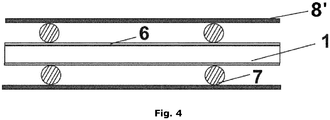
- 6 refers to fine grid lines
- 7 refers to round solder strip
- 8 refers to aluminum back surface field
- 8' refers to a transparent polymer
- 9 refers to flat portion
- 10 refers to upper cell slice connecting portion
- 11 refers to lower cell slice connecting portion.
- a round solder strip 7 is round having a size of about 300 ⁇ m, and is bonded to a cell slice through a transparent polymer film 8' that servers as a carrier, as shown in FIG. 4 .
- the solder strip is perpendicularly soldered to fine grid lines 6 via pressure and temperature to form excellent electrical properties.
- a Smartwire technology is applied to a shingled solar cell technology, it is necessary to adjust a direction of the fine grid lines 6 so that the fine grid lines 6 are perpendicular to a direction of the solder strip.
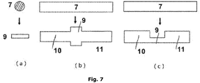
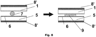
- the disclosure provides a solder strip applied to a shingled solar cell module, which adds a stamping step to a round solder strip 7 used by Smartwire technology in a series soldering process, so that the solder strip at the shingled solar cell is changed from round to rectangular to form a flat portion 9 (as shown in FIGS. 7(a) to 7(c) ), thus greatly increasing a contact area between the solder strip and a cell slice, and reducing a crack risk of the solder strip, as shown in FIGS. 8 and 9 .
- the solder strip may also play a role of current collection, which greatly reduces a power loss caused by grid fracture.
- a Smartwire solder strip in a light-facing area of the cell is round, which can reutilize light intensity to increase the power of the module.
- the solder strip applied to a shingled solar cell module includes a flat portion 9, an upper cell slice connecting portion 10 in a shape of a round bar and a lower cell slice connecting portion 11 in a shape of a round bar, the upper cell slice connecting portion 10 and the lower cell slice connecting portion 11 are respectively located at two sides of the flat portion 9; the upper cell slice connecting portion 10 and the lower cell slice connecting portion 11 are both connected with the flat portion 9, and the three are of an integrated structure.
- the upper cell slice 1 partially overlaps the lower cell slice 5,and the flat portion 9 is soldered to the fine grid lines 6 on the front surface of the lower cell slice 5 and the fine grid lines 6 on the back surface of the upper cell slice to form an overlapped region.
- the upper cell slice connecting portion 10 is soldered to the fine grid lines on the back surface of the upper cell slice 1
- the lower cell slice connecting portion 11 is soldered to the fine grid lines 6 on the front surface of the lower cell slice 5.
- a plurality of busbars 4 are further perpendicularly arranged on the plurality of fine grid lines 6 on the front surface of the lower cell slice 5, and a plurality of busbars 4 are further arranged on the plurality of fine grid lines 6 on the back surface of the upper cell slice 1.
- the solder strip is parallel to one of the busbars 4 (perpendicular to the fine grid lines 6).
- the upper cell slice 1 partially overlaps with the lower cell slice 5, and the flat portion 9 is soldered to a busbar 4 on the front surface of the lower cell slice 5 and a busbar 4 on the back surface of the upper cell slice to form an overlapped region.
- the upper cell slice connecting portion 10 is soldered to the busbars 4 on the back surface of the upper cell slice 1, and the lower cell slice connecting portion 11 is soldered to the busbars 4 on the front surface of the lower cell slice 5.
- the solder strip at the joint of the two cell slices are stamped to become flat, so that the contact area between the solder strip and the cell slice is increased, and the loading or temperature stress is reduced.
- the disclosure flattens a part of the solder strip by stamping, and carries out soldering, wherein a length of the solder strip needs to be greater than an overlapped length of the cells.
- a length of polymer used for carrying a solder strip needs to be shorter than the length of the solder strip so as to leave a region for stamping the solder strip (the disclosure protects the structural design of the solder strip, and is not limited to the designed solder strip by stamping).
Landscapes
- Photovoltaic Devices (AREA)
- Insulated Gate Type Field-Effect Transistor (AREA)
- Machines For Manufacturing Corrugated Board In Mechanical Paper-Making Processes (AREA)
- Folding Of Thin Sheet-Like Materials, Special Discharging Devices, And Others (AREA)
- Pile Receivers (AREA)
- Battery Mounting, Suspending (AREA)
Applications Claiming Priority (2)
| Application Number | Priority Date | Filing Date | Title |
|---|---|---|---|
| CN201710801896.7A CN107564987B (zh) | 2017-09-07 | 2017-09-07 | 一种应用于叠片组件的焊带结构 |
| PCT/CN2017/111825 WO2019047374A1 (fr) | 2017-09-07 | 2017-11-20 | Structure de ruban pour ensemble pile |
Publications (3)
| Publication Number | Publication Date |
|---|---|
| EP3671867A1 true EP3671867A1 (fr) | 2020-06-24 |
| EP3671867A4 EP3671867A4 (fr) | 2020-09-02 |
| EP3671867B1 EP3671867B1 (fr) | 2023-01-04 |
Family
ID=60979852
Family Applications (1)
| Application Number | Title | Priority Date | Filing Date |
|---|---|---|---|
| EP17924556.8A Active EP3671867B1 (fr) | 2017-09-07 | 2017-11-20 | Structure de ruban pour ensemble pile |
Country Status (7)
| Country | Link |
|---|---|
| US (2) | US10916673B2 (fr) |
| EP (1) | EP3671867B1 (fr) |
| CN (1) | CN107564987B (fr) |
| AU (1) | AU2017430968B2 (fr) |
| ES (1) | ES2938921T3 (fr) |
| MY (1) | MY195687A (fr) |
| WO (1) | WO2019047374A1 (fr) |
Families Citing this family (23)
| Publication number | Priority date | Publication date | Assignee | Title |
|---|---|---|---|---|
| CN107564987B (zh) | 2017-09-07 | 2019-07-19 | 泰州隆基乐叶光伏科技有限公司 | 一种应用于叠片组件的焊带结构 |
| CN108682700A (zh) * | 2018-06-04 | 2018-10-19 | 浙江宝利特新能源股份有限公司 | 一种mbb多主栅电池片叠片组件及光伏组件 |
| CN108807575A (zh) * | 2018-06-04 | 2018-11-13 | 浙江宝利特新能源股份有限公司 | 一种mbb多主栅电池片叠片组件的制备方法 |
| CN109599454B (zh) * | 2018-12-29 | 2024-08-27 | 苏州腾晖光伏技术有限公司 | 一种太阳能电池背面结构 |
| CN110034203A (zh) * | 2019-04-17 | 2019-07-19 | 隆基绿能科技股份有限公司 | 一种太阳能电池片的搭接结构及太阳能组件 |
| CN110137290A (zh) * | 2019-04-18 | 2019-08-16 | 泰州隆基乐叶光伏科技有限公司 | 一种光伏焊带及太阳能电池串的制作方法 |
| CN110137291A (zh) * | 2019-04-19 | 2019-08-16 | 泰州隆基乐叶光伏科技有限公司 | 一种太阳能电池片及太阳能电池组件 |
| CN110405307B (zh) * | 2019-05-24 | 2024-11-29 | 宁夏小牛自动化设备股份有限公司 | 一种相叠电池片用焊带复位装置及复位方法 |
| CN110112259B (zh) * | 2019-05-28 | 2023-11-28 | 江阴初旭智能科技有限公司 | 叠瓦串焊一体机及其应用和方法 |
| CN112447874A (zh) * | 2019-08-16 | 2021-03-05 | 福建金石能源有限公司 | 一种光伏焊带及其无主栅太阳能模组 |
| CN110649118B (zh) * | 2019-09-02 | 2021-11-19 | 中节能太阳能科技(镇江)有限公司 | 一种拼片光伏组件 |
| CN110649119B (zh) * | 2019-09-12 | 2024-06-14 | 常州比太科技有限公司 | 一种基于晶硅的太阳能发电组件及其制备方法 |
| CN110649127B (zh) * | 2019-10-29 | 2024-05-14 | 中国华能集团有限公司 | 一种叠瓦光伏组件制造系统及其工作方法 |
| CN110867493B (zh) * | 2019-11-27 | 2025-09-12 | 通威太阳能(成都)有限公司 | 一种多主栅太阳能电池、互联结构及其印刷方法 |
| CN112038435A (zh) * | 2020-09-28 | 2020-12-04 | 东方日升新能源股份有限公司 | 一种异质结电池组件及其制备方法 |
| CN112382700A (zh) * | 2020-11-03 | 2021-02-19 | 江苏辉伦太阳能科技有限公司 | 一种二次焊接的光伏组件及其制备方法 |
| CN112721417A (zh) * | 2020-12-03 | 2021-04-30 | 浙江硕克科技有限公司 | 一种用于太阳能电池的印刷模版及其制作工艺 |
| GB202020733D0 (en) | 2020-12-30 | 2021-02-10 | Rec Solar Pte Ltd | Electrode assembly |
| CN115985990A (zh) * | 2021-03-04 | 2023-04-18 | 浙江晶科能源有限公司 | 反光结构、光伏组件及其制备方法 |
| CN113725306B (zh) | 2021-08-27 | 2023-08-15 | 上海晶科绿能企业管理有限公司 | 一种电池片以及太阳能电池组件 |
| CN114054921A (zh) * | 2021-12-06 | 2022-02-18 | 中节能太阳能科技(镇江)有限公司 | 一种用于光伏组件的焊接方法 |
| CN118919594B (zh) * | 2024-09-29 | 2025-02-07 | 浙江爱旭太阳能科技有限公司 | 一种太阳电池组件和光伏系统 |
| CN120343988B (zh) * | 2025-06-18 | 2025-10-28 | 通威太阳能(合肥)有限公司 | 光伏焊带、光伏焊带成型方法、太阳能电池串及光伏组件 |
Family Cites Families (21)
| Publication number | Priority date | Publication date | Assignee | Title |
|---|---|---|---|---|
| DE9408105U1 (de) | 1994-05-17 | 1994-09-29 | Deutsche Aerospace AG, 80804 München | Photovoltaischer Solargenerator |
| JP2002076413A (ja) | 2000-08-28 | 2002-03-15 | Sanyo Electric Co Ltd | 太陽電池装置 |
| JP3888939B2 (ja) | 2002-07-16 | 2007-03-07 | シャープ株式会社 | 太陽電池モジュール |
| JP2010016320A (ja) | 2008-04-15 | 2010-01-21 | Hitachi Cable Ltd | 太陽電池用リード線およびその製造方法並びにそれを用いた太陽電池 |
| JP2010027659A (ja) | 2008-07-15 | 2010-02-04 | Shin-Etsu Chemical Co Ltd | 太陽電池モジュール及びその製造方法 |
| CN101937936B (zh) | 2009-06-30 | 2012-09-05 | 比亚迪股份有限公司 | 一种太阳能电池组件 |
| US20130026425A1 (en) * | 2011-07-29 | 2013-01-31 | Giga Solar Materials Corporation | Conductive Composition and Method for Manufacturing |
| WO2013020590A1 (fr) | 2011-08-09 | 2013-02-14 | Kioto Photovoltaics Gmbh | Cellule solaire rectangulaire et agencement correspondant de cellules solaires |
| CN202651170U (zh) | 2012-05-23 | 2013-01-02 | 浙江正泰太阳能科技有限公司 | 一种背接触太阳能电池片连接结构 |
| US20140124014A1 (en) * | 2012-11-08 | 2014-05-08 | Cogenra Solar, Inc. | High efficiency configuration for solar cell string |
| US10090430B2 (en) | 2014-05-27 | 2018-10-02 | Sunpower Corporation | System for manufacturing a shingled solar cell module |
| US9780253B2 (en) * | 2014-05-27 | 2017-10-03 | Sunpower Corporation | Shingled solar cell module |
| CN105576065A (zh) * | 2014-10-17 | 2016-05-11 | 卡姆丹克太阳能(江苏)有限公司 | 太阳能电池焊带和太阳能电池 |
| CN104332519A (zh) * | 2014-10-24 | 2015-02-04 | 无锡帝科电子材料科技有限公司 | 一种可以降低成本提高发电效率的光伏焊带 |
| KR101666629B1 (ko) * | 2014-10-29 | 2016-10-25 | 한국에너지기술연구원 | 컨덕티브 페이스를 구비한 태양전지 셀 유닛 및 이를 포함하는 태양전지 셀 모듈 |
| CN204361114U (zh) * | 2015-02-10 | 2015-05-27 | 秦皇岛市昌联光伏电子有限公司 | 一种能提高电池片输出功率的热镀焊带 |
| WO2017147332A1 (fr) | 2016-02-24 | 2017-08-31 | Sunpower Corporation | Panneau solaire |
| US20180019349A1 (en) * | 2016-07-13 | 2018-01-18 | Solarcity Corporation | Gridless photovoltaic cells and methods of producing a string using the same |
| CN106129162A (zh) * | 2016-07-29 | 2016-11-16 | 无锡嘉瑞光伏有限公司 | 一种太阳能电池片及组件及其制备工艺 |
| CN207021270U (zh) * | 2017-05-27 | 2018-02-16 | 苏州沃特维自动化系统有限公司 | 一种太阳能电池片排片结构及光伏组件 |
| CN107564987B (zh) | 2017-09-07 | 2019-07-19 | 泰州隆基乐叶光伏科技有限公司 | 一种应用于叠片组件的焊带结构 |
-
2017
- 2017-09-07 CN CN201710801896.7A patent/CN107564987B/zh active Active
- 2017-11-20 EP EP17924556.8A patent/EP3671867B1/fr active Active
- 2017-11-20 US US16/645,232 patent/US10916673B2/en active Active
- 2017-11-20 ES ES17924556T patent/ES2938921T3/es active Active
- 2017-11-20 AU AU2017430968A patent/AU2017430968B2/en active Active
- 2017-11-20 MY MYPI2020001240A patent/MY195687A/en unknown
- 2017-11-20 WO PCT/CN2017/111825 patent/WO2019047374A1/fr not_active Ceased
-
2021
- 2021-01-05 US US17/141,459 patent/US11978818B2/en active Active
Also Published As
| Publication number | Publication date |
|---|---|
| CN107564987A (zh) | 2018-01-09 |
| US20210126146A1 (en) | 2021-04-29 |
| AU2017430968A1 (en) | 2020-04-02 |
| ES2938921T3 (es) | 2023-04-17 |
| WO2019047374A1 (fr) | 2019-03-14 |
| AU2017430968B2 (en) | 2020-07-23 |
| CN107564987B (zh) | 2019-07-19 |
| US11978818B2 (en) | 2024-05-07 |
| US20200279966A1 (en) | 2020-09-03 |
| US10916673B2 (en) | 2021-02-09 |
| MY195687A (en) | 2023-02-03 |
| EP3671867B1 (fr) | 2023-01-04 |
| EP3671867A4 (fr) | 2020-09-02 |
Similar Documents
| Publication | Publication Date | Title |
|---|---|---|
| US11978818B2 (en) | Solder strip applied to shingled solar cell module | |
| US10593822B2 (en) | Main-gate-free and high-efficiency back-contact solar cell module, main-gate-free and high-efficiency back-contact solar cell assembly, and preparation process thereof | |
| CN104576778B (zh) | 无主栅高效率背接触太阳能电池、组件及其制备工艺 | |
| US12183840B2 (en) | Solar cell and solar cell module | |
| CN106384750B (zh) | 一种太阳能切片电池 | |
| US20100243024A1 (en) | Solar cell, solar cell module and solar cell system | |
| EP3930009A1 (fr) | Carte composite conductrice pour cellules solaires à contact arrière et procédé de préparation associé, structure d'interconnexion de cellules solaires à contact arrière et ensemble de cellules solaires à contact arrière à double face | |
| AU2020465910B2 (en) | Interconnection piece and solar cell assembly | |
| CN106252444A (zh) | 一种太阳能电池组件及制作方法 | |
| CN204857754U (zh) | 一种太阳能电池组件 | |
| CN104269462B (zh) | 无主栅背接触太阳能电池背板、组件及制备工艺 | |
| EP2579319A1 (fr) | Module de cellule solaire et cellule solaire | |
| CN105830230A (zh) | 一种背接触工艺电池组件及其制作方法 | |
| CN104641473A (zh) | 使用直线带状连接条制造背接触太阳能电池的太阳能模块的方法及相应的太阳能模块 | |
| CN110165007A (zh) | 一种叠瓦电池串的连接方法及叠瓦组件的制造方法 | |
| AU2020465021A1 (en) | Manufacturing method and manufacturing apparatus for interconnection member | |
| CN113206160B (zh) | 叠瓦组件及叠瓦组件生产方法 | |
| CN104269454B (zh) | 无主栅、高效率背接触太阳能电池背板、组件及制备工艺 | |
| CN110649119A (zh) | 一种基于晶硅的太阳能发电组件及其制备方法 | |
| CN105244401A (zh) | 一种太阳能电池片及具有该电池片的光伏电池模组 | |
| CN108987515B (zh) | 分片贯孔单面直连太阳能电池组件及制备方法 | |
| CN110931589A (zh) | 一种太阳能电池片、电池串及太阳能电池组件 | |
| CN220138330U (zh) | 一种用于无主栅太阳能电池的焊丝、电池和光伏组件 | |
| CN217788415U (zh) | 一种光伏电池片、叠瓦电池串和光伏组件 | |
| CN218215319U (zh) | 一种高效低成本的异质结电池组件 |
Legal Events
| Date | Code | Title | Description |
|---|---|---|---|
| STAA | Information on the status of an ep patent application or granted ep patent |
Free format text: STATUS: THE INTERNATIONAL PUBLICATION HAS BEEN MADE |
|
| PUAI | Public reference made under article 153(3) epc to a published international application that has entered the european phase |
Free format text: ORIGINAL CODE: 0009012 |
|
| STAA | Information on the status of an ep patent application or granted ep patent |
Free format text: STATUS: REQUEST FOR EXAMINATION WAS MADE |
|
| 17P | Request for examination filed |
Effective date: 20200318 |
|
| AK | Designated contracting states |
Kind code of ref document: A1 Designated state(s): AL AT BE BG CH CY CZ DE DK EE ES FI FR GB GR HR HU IE IS IT LI LT LU LV MC MK MT NL NO PL PT RO RS SE SI SK SM TR |
|
| AX | Request for extension of the european patent |
Extension state: BA ME |
|
| A4 | Supplementary search report drawn up and despatched |
Effective date: 20200804 |
|
| RIC1 | Information provided on ipc code assigned before grant |
Ipc: H01L 31/05 20140101AFI20200729BHEP |
|
| TPAC | Observations filed by third parties |
Free format text: ORIGINAL CODE: EPIDOSNTIPA |
|
| DAV | Request for validation of the european patent (deleted) | ||
| DAX | Request for extension of the european patent (deleted) | ||
| GRAP | Despatch of communication of intention to grant a patent |
Free format text: ORIGINAL CODE: EPIDOSNIGR1 |
|
| STAA | Information on the status of an ep patent application or granted ep patent |
Free format text: STATUS: GRANT OF PATENT IS INTENDED |
|
| INTG | Intention to grant announced |
Effective date: 20220824 |
|
| GRAS | Grant fee paid |
Free format text: ORIGINAL CODE: EPIDOSNIGR3 |
|
| GRAA | (expected) grant |
Free format text: ORIGINAL CODE: 0009210 |
|
| STAA | Information on the status of an ep patent application or granted ep patent |
Free format text: STATUS: THE PATENT HAS BEEN GRANTED |
|
| AK | Designated contracting states |
Kind code of ref document: B1 Designated state(s): AL AT BE BG CH CY CZ DE DK EE ES FI FR GB GR HR HU IE IS IT LI LT LU LV MC MK MT NL NO PL PT RO RS SE SI SK SM TR |
|
| REG | Reference to a national code |
Ref country code: GB Ref legal event code: FG4D |
|
| REG | Reference to a national code |
Ref country code: DE Ref legal event code: R096 Ref document number: 602017065328 Country of ref document: DE |
|
| REG | Reference to a national code |
Ref country code: CH Ref legal event code: EP |
|
| REG | Reference to a national code |
Ref country code: AT Ref legal event code: REF Ref document number: 1542571 Country of ref document: AT Kind code of ref document: T Effective date: 20230115 |
|
| REG | Reference to a national code |
Ref country code: IE Ref legal event code: FG4D |
|
| REG | Reference to a national code |
Ref country code: NL Ref legal event code: FP |
|
| REG | Reference to a national code |
Ref country code: ES Ref legal event code: FG2A Ref document number: 2938921 Country of ref document: ES Kind code of ref document: T3 Effective date: 20230417 |
|
| REG | Reference to a national code |
Ref country code: LT Ref legal event code: MG9D |
|
| P01 | Opt-out of the competence of the unified patent court (upc) registered |
Effective date: 20230505 |
|
| REG | Reference to a national code |
Ref country code: AT Ref legal event code: MK05 Ref document number: 1542571 Country of ref document: AT Kind code of ref document: T Effective date: 20230104 |
|
| PG25 | Lapsed in a contracting state [announced via postgrant information from national office to epo] |
Ref country code: RS Free format text: LAPSE BECAUSE OF FAILURE TO SUBMIT A TRANSLATION OF THE DESCRIPTION OR TO PAY THE FEE WITHIN THE PRESCRIBED TIME-LIMIT Effective date: 20230104 Ref country code: PT Free format text: LAPSE BECAUSE OF FAILURE TO SUBMIT A TRANSLATION OF THE DESCRIPTION OR TO PAY THE FEE WITHIN THE PRESCRIBED TIME-LIMIT Effective date: 20230504 Ref country code: NO Free format text: LAPSE BECAUSE OF FAILURE TO SUBMIT A TRANSLATION OF THE DESCRIPTION OR TO PAY THE FEE WITHIN THE PRESCRIBED TIME-LIMIT Effective date: 20230404 Ref country code: LV Free format text: LAPSE BECAUSE OF FAILURE TO SUBMIT A TRANSLATION OF THE DESCRIPTION OR TO PAY THE FEE WITHIN THE PRESCRIBED TIME-LIMIT Effective date: 20230104 Ref country code: LT Free format text: LAPSE BECAUSE OF FAILURE TO SUBMIT A TRANSLATION OF THE DESCRIPTION OR TO PAY THE FEE WITHIN THE PRESCRIBED TIME-LIMIT Effective date: 20230104 Ref country code: HR Free format text: LAPSE BECAUSE OF FAILURE TO SUBMIT A TRANSLATION OF THE DESCRIPTION OR TO PAY THE FEE WITHIN THE PRESCRIBED TIME-LIMIT Effective date: 20230104 Ref country code: AT Free format text: LAPSE BECAUSE OF FAILURE TO SUBMIT A TRANSLATION OF THE DESCRIPTION OR TO PAY THE FEE WITHIN THE PRESCRIBED TIME-LIMIT Effective date: 20230104 |
|
| PG25 | Lapsed in a contracting state [announced via postgrant information from national office to epo] |
Ref country code: SE Free format text: LAPSE BECAUSE OF FAILURE TO SUBMIT A TRANSLATION OF THE DESCRIPTION OR TO PAY THE FEE WITHIN THE PRESCRIBED TIME-LIMIT Effective date: 20230104 Ref country code: PL Free format text: LAPSE BECAUSE OF FAILURE TO SUBMIT A TRANSLATION OF THE DESCRIPTION OR TO PAY THE FEE WITHIN THE PRESCRIBED TIME-LIMIT Effective date: 20230104 Ref country code: IS Free format text: LAPSE BECAUSE OF FAILURE TO SUBMIT A TRANSLATION OF THE DESCRIPTION OR TO PAY THE FEE WITHIN THE PRESCRIBED TIME-LIMIT Effective date: 20230504 Ref country code: GR Free format text: LAPSE BECAUSE OF FAILURE TO SUBMIT A TRANSLATION OF THE DESCRIPTION OR TO PAY THE FEE WITHIN THE PRESCRIBED TIME-LIMIT Effective date: 20230405 Ref country code: FI Free format text: LAPSE BECAUSE OF FAILURE TO SUBMIT A TRANSLATION OF THE DESCRIPTION OR TO PAY THE FEE WITHIN THE PRESCRIBED TIME-LIMIT Effective date: 20230104 |
|
| REG | Reference to a national code |
Ref country code: DE Ref legal event code: R097 Ref document number: 602017065328 Country of ref document: DE |
|
| PG25 | Lapsed in a contracting state [announced via postgrant information from national office to epo] |
Ref country code: SM Free format text: LAPSE BECAUSE OF FAILURE TO SUBMIT A TRANSLATION OF THE DESCRIPTION OR TO PAY THE FEE WITHIN THE PRESCRIBED TIME-LIMIT Effective date: 20230104 Ref country code: RO Free format text: LAPSE BECAUSE OF FAILURE TO SUBMIT A TRANSLATION OF THE DESCRIPTION OR TO PAY THE FEE WITHIN THE PRESCRIBED TIME-LIMIT Effective date: 20230104 Ref country code: EE Free format text: LAPSE BECAUSE OF FAILURE TO SUBMIT A TRANSLATION OF THE DESCRIPTION OR TO PAY THE FEE WITHIN THE PRESCRIBED TIME-LIMIT Effective date: 20230104 Ref country code: DK Free format text: LAPSE BECAUSE OF FAILURE TO SUBMIT A TRANSLATION OF THE DESCRIPTION OR TO PAY THE FEE WITHIN THE PRESCRIBED TIME-LIMIT Effective date: 20230104 Ref country code: CZ Free format text: LAPSE BECAUSE OF FAILURE TO SUBMIT A TRANSLATION OF THE DESCRIPTION OR TO PAY THE FEE WITHIN THE PRESCRIBED TIME-LIMIT Effective date: 20230104 |
|
| PLBE | No opposition filed within time limit |
Free format text: ORIGINAL CODE: 0009261 |
|
| STAA | Information on the status of an ep patent application or granted ep patent |
Free format text: STATUS: NO OPPOSITION FILED WITHIN TIME LIMIT |
|
| PG25 | Lapsed in a contracting state [announced via postgrant information from national office to epo] |
Ref country code: SK Free format text: LAPSE BECAUSE OF FAILURE TO SUBMIT A TRANSLATION OF THE DESCRIPTION OR TO PAY THE FEE WITHIN THE PRESCRIBED TIME-LIMIT Effective date: 20230104 |
|
| 26N | No opposition filed |
Effective date: 20231005 |
|
| PG25 | Lapsed in a contracting state [announced via postgrant information from national office to epo] |
Ref country code: SI Free format text: LAPSE BECAUSE OF FAILURE TO SUBMIT A TRANSLATION OF THE DESCRIPTION OR TO PAY THE FEE WITHIN THE PRESCRIBED TIME-LIMIT Effective date: 20230104 |
|
| REG | Reference to a national code |
Ref country code: CH Ref legal event code: PL |
|
| PG25 | Lapsed in a contracting state [announced via postgrant information from national office to epo] |
Ref country code: MC Free format text: LAPSE BECAUSE OF FAILURE TO SUBMIT A TRANSLATION OF THE DESCRIPTION OR TO PAY THE FEE WITHIN THE PRESCRIBED TIME-LIMIT Effective date: 20230104 |
|
| PG25 | Lapsed in a contracting state [announced via postgrant information from national office to epo] |
Ref country code: LU Free format text: LAPSE BECAUSE OF NON-PAYMENT OF DUE FEES Effective date: 20231120 |
|
| PG25 | Lapsed in a contracting state [announced via postgrant information from national office to epo] |
Ref country code: CH Free format text: LAPSE BECAUSE OF NON-PAYMENT OF DUE FEES Effective date: 20231130 |
|
| PG25 | Lapsed in a contracting state [announced via postgrant information from national office to epo] |
Ref country code: MC Free format text: LAPSE BECAUSE OF FAILURE TO SUBMIT A TRANSLATION OF THE DESCRIPTION OR TO PAY THE FEE WITHIN THE PRESCRIBED TIME-LIMIT Effective date: 20230104 Ref country code: LU Free format text: LAPSE BECAUSE OF NON-PAYMENT OF DUE FEES Effective date: 20231120 Ref country code: CH Free format text: LAPSE BECAUSE OF NON-PAYMENT OF DUE FEES Effective date: 20231130 |
|
| REG | Reference to a national code |
Ref country code: IE Ref legal event code: MM4A |
|
| PG25 | Lapsed in a contracting state [announced via postgrant information from national office to epo] |
Ref country code: IE Free format text: LAPSE BECAUSE OF NON-PAYMENT OF DUE FEES Effective date: 20231120 |
|
| PG25 | Lapsed in a contracting state [announced via postgrant information from national office to epo] |
Ref country code: IE Free format text: LAPSE BECAUSE OF NON-PAYMENT OF DUE FEES Effective date: 20231120 |
|
| PG25 | Lapsed in a contracting state [announced via postgrant information from national office to epo] |
Ref country code: BG Free format text: LAPSE BECAUSE OF FAILURE TO SUBMIT A TRANSLATION OF THE DESCRIPTION OR TO PAY THE FEE WITHIN THE PRESCRIBED TIME-LIMIT Effective date: 20230104 |
|
| REG | Reference to a national code |
Ref country code: DE Ref legal event code: R079 Ref document number: 602017065328 Country of ref document: DE Free format text: PREVIOUS MAIN CLASS: H01L0031050000 Ipc: H10F0019900000 |
|
| PG25 | Lapsed in a contracting state [announced via postgrant information from national office to epo] |
Ref country code: BG Free format text: LAPSE BECAUSE OF FAILURE TO SUBMIT A TRANSLATION OF THE DESCRIPTION OR TO PAY THE FEE WITHIN THE PRESCRIBED TIME-LIMIT Effective date: 20230104 |
|
| PG25 | Lapsed in a contracting state [announced via postgrant information from national office to epo] |
Ref country code: CY Free format text: LAPSE BECAUSE OF FAILURE TO SUBMIT A TRANSLATION OF THE DESCRIPTION OR TO PAY THE FEE WITHIN THE PRESCRIBED TIME-LIMIT; INVALID AB INITIO Effective date: 20171120 |
|
| PG25 | Lapsed in a contracting state [announced via postgrant information from national office to epo] |
Ref country code: HU Free format text: LAPSE BECAUSE OF FAILURE TO SUBMIT A TRANSLATION OF THE DESCRIPTION OR TO PAY THE FEE WITHIN THE PRESCRIBED TIME-LIMIT; INVALID AB INITIO Effective date: 20171120 |
|
| PGFP | Annual fee paid to national office [announced via postgrant information from national office to epo] |
Ref country code: NL Payment date: 20251028 Year of fee payment: 9 |
|
| PG25 | Lapsed in a contracting state [announced via postgrant information from national office to epo] |
Ref country code: TR Free format text: LAPSE BECAUSE OF FAILURE TO SUBMIT A TRANSLATION OF THE DESCRIPTION OR TO PAY THE FEE WITHIN THE PRESCRIBED TIME-LIMIT Effective date: 20230104 |
|
| PGFP | Annual fee paid to national office [announced via postgrant information from national office to epo] |
Ref country code: DE Payment date: 20251117 Year of fee payment: 9 |
|
| PGFP | Annual fee paid to national office [announced via postgrant information from national office to epo] |
Ref country code: GB Payment date: 20251126 Year of fee payment: 9 |
|
| PGFP | Annual fee paid to national office [announced via postgrant information from national office to epo] |
Ref country code: IT Payment date: 20251107 Year of fee payment: 9 |
|
| PGFP | Annual fee paid to national office [announced via postgrant information from national office to epo] |
Ref country code: FR Payment date: 20251127 Year of fee payment: 9 |
|
| PGFP | Annual fee paid to national office [announced via postgrant information from national office to epo] |
Ref country code: BE Payment date: 20251120 Year of fee payment: 9 |
|
| PGFP | Annual fee paid to national office [announced via postgrant information from national office to epo] |
Ref country code: ES Payment date: 20251210 Year of fee payment: 9 |