EP3671882A1 - Nicht-gemeinsame deckschicht auf einer organischen vorrichtung - Google Patents
Nicht-gemeinsame deckschicht auf einer organischen vorrichtung Download PDFInfo
- Publication number
- EP3671882A1 EP3671882A1 EP20155883.0A EP20155883A EP3671882A1 EP 3671882 A1 EP3671882 A1 EP 3671882A1 EP 20155883 A EP20155883 A EP 20155883A EP 3671882 A1 EP3671882 A1 EP 3671882A1
- Authority
- EP
- European Patent Office
- Prior art keywords
- oleds
- capping layer
- substrate
- optically coupled
- capping
- Prior art date
- Legal status (The legal status is an assumption and is not a legal conclusion. Google has not performed a legal analysis and makes no representation as to the accuracy of the status listed.)
- Pending
Links
Images


Classifications
-
- H—ELECTRICITY
- H10—SEMICONDUCTOR DEVICES; ELECTRIC SOLID-STATE DEVICES NOT OTHERWISE PROVIDED FOR
- H10K—ORGANIC ELECTRIC SOLID-STATE DEVICES
- H10K59/00—Integrated devices, or assemblies of multiple devices, comprising at least one organic light-emitting element covered by group H10K50/00
- H10K59/30—Devices specially adapted for multicolour light emission
- H10K59/35—Devices specially adapted for multicolour light emission comprising red-green-blue [RGB] subpixels
-
- H—ELECTRICITY
- H10—SEMICONDUCTOR DEVICES; ELECTRIC SOLID-STATE DEVICES NOT OTHERWISE PROVIDED FOR
- H10K—ORGANIC ELECTRIC SOLID-STATE DEVICES
- H10K50/00—Organic light-emitting devices
- H10K50/80—Constructional details
- H10K50/84—Passivation; Containers; Encapsulations
- H10K50/844—Encapsulations
-
- H—ELECTRICITY
- H10—SEMICONDUCTOR DEVICES; ELECTRIC SOLID-STATE DEVICES NOT OTHERWISE PROVIDED FOR
- H10K—ORGANIC ELECTRIC SOLID-STATE DEVICES
- H10K50/00—Organic light-emitting devices
- H10K50/10—OLEDs or polymer light-emitting diodes [PLED]
- H10K50/11—OLEDs or polymer light-emitting diodes [PLED] characterised by the electroluminescent [EL] layers
- H10K50/125—OLEDs or polymer light-emitting diodes [PLED] characterised by the electroluminescent [EL] layers specially adapted for multicolour light emission, e.g. for emitting white light
-
- H—ELECTRICITY
- H10—SEMICONDUCTOR DEVICES; ELECTRIC SOLID-STATE DEVICES NOT OTHERWISE PROVIDED FOR
- H10K—ORGANIC ELECTRIC SOLID-STATE DEVICES
- H10K50/00—Organic light-emitting devices
- H10K50/80—Constructional details
- H10K50/84—Passivation; Containers; Encapsulations
- H10K50/844—Encapsulations
- H10K50/8445—Encapsulations multilayered coatings having a repetitive structure, e.g. having multiple organic-inorganic bilayers
-
- H—ELECTRICITY
- H10—SEMICONDUCTOR DEVICES; ELECTRIC SOLID-STATE DEVICES NOT OTHERWISE PROVIDED FOR
- H10K—ORGANIC ELECTRIC SOLID-STATE DEVICES
- H10K50/00—Organic light-emitting devices
- H10K50/80—Constructional details
- H10K50/85—Arrangements for extracting light from the devices
-
- H—ELECTRICITY
- H10—SEMICONDUCTOR DEVICES; ELECTRIC SOLID-STATE DEVICES NOT OTHERWISE PROVIDED FOR
- H10K—ORGANIC ELECTRIC SOLID-STATE DEVICES
- H10K50/00—Organic light-emitting devices
- H10K50/80—Constructional details
- H10K50/85—Arrangements for extracting light from the devices
- H10K50/852—Arrangements for extracting light from the devices comprising a resonant cavity structure, e.g. Bragg reflector pair
-
- H—ELECTRICITY
- H10—SEMICONDUCTOR DEVICES; ELECTRIC SOLID-STATE DEVICES NOT OTHERWISE PROVIDED FOR
- H10K—ORGANIC ELECTRIC SOLID-STATE DEVICES
- H10K50/00—Organic light-emitting devices
- H10K50/80—Constructional details
- H10K50/85—Arrangements for extracting light from the devices
- H10K50/858—Arrangements for extracting light from the devices comprising refractive means, e.g. lenses
-
- H—ELECTRICITY
- H10—SEMICONDUCTOR DEVICES; ELECTRIC SOLID-STATE DEVICES NOT OTHERWISE PROVIDED FOR
- H10K—ORGANIC ELECTRIC SOLID-STATE DEVICES
- H10K50/00—Organic light-emitting devices
- H10K50/80—Constructional details
- H10K50/86—Arrangements for improving contrast, e.g. preventing reflection of ambient light
-
- H—ELECTRICITY
- H10—SEMICONDUCTOR DEVICES; ELECTRIC SOLID-STATE DEVICES NOT OTHERWISE PROVIDED FOR
- H10K—ORGANIC ELECTRIC SOLID-STATE DEVICES
- H10K59/00—Integrated devices, or assemblies of multiple devices, comprising at least one organic light-emitting element covered by group H10K50/00
- H10K59/30—Devices specially adapted for multicolour light emission
- H10K59/38—Devices specially adapted for multicolour light emission comprising colour filters or colour changing media [CCM]
-
- H—ELECTRICITY
- H10—SEMICONDUCTOR DEVICES; ELECTRIC SOLID-STATE DEVICES NOT OTHERWISE PROVIDED FOR
- H10K—ORGANIC ELECTRIC SOLID-STATE DEVICES
- H10K59/00—Integrated devices, or assemblies of multiple devices, comprising at least one organic light-emitting element covered by group H10K50/00
- H10K59/80—Constructional details
- H10K59/875—Arrangements for extracting light from the devices
-
- H—ELECTRICITY
- H10—SEMICONDUCTOR DEVICES; ELECTRIC SOLID-STATE DEVICES NOT OTHERWISE PROVIDED FOR
- H10K—ORGANIC ELECTRIC SOLID-STATE DEVICES
- H10K71/00—Manufacture or treatment specially adapted for the organic devices covered by this subclass
-
- H—ELECTRICITY
- H10—SEMICONDUCTOR DEVICES; ELECTRIC SOLID-STATE DEVICES NOT OTHERWISE PROVIDED FOR
- H10K—ORGANIC ELECTRIC SOLID-STATE DEVICES
- H10K2102/00—Constructional details relating to the organic devices covered by this subclass
- H10K2102/301—Details of OLEDs
- H10K2102/302—Details of OLEDs of OLED structures
- H10K2102/3023—Direction of light emission
- H10K2102/3026—Top emission
-
- H—ELECTRICITY
- H10—SEMICONDUCTOR DEVICES; ELECTRIC SOLID-STATE DEVICES NOT OTHERWISE PROVIDED FOR
- H10K—ORGANIC ELECTRIC SOLID-STATE DEVICES
- H10K2102/00—Constructional details relating to the organic devices covered by this subclass
- H10K2102/301—Details of OLEDs
- H10K2102/351—Thickness
-
- H—ELECTRICITY
- H10—SEMICONDUCTOR DEVICES; ELECTRIC SOLID-STATE DEVICES NOT OTHERWISE PROVIDED FOR
- H10K—ORGANIC ELECTRIC SOLID-STATE DEVICES
- H10K59/00—Integrated devices, or assemblies of multiple devices, comprising at least one organic light-emitting element covered by group H10K50/00
- H10K59/80—Constructional details
- H10K59/875—Arrangements for extracting light from the devices
- H10K59/879—Arrangements for extracting light from the devices comprising refractive means, e.g. lenses
Definitions
- phosphorescent emissive molecules is a full color display.
- Industry standards for such a display call for pixels adapted to emit particular colors, referred to as "saturated" colors.
- these standards call for saturated red, green, and blue pixels. Color may be measured using CIE coordinates, which are well known to the art.
- organic includes polymeric materials as well as small molecule organic materials that may be used to fabricate organic opto-electronic devices.
- Small molecule refers to any organic material that is not a polymer, and "small molecules” may actually be quite large. Small molecules may include repeat units in some circumstances. For example, using a long chain alkyl group as a substituent does not remove a molecule from the "small molecule” class. Small molecules may also be incorporated into polymers, for example as a pendent group on a polymer backbone or as a part of the backbone. Small molecules may also serve as the core moiety of a dendrimer, which consists of a series of chemical shells built on the core moiety.
- the core moiety of a dendrimer may be a fluorescent or phosphorescent small molecule emitter.
- a dendrimer may be a "small molecule,” and it is believed that all dendrimers currently used in the field of OLEDs are small molecules.
- top means furthest away from the substrate, while “bottom” means closest to the substrate.
- first layer is described as “disposed over” a second layer, the first layer is disposed further away from substrate. There may be other layers between the first and second layer, unless it is specified that the first layer is "in contact with” the second layer.
- a cathode may be described as “disposed over” an anode, even though there are various organic layers in between.
- a ligand may be referred to as "photoactive” when it is believed that the ligand directly contributes to the photoactive properties of an emissive material.
- a ligand may be referred to as "ancillary” when it is believed that the ligand does not contribute to the photoactive properties of an emissive material, although an ancillary ligand may alter the properties of a photoactive ligand.
- a first work function is "greater than” or “higher than” a second work function if the first work function has a higher absolute value. Because work functions are generally measured as negative numbers relative to vacuum level, this means that a "higher” work function is more negative. On a conventional energy level diagram, with the vacuum level at the top, a “higher” work function is illustrated as further away from the vacuum level in the downward direction. Thus, the definitions of HOMO and LUMO energy levels follow a different convention than work functions.
- a method for fabricating an organic device having a non-common capping layer comprises providing a plurality of organic light emitting devices (OLEDs) on a first substrate. Each of the OLEDs includes a transmissive top electrode. The plurality of OLEDs includes a first portion of OLEDs and a second portion of OLEDs that is different from the first portion. The first method further includes depositing a first capping layer over at least the first portion of the plurality of OLEDs such that the first capping layer is optically coupled to at least the first portion of the plurality of OLEDs.
- OLEDs organic light emitting devices
- depositing the second capping layer comprises depositing the second capping layer onto portions of a second substrate and aligning the second capping layer over at least the second portion of the plurality of OLEDs.
- the second capping layer may be deposited onto the second substrate using at least one of: photolithography, LITI, LIPS, stamping, or inkjet printing.
- the step of aligning the second capping layer over at least the second portion of the plurality of OLEDs comprises depositing the second capping layer onto portions of the second substrate such that the second capping layer is disposed over at least the second portion of the plurality of OLEDs when the second substrate is coupled to the first substrate.
- the second capping layer may be optically coupled to the first capping layer when the first substrate is coupled to the second substrate.
- the second substrate is a display cover.
- depositing the first capping layer comprises either one of, or some combination of: fine metal mask (FMM) and vapor thermal evaporation (VTE). In some embodiments, none of the capping layers are deposited by either one of, or some combination of: FMM and VTE.
- FMM fine metal mask
- VTE vapor thermal evaporation
- the plurality of OLEDs may include a plurality of red OLEDs, a plurality of green OLEDs, and a plurality of blue OLEDs.
- the first portion of the plurality of OLEDs may comprise a plurality of blue OLEDs.
- the second portion of the plurality of OLEDs comprises only a plurality of the green OLEDs and a plurality of the red OLEDs.
- the second portion of the plurality of OLEDs comprises only a plurality of the red OLEDs.
- the second portion of the plurality of OLEDs comprises only a plurality of the green OLEDs.
- the plurality of OLEDs may also include a third portion of OLEDs that is different from the first and second portions.
- the first method may further include the step of depositing a third capping layer over at least the third portion of the plurality of OLEDs such that the third capping layer is optically coupled to at least the third portion of the plurality of OLEDs.
- the third capping layer is not optically coupled to the first portion and the second portion of the plurality of OLEDs.
- the plurality of OLEDs include a plurality of red OLEDs, a plurality of green OLEDs, and a plurality of blue OLEDs
- the plurality of OLEDs also include a third portion of OLEDs that is different from the first and second portions
- the first method further includes the step of depositing a third capping layer over at least the third portion of the plurality of OLEDs such that the third capping layer is optically coupled to at least the third portion of the plurality of OLEDs
- the third portion of the plurality of OLEDs may comprise only a plurality of the green OLEDs.
- the second portion of the plurality of OLEDs may comprise only a plurality of the red OLEDs.
- the first portion of the plurality of OLEDs may comprise only a plurality of the blue OLEDs.
- the first capping layer may have a thickness that is optimized for at least one of the plurality of red OLEDs, green OLEDs, and blue OLEDs.
- the first capping layer has a thickness that is optimized for the plurality of blue OLEDs.
- the first capping layer has an optical thickness that is less than approximately 125 nm. In some embodiments, the first capping layer has an optical thickness that is approximately within the range of 90 to 130 nm.
- the first capping layer has an optical thickness that results in a loss of efficiency for the plurality of green OLEDs that is within the range of approximately 5 to 10%. In some embodiments, the first capping layer has an optical thickness that results in a loss of efficiency for the plurality of red OLEDs that is within the range of approximately 25 to 35%.
- the plurality of OLEDs include a plurality of red OLEDs, a plurality of green OLEDs, and a plurality of blue OLEDs
- the plurality of OLEDs also include a third portion of OLEDs that is different from the first and second portions
- the first method further includes the step of depositing a third capping layer over at least the third portion of the plurality of OLEDs such that the third capping layer is optically coupled to at least the third portion of the plurality of OLEDs, the third capping layer has a thickness that is optimized for the plurality of red OLEDs and/or the plurality of green OLEDs.
- the first method further includes the step of depositing a third capping layer over at least the third portion of the plurality of OLEDs such that the third capping layer is optically coupled to at least the third portion of the plurality of OLEDs, the first capping layer has a thickness that is optimized for the plurality of blue OLEDs, the second capping layer has a thickness that is optimized for the plurality of green OLEDs, and the third capping layer has a thickness that is optimized for the plurality of red OLEDs.
- the first apparatus further comprises a third capping layer disposed over the second electrode of at least the third portion of the plurality of OLEDs such that the third capping layer is optically coupled to at least the third portion of the plurality of OLEDs.
- the third capping layer is not optically coupled to the first or the second portions of the plurality of OLEDs.
- Embodiments provided herein also utilize deposition techniques that do not require the use of a fine metal mask (FMM) or other costly deposition processes that may otherwise be cost prohibitive of depositing multiple capping layers for a single device.
- FMM fine metal mask
- embodiments provide for the use of LITI and/or LIPS deposition techniques, which thus far have not been recognized as a readily viable technique for depositing capping layers.
- LITI and/or LIPS deposition techniques which thus far have not been recognized as a readily viable technique for depositing capping layers.
- both of these exemplary techniques have been used only at research and development levels with respect to OLEDs, and further have only been used in an attempt to deposit the electrically active elements of the OLED stack.
- the inventors have recognized that, based in part on the fact that the capping layers are not electrically active, many of the deficiencies of such techniques are minimized, making them effective for depositing capping layers having different optical thicknesses for each color OLED.
- each of these layers are available.
- a flexible and transparent substrate-anode combination is disclosed in U.S. Pat. No. 5,844,363 , which is incorporated by reference in its entirety.
- An example of a p-doped hole transport layer is m-MTDATA doped with F.sub.4-TCNQ at a molar ratio of 50:1, as disclosed in U.S. Patent Application Publication No. 2003/0230980 , which is incorporated by reference in its entirety.
- Examples of emissive and host materials are disclosed in U.S. Pat. No. 6,303,238 to Thompson et al. , which is incorporated by reference in its entirety.
- Devices fabricated in accordance with embodiments of the invention may be incorporated into a wide variety of consumer products, including flat panel displays, computer monitors, televisions, billboards, lights for interior or exterior illumination and/or signaling, heads up displays, fully transparent displays, flexible displays, laser printers, telephones, cell phones, personal digital assistants (PDAs), laptop computers, digital cameras, camcorders, viewfinders, micro-displays, vehicles, a large area wall, theater or stadium screen, lighting fixtures, or a sign.
- PDAs personal digital assistants
- Various control mechanisms may be used to control devices fabricated in accordance with the present invention, including passive matrix and active matrix. Many of the devices are intended for use in a temperature range comfortable to humans, such as 18 degrees C. to 30 degrees C., and more preferably at room temperature (20-25 degrees C.).
- an OLED may be optically coupled to a capping layer if substantially all of the light that is emitted from the OLED in a direction perpendicular to one of its electrodes also propagates through a surface of a capping layer that is substantially parallel to the electrode.
- An FMM is thereby typically utilized for the deposition of the emissive layer of an organic device, where the differing colors of the display are each deposited separately through an FMM designed to only allow deposition on a portion of the active OLEDs present in the display (e.g . an FMM through which only the red emissive layer is deposited, another FMM through which only the green emissive layer is deposited, etc.).
- achieving optimization of light emission for each color OLED in a device by utilizing capping layers having different optical thicknesses could substantially increase the cost of manufacturing such devices using traditional processes. That is, providing different capping layer thicknesses or materials could require the use of multiple deposition processes or steps. For instance, using traditional approaches may require the use of multiple patterned masks (e.g . FMMs in combination with VTE deposition through the FMM) for depositing each of the different materials and/or different thicknesses of the same material over each OLED color.
- a typical RGB device that is, a device comprising OLEDs having one of three different colors
- regular maintenance i.e. replacement or regular cleaning
- some examples of LITI processes utilize a donor film (donor), a highly accurate laser exposure system, and a substrate (receptor).
- the donor film may first be laminated onto the substrate using any known method such that the donor and receptor are in intimate contact.
- the donor may comprise a light-to-heat conversion (LTHC) layer that converts laser energy to heat.
- the LTHC layer comprises material that absorbs the wavelength of irradiation and converts a portion of the incident radiation into sufficient heat to enable the transfer of a thermal transfer layer (typically organic materials) from the donor to the receptor.
- the donor is then exposed (in an imagewise pattern) with a laser beam from the highly accurate laser exposure system, which is absorbed by the LTHC layer.
- LITI and LIPS processes have certain disadvantages that typically make them less then ideal, particularly for deposition of materials that have electro-active properties. For instance, in LITI processes, contact between the donor film and any emitting layer can degrade the device; the transferred layer interface is formed by a lamination process, which may also degrade a device; and the process may be highly sensitive to particle contamination, which may disrupt electrical contacts (although this may be reduced by the LIPS process by the creation of a vacuum between the donor and the substrate). Both deposition techniques also require the application of very high power density energy. Such application can cause thermal degradation of the materials or require additional constraints on the thermal properties of the materials being deposited ( e.g . Tg, sublimation temperature range, etc.). These constraints limit the choice of material that can be used in the electro-active components.
- a first capping layer that is common to all of the OLEDs (i.e. the red, blue, and green OLEDs) and a second capping layer that is optically coupled to only the red OLEDs.
- a second capping layer that is optically coupled to only the red OLEDs.
- Described below are exemplary embodiments of devices, and exemplary methods of manufacturing devices, comprising organic devices and different capping layers (i.e. non-common).
- the embodiments are described for illustration purposes only and are not thereby intended to be limiting. After reading this disclosure, it may be apparent to a person of ordinary skill that various components as described below may be combined or omitted in certain embodiments, while still practicing the principles described.
- non-common capping layers are not deposited through an FMM.
- Such preferred deposition techniques may comprise utilizing other methods such as, for example, LIPS, LITI, or deposition onto a second substrate and alignment (as described below).
- Each of the plurality of OLEDs includes a transmissive top electrode. That is, the top electrode may be transparent, semi-transparent, or translucent such that light may propagate through the top electrode.
- the OLED may be a transparent OLED or a top-emission OLED.
- Top-emitting OLEDs are often better suited for active-matrix applications because, for instance, they may be more easily integrated with a non-transparent transistor backplane. This is often the case for displays.
- the plurality of OLEDs includes a first portion of OLEDs and a second portion of OLEDs that is different from the first portion. That is, the OLEDs that comprise the first portion are separate and distinct from the OLEDs that comprise the second portion such that there is no overlap between these two designations.
- the first portion may comprise only OLEDs that emit a single color.
- the first portion and the second portion of OLEDs do not comprise any overlap in OLEDs that emit a single color. That is, for instance, a red OLED will not be included in both the first portion and the second portion of the plurality of OLEDs.
- the first method also comprises depositing a second capping layer over at least the second portion of the plurality of OLEDs such that the second capping layer is optically coupled to the second portion of the plurality of OLEDs but not the first portion of the plurality of OLEDs. That is, in some embodiments, the second capping layer is deposited so that it is disposed over the second portion of the plurality of OLEDs, but not the first portion so that the optical thickness of the total capping layer over the first portion and the second portion of the plurality of OLEDs may be different.
- the total capping layer may refer to the combination of each of the capping layers disposed over an OLED - for instance, if the first and second capping layer are both optically coupled to the second portion of the plurality of OLEDs, then the total capping layer is the combination of the first and second capping layer.
- the second capping layer as noted above, be deposited using a method that does not utilize an FMM, for the reasons noted.
- the first method and resulting device described above may provide advantages over current devices. For instance, by providing a first and a second capping layer, the device may optimize the emissions from at least two different color emitting OLEDs. For instance, current devices (such as displays comprising OLEDs) only utilize a single capping layer that is common across all of the organic devices, regardless of the wavelength of the light emission from each device. The result is that while the OLEDs that emit light having one color may be optimized, the other organic devices are not effectively out coupled so as to provide maximum efficiency. It should be noted that the effect of the optical thickness on different light emissions was described above, particularly in H.
- the second capping layer is not deposited through a patterned mask or, preferably, through an FMM.
- FMM field-effect transistor
- the second capping layer is deposited using at least one of: laser induced thermal imaging (LITI) or laser induced pattern-wise sublimation (LIPS). While these exemplary deposition techniques may require the application of very high power density energy and may thereby cause thermal degradation of the materials or require additional constraints on the thermal properties (as described above) making them not preferable for depositing electro-active components, these same deficiencies are reduced when applying non-electro-active layers. However, in some embodiments, any deposition technique that does not involve the use of an FMM or similar technique may be used.
- the first capping layer may be optically coupled to a plurality of blue, green, and red OLEDs, whereas the second capping layer may be optically coupled to only a plurality of red or green (or both) OLEDs.
- the first capping layer is not deposited over the second portion of the plurality of OLEDs such that the first capping layer is not optically coupled to the second portion of the plurality of OLEDs.
- An exemplary embodiment of this is shown in Fig. 4 , whereby none of the optical layers are common across OLEDs of different colors.
- the plurality of OLEDs are transparent OLEDs and/or are top emission OLEDs. Again, top emission OLEDs may be better suited for certain implementations, such as displays.
- the first capping layer has a first total optical path that is constant over the first portion of the plurality of OLEDs
- the second capping layer may comprise a second total optical path that is constant over the second portion of the plurality of OLEDs
- the first total optical path and the second total optical path are different. This may be the case in some embodiments when the plurality of OLEDs comprise OLEDs that emit light of different wavelength, and thereby the optical thickness that maximizes the efficiencies of the OLEDs is also different. Thus, embodiments that provide two different optical thickness may be capable of maximizing two different color OLEDs.
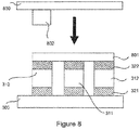
- the step of depositing the second capping layer may comprise depositing the second capping layer onto portions of a second substrate and aligning the second capping layer over at least the second portion of the plurality of OLEDs. This is illustrated in Figs. 8-9 , and will be described in more detail below.
- Embodiments may permit deposition using any known technique, such as using at least one of: photolithography, LITI, LIPS, stamping, or inkjet printing.
- the plurality of OLEDs may include a plurality of red OLEDs, a plurality of green OLEDs, and a plurality of blue OLEDs. This is typically the case for most displays (and light panels), as most colors can be replicated by using the combination of red, green, and blue light, including white light.
- the first and second portions of the plurality of OLEDs may each comprise OLEDs of particular colors, and in some embodiments there may not be any overlap.
- the first capping layer optimized for the light emissions in the blue spectrum (because the first capping layer may be optimized for only the blue OLEDs), while simultaneously optimizing the second capping layer for either the red or green OLEDs (or the second capping layer may have an optical thickness that is a compromise between the optimal optical thickness for each device).
- the second portion of the plurality of OLEDs comprises only a plurality of the red OLEDs or a plurality of the green OLEDs. The second capping layer may thereby be optimized for either of the light emissions of the green or red OLEDs.
- the inventors have recognized the benefits of depositing the third capping layer using these alternative techniques, such as using at least one of: laser induced thermal imaging (LITI) or laser induced pattern-wise sublimation (LIPS).
- LITI laser induced thermal imaging
- LIPS laser induced pattern-wise sublimation
- embodiments and features described herein may be combined and utilized with methods of fabricating devices, and the devices themselves, that comprise non-common capping layers that are deposited using such alternative deposition techniques ( i.e. not through the use of an FMM).
- the third capping layer may be deposited onto the second substrate using, for example, at least one of: photolithography, LITI, LIPS, stamping, or inkjet printing.
- the capping layer or layers are deposited on a second substrate allow for more options in the deposition process, typically a reduction in cost, and usually more error tolerance because the substrate does not comprise organic material, which may often be sensitive to such processes.
- the plurality of OLEDs include a plurality of red OLEDs, a plurality of green OLEDs, and a plurality of blue OLEDs
- the plurality of OLEDs also includes a third portion of OLEDs that is different from the first and second portions
- the method includes the step of depositing a third capping layer over at least the third portion of the plurality of OLEDs such that the third capping layer is optically coupled to at least the third portion of the plurality of OLEDs
- the first, second, and third portions of the plurality of OLEDs may each comprise OLEDs of various different colors.
- the optical thickness of the capping layer (or layers) that is optically coupled to the OLED be set to approximately the quarter wavelength of the OLED light emission. This may thereby reduce interference patterns and establish a maximum as to the amount of light emissions.
- the third capping layer when the third capping layer has an optical thickness that is optimized for the red OLEDs, the third capping layer has a thickness that is approximately within the range of 160 to 200 nm. As described above, when the first or the second capping layer is common to the third portion of the plurality of OLEDs, then the third capping layer may have an optical thickness such that the total optical thickness of the total capping layer that is optically coupled to the third portion of the plurality of OLEDs is optimized. As with the first and the second capping layers, the third capping layer may comprise any suitable material, such as Alq 3 . The third capping layer may be substantially transparent for light having a wavelength approximately equal to a wavelength of light that is emitted by each OLED that the third capping layer is optically coupled to. Moreover, in some embodiments, the third capping layer may have an index of refraction that is approximately in the range of 1 and 2.5 and preferably approximately within the range of 1.5 and 2.
- the first, second, and third capping layers may each be designed so as to optimize one of the emission colors simultaneously.
- the first capping layer has a thickness that is optimized for the plurality of blue OLEDs
- the second capping layer has a thickness that is optimized for the plurality of green OLEDs
- the third capping layer has a thickness that is optimized for the plurality of red OLEDs.
- the device as a whole may then operate at a higher efficiency because the emissions from each color OLED is also optimized.
- each capping layer by itself does not have to provide the entire optical thickness for optimizing an OLED, but may be designed to combine with other capping layers that are also optically coupled to an OLED.
- the first capping layer has an optical thickness that is approximately within the range of 90 to 130 nm
- the second capping layer has an optical thickness that is approximately within the range of 125 to 160 nm
- the third capping layer has an optical thickness that is approximately within the range of 160 to 200 nm. This may correspond to the optimal thicknesses for optimizing blue, green, and red OLEDs respectively.
- a first apparatus comprises a plurality of OLEDs, each OLED having a first electrode, a second electrode disposed over the first electrode; and an organic electroluminescent (EL) material disposed between the first and the second electrodes.
- the OLEDs may be disposed over a common substrate such that there light emissions may combined (as in a display).
- the first apparatus further includes a first capping layer that is disposed over the second electrode of at least a first portion of the plurality of OLEDs such that the first capping layer is optically coupled to at least the first portion of the plurality of OLEDs. In this manner, the first capping layer may increase the efficiency of the emissions of at least the first portion of the plurality of OLEDs, as was described above.
- the first apparatus also comprises a second capping layer.
- the second capping layer may be disposed over the second electrode of at least a second portion of the plurality of OLEDs such that the second capping layer is optically coupled to the second portion of the plurality of OLEDs but not the first portion of the plurality of OLEDs.
- the optical thickness of the total capping layer that is optically coupled to the second portion of the plurality of OLEDs may be different than that which is optically coupled to the first plurality of OLEDs. This may, in some embodiments, provide the ability to optimize more than a single color OLED in such devices.
- the second capping layer of the first apparatus is not disposed over at least one of the plurality of red OLEDs, green OLEDs, and blue OLEDs.
- the second capping layer is not disposed over the plurality of blue OLEDs. This may be the case when the first capping layer has an optical thickness that is optimized for the blue OLEDs such that an additional capping layer optically coupled to the blue OLEDs may not be necessary to achieve optimization.
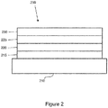
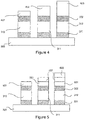
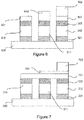
- Each of the exemplary devices shown in Figs. 3-9 comprise a plurality of OLEDs ( 310, 311 , and 312 ) that emit different colors (e.g . red, green, and blue respectively), each having a first electrode 321 and a second electrode 322, where the second electrode 322 are the top electrodes.
- Each of the OLEDs are disposed on a first substrate 300 .
- the first substrate may, for instance, comprise a backplane and/or TFT substrate. The remaining characteristics will be described in detail with respect to each figure.
- Fig. 4 shows a side view of an exemplary embodiment comprising a first capping layer 401, a second capping layer 402, and a third capping layer 403.
- the first capping layer 401 is not common to the plurality OLEDs 310, 311, and 312. Indeed, none of the capping layers are shown as optically coupled to any of the other capping layers, and none of the capping layers is common to a plurality of different color OLEDs.
- each of the capping layers 401, 402, and 403 may have an optical thickness that optimizes each of the OLEDs 310, 311, and 312 respectively.
- Fig. 6 shows a side view of an exemplary embodiment comprising a first capping layer 601 and second capping layer 602 .
- capping layer 601 is common to both OLED 310 and 312; and capping layer 602 is common to OLEDs 311 and 312.
- This embodiment illustrates that it is possible to have a device that comprises three different total capping layers while utilizing only two capping layers. That is, OLED 310 has a total capping layer comprising capping layer 601; OLED 311 has a total capping layer comprising capping layer 602; and OLED 312 has a total capping layer comprising capping layers 601 and 602.
- These embodiments have the advantage of only utilizing two deposition processes for depositing the capping layers, which may reduce time and costs of manufacturing.
- Fig. 7 shows a side view of an exemplary embodiment comprising a first capping layer 701, a second capping layer 702, and a third capping layer 703.
- Fig. 7 is almost identical to Fig. 5 in that capping layer 701 is common to all three OLEDs, capping layer 702 is common to OLEDs 311 and 312, and capping layer 503 is optically coupled to only OLED 312.
- Fig. 7 shows an embodiment whereby the capping layers comprise different physical thicknesses.
- this embodiment may have the advantage of providing increased adaptability so as to more readily optimize the emissions of each of the OLEDs.
- the red OLED (e.g. OLED 310 in Fig. 8 ) has the greatest loss of efficiency.
- providing capping layer 802 may offset or optimize OLED 310. It should be understood that some or all of the capping layers may be deposited on the second substrate 830, and in any combination, such as those discussed with reference to Figs. 3-7 .
- Figure 9 is similar to Fig. 8 in that the capping layers 902 and 903 are disposed on the second substrate 830, which may then be aligned and coupled to the first substrate 300. As shown, when the first 300 and second 830 substrate are coupled, capping layer 901 is common to all three OLEDs, capping layer 902 is common to OLEDs 311 and 312, and capping layer 903 is optically coupled to only OLED 312. Thus, the result is similar to the net effect provided by the capping layers in Figs. 5 and 7 .
- capping layers having the same or different optical properties may be provided so as to obtain different total optical thicknesses optically coupled to each of a plurality of different color OLED devices.
- the general principles remain the same as disclosed herein and are thereby contemplated as being within embodiments.
- Table 1 below shows the results of the simulations for power consumption for the exemplary 4-inch display described above, where the display has (1) the red, green, and blue pixels optimized separately with different capping layer optical thicknesses and (2) where the capping layer is optimized for the blue pixels only, but is common to red, green and blue pixels:
- the capping layer optically coupled to the red OLED comprised 100nm of Alq 3 and had an optical thickness of 170nm.
- the capping layer optically coupled to the green OLED comprised 80nm of Alq 3 and had an optical thickness of 138nm.
- the capping layer optically coupled to the blue OLED comprised 70nm of Alq 3 and had an optical thickness of 125nm.
- the light emission for this exemplary embodiment substantially increases for the red OLEDs (approximately 43.75% increase in luminance) and the green OLEDs (approximately 11.54% increase in luminance) when the capping layer that is optically coupled to each is optimized.
- the power consumption of the display decreased by 0.043 W (approximately 14.33%) as compared to the device having only a single optimized capping layer.
Landscapes
- Physics & Mathematics (AREA)
- Optics & Photonics (AREA)
- Chemical & Material Sciences (AREA)
- Inorganic Chemistry (AREA)
- Engineering & Computer Science (AREA)
- Manufacturing & Machinery (AREA)
- Electroluminescent Light Sources (AREA)
- Devices For Indicating Variable Information By Combining Individual Elements (AREA)
Applications Claiming Priority (2)
| Application Number | Priority Date | Filing Date | Title |
|---|---|---|---|
| US13/163,132 US8884316B2 (en) | 2011-06-17 | 2011-06-17 | Non-common capping layer on an organic device |
| EP12172237.5A EP2535960B1 (de) | 2011-06-17 | 2012-06-15 | Verfahren zum Herstellen einer nicht-gemeinsamen Deckschicht auf einer organischen Vorrichtung |
Related Parent Applications (2)
| Application Number | Title | Priority Date | Filing Date |
|---|---|---|---|
| EP12172237.5A Division EP2535960B1 (de) | 2011-06-17 | 2012-06-15 | Verfahren zum Herstellen einer nicht-gemeinsamen Deckschicht auf einer organischen Vorrichtung |
| EP12172237.5A Division-Into EP2535960B1 (de) | 2011-06-17 | 2012-06-15 | Verfahren zum Herstellen einer nicht-gemeinsamen Deckschicht auf einer organischen Vorrichtung |
Publications (1)
| Publication Number | Publication Date |
|---|---|
| EP3671882A1 true EP3671882A1 (de) | 2020-06-24 |
Family
ID=46651338
Family Applications (2)
| Application Number | Title | Priority Date | Filing Date |
|---|---|---|---|
| EP20155883.0A Pending EP3671882A1 (de) | 2011-06-17 | 2012-06-15 | Nicht-gemeinsame deckschicht auf einer organischen vorrichtung |
| EP12172237.5A Active EP2535960B1 (de) | 2011-06-17 | 2012-06-15 | Verfahren zum Herstellen einer nicht-gemeinsamen Deckschicht auf einer organischen Vorrichtung |
Family Applications After (1)
| Application Number | Title | Priority Date | Filing Date |
|---|---|---|---|
| EP12172237.5A Active EP2535960B1 (de) | 2011-06-17 | 2012-06-15 | Verfahren zum Herstellen einer nicht-gemeinsamen Deckschicht auf einer organischen Vorrichtung |
Country Status (5)
| Country | Link |
|---|---|
| US (4) | US8884316B2 (de) |
| EP (2) | EP3671882A1 (de) |
| JP (2) | JP6022225B2 (de) |
| KR (4) | KR101942571B1 (de) |
| CN (2) | CN103000824B (de) |
Cited By (1)
| Publication number | Priority date | Publication date | Assignee | Title |
|---|---|---|---|---|
| US12382782B2 (en) | 2018-05-18 | 2025-08-05 | Semiconductor Energy Laboratory Co., Ltd. | Estimation of cavity length of light-emitting device |
Families Citing this family (50)
| Publication number | Priority date | Publication date | Assignee | Title |
|---|---|---|---|---|
| US8940568B2 (en) | 2012-08-31 | 2015-01-27 | Universal Display Corporation | Patterning method for OLEDs |
| US9412947B2 (en) | 2012-09-14 | 2016-08-09 | Universal Display Corporation | OLED fabrication using laser transfer |
| KR102131965B1 (ko) * | 2013-11-19 | 2020-07-09 | 삼성디스플레이 주식회사 | 유기발광 디스플레이 장치 |
| KR102125881B1 (ko) * | 2014-04-29 | 2020-06-24 | 엘지디스플레이 주식회사 | 유기 발광 소자 |
| KR20150125889A (ko) | 2014-04-30 | 2015-11-10 | 삼성디스플레이 주식회사 | 유기발광 디스플레이 장치 및 그 제조방법 |
| US10356677B2 (en) * | 2014-05-19 | 2019-07-16 | Nokia Solutions And Networks Oy | Re-establishment procedure in dual connectivity networks |
| KR102304718B1 (ko) * | 2014-07-10 | 2021-09-27 | 삼성디스플레이 주식회사 | 유기 발광 소자 |
| KR102355605B1 (ko) * | 2014-11-20 | 2022-01-26 | 엘지디스플레이 주식회사 | 유기발광다이오드 표시장치 및 그 제조방법 |
| KR102424966B1 (ko) * | 2015-02-13 | 2022-07-26 | 삼성디스플레이 주식회사 | 유기발광 표시장치 |
| CN105098094B (zh) * | 2015-07-20 | 2017-11-17 | 上海和辉光电有限公司 | 显示面板及其oled元件 |
| KR102500272B1 (ko) | 2015-09-16 | 2023-02-16 | 삼성디스플레이 주식회사 | 화합물 및 이를 포함하는 유기 발광 소자 |
| KR102492730B1 (ko) | 2015-10-02 | 2023-01-27 | 삼성디스플레이 주식회사 | 유기 발광 표시 장치 |
| CN107017347A (zh) * | 2016-05-06 | 2017-08-04 | 广东聚华印刷显示技术有限公司 | 有机电致发光器件及其制备方法 |
| JP6817807B2 (ja) * | 2016-12-22 | 2021-01-20 | 株式会社ジャパンディスプレイ | 表示装置 |
| CN106601932B (zh) * | 2016-12-30 | 2020-10-23 | 上海天马有机发光显示技术有限公司 | 一种有机发光显示器件和装置 |
| CN106783935B (zh) * | 2017-01-16 | 2019-09-17 | 京东方科技集团股份有限公司 | 有机电致发光器件的封装结构及封装方法、显示装置 |
| CN106981502A (zh) * | 2017-04-27 | 2017-07-25 | 武汉华星光电技术有限公司 | 一种oled显示面板及其制作方法 |
| KR20190060908A (ko) * | 2017-11-24 | 2019-06-04 | 삼성디스플레이 주식회사 | 발광 소자 |
| US10892297B2 (en) | 2017-11-27 | 2021-01-12 | Seoul Viosys Co., Ltd. | Light emitting diode (LED) stack for a display |
| US11527519B2 (en) | 2017-11-27 | 2022-12-13 | Seoul Viosys Co., Ltd. | LED unit for display and display apparatus having the same |
| US12100696B2 (en) | 2017-11-27 | 2024-09-24 | Seoul Viosys Co., Ltd. | Light emitting diode for display and display apparatus having the same |
| US10892296B2 (en) | 2017-11-27 | 2021-01-12 | Seoul Viosys Co., Ltd. | Light emitting device having commonly connected LED sub-units |
| US11282981B2 (en) | 2017-11-27 | 2022-03-22 | Seoul Viosys Co., Ltd. | Passivation covered light emitting unit stack |
| CN107808934A (zh) | 2017-11-30 | 2018-03-16 | 武汉天马微电子有限公司 | 有机发光显示面板和显示装置 |
| US10748881B2 (en) | 2017-12-05 | 2020-08-18 | Seoul Viosys Co., Ltd. | Light emitting device with LED stack for display and display apparatus having the same |
| US10886327B2 (en) | 2017-12-14 | 2021-01-05 | Seoul Viosys Co., Ltd. | Light emitting stacked structure and display device having the same |
| US11552057B2 (en) | 2017-12-20 | 2023-01-10 | Seoul Viosys Co., Ltd. | LED unit for display and display apparatus having the same |
| US11522006B2 (en) | 2017-12-21 | 2022-12-06 | Seoul Viosys Co., Ltd. | Light emitting stacked structure and display device having the same |
| US11552061B2 (en) | 2017-12-22 | 2023-01-10 | Seoul Viosys Co., Ltd. | Light emitting device with LED stack for display and display apparatus having the same |
| US11114499B2 (en) | 2018-01-02 | 2021-09-07 | Seoul Viosys Co., Ltd. | Display device having light emitting stacked structure |
| US10784240B2 (en) | 2018-01-03 | 2020-09-22 | Seoul Viosys Co., Ltd. | Light emitting device with LED stack for display and display apparatus having the same |
| KR102597673B1 (ko) | 2018-05-16 | 2023-11-02 | 삼성디스플레이 주식회사 | 표시 장치 |
| US11217762B2 (en) * | 2018-11-30 | 2022-01-04 | Universal Display Corporation | Surface-plasmon-pumped light emitting devices |
| CN109686864A (zh) * | 2019-01-23 | 2019-04-26 | 武汉华星光电半导体显示技术有限公司 | 有机发光装置、显示装置 |
| KR102758040B1 (ko) | 2019-02-14 | 2025-01-23 | 삼성디스플레이 주식회사 | 유기 발광 소자 및 이를 포함한 발광 장치 |
| CN110277509B (zh) * | 2019-06-24 | 2022-09-02 | 昆山国显光电有限公司 | 一种显示面板和显示装置 |
| CN110444680A (zh) * | 2019-07-18 | 2019-11-12 | 武汉华星光电半导体显示技术有限公司 | 有机发光二极管显示面板及其制作方法和显示装置 |
| CN110649076B (zh) * | 2019-09-29 | 2022-04-05 | 上海天马微电子有限公司 | 有机发光显示面板和显示装置 |
| CN111129359A (zh) * | 2019-12-09 | 2020-05-08 | 武汉华星光电半导体显示技术有限公司 | 一种掩膜板组、oled面板及其制备方法 |
| KR20260036028A (ko) * | 2019-12-24 | 2026-03-13 | 오티아이 루미오닉스 인크. | 캡핑 층을 포함하는 발광 장치 및 그 제조방법 |
| KR102906653B1 (ko) * | 2020-06-02 | 2025-12-31 | 삼성전자주식회사 | 양자점 소자와 양자점 표시 장치 |
| CN111668282A (zh) * | 2020-07-03 | 2020-09-15 | 武汉华星光电半导体显示技术有限公司 | Oled显示面板及显示装置 |
| CN112490265B (zh) * | 2020-11-27 | 2022-08-02 | 电子科技大学 | 一种上转换低开启电压红外探测-发光器件及其制备方法 |
| CN112838177A (zh) * | 2021-02-26 | 2021-05-25 | 京东方科技集团股份有限公司 | Oled显示基板及其制作方法、显示装置 |
| CN113178467B (zh) * | 2021-04-14 | 2022-07-29 | 武汉华星光电半导体显示技术有限公司 | 显示面板及显示装置 |
| CN113193150B (zh) | 2021-04-28 | 2023-06-16 | 合肥京东方卓印科技有限公司 | 顶发光显示面板及显示装置 |
| CN115347030A (zh) * | 2022-08-25 | 2022-11-15 | 京东方科技集团股份有限公司 | 显示面板及显示装置 |
| CN115666161A (zh) * | 2022-10-31 | 2023-01-31 | 维信诺科技股份有限公司 | 显示面板及显示装置 |
| CN117479567A (zh) * | 2023-06-29 | 2024-01-30 | 武汉华星光电半导体显示技术有限公司 | 显示面板及显示装置 |
| KR102905842B1 (ko) | 2023-08-08 | 2025-12-31 | 주식회사 엘지유플러스 | 셋톱 박스의 상태 진단을 위한 전자 장치 및 그 동작 방법 |
Citations (23)
| Publication number | Priority date | Publication date | Assignee | Title |
|---|---|---|---|---|
| US4769292A (en) | 1987-03-02 | 1988-09-06 | Eastman Kodak Company | Electroluminescent device with modified thin film luminescent zone |
| US5247190A (en) | 1989-04-20 | 1993-09-21 | Cambridge Research And Innovation Limited | Electroluminescent devices |
| US5703436A (en) | 1994-12-13 | 1997-12-30 | The Trustees Of Princeton University | Transparent contacts for organic devices |
| US5707745A (en) | 1994-12-13 | 1998-01-13 | The Trustees Of Princeton University | Multicolor organic light emitting devices |
| US5834893A (en) | 1996-12-23 | 1998-11-10 | The Trustees Of Princeton University | High efficiency organic light emitting devices with light directing structures |
| US5844363A (en) | 1997-01-23 | 1998-12-01 | The Trustees Of Princeton Univ. | Vacuum deposited, non-polymeric flexible organic light emitting devices |
| US6013982A (en) | 1996-12-23 | 2000-01-11 | The Trustees Of Princeton University | Multicolor display devices |
| US6087196A (en) | 1998-01-30 | 2000-07-11 | The Trustees Of Princeton University | Fabrication of organic semiconductor devices using ink jet printing |
| US6091195A (en) | 1997-02-03 | 2000-07-18 | The Trustees Of Princeton University | Displays having mesa pixel configuration |
| US6097147A (en) | 1998-09-14 | 2000-08-01 | The Trustees Of Princeton University | Structure for high efficiency electroluminescent device |
| US6294398B1 (en) | 1999-11-23 | 2001-09-25 | The Trustees Of Princeton University | Method for patterning devices |
| US6303238B1 (en) | 1997-12-01 | 2001-10-16 | The Trustees Of Princeton University | OLEDs doped with phosphorescent compounds |
| US6337102B1 (en) | 1997-11-17 | 2002-01-08 | The Trustees Of Princeton University | Low pressure vapor phase deposition of organic thin films |
| US20030230980A1 (en) | 2002-06-18 | 2003-12-18 | Forrest Stephen R | Very low voltage, high efficiency phosphorescent oled in a p-i-n structure |
| US20040174116A1 (en) | 2001-08-20 | 2004-09-09 | Lu Min-Hao Michael | Transparent electrodes |
| US6895667B2 (en) | 2001-04-13 | 2005-05-24 | The Trustees Of Princeton University | Transfer of patterned metal by cold-welding |
| US20060138945A1 (en) * | 2004-12-28 | 2006-06-29 | Wolk Martin B | Electroluminescent devices and methods of making electroluminescent devices including an optical spacer |
| US20060208631A1 (en) * | 2005-03-16 | 2006-09-21 | Sun-Hwa Kim | Organic light emitting display device and method of fabricating the same |
| US7279704B2 (en) | 2004-05-18 | 2007-10-09 | The University Of Southern California | Complexes with tridentate ligands |
| US20080023724A1 (en) * | 2005-03-24 | 2008-01-31 | Kyocera Corporation | Light emitting element, light emitting device having the same and method for manufacturing the same |
| WO2008097046A1 (en) * | 2007-02-05 | 2008-08-14 | Lg Chem, Ltd. | Organic light-emitting device having improved light-emitting efficiency and method for fabricating the same |
| US20110084291A1 (en) * | 2009-10-09 | 2011-04-14 | Samsung Mobile Display Co., Ltd. | Organic light emitting diode display |
| US7964439B2 (en) | 2002-12-20 | 2011-06-21 | The Trustees Of Princeton University | Methods of fabricating devices by transfer of organic material |
Family Cites Families (122)
| Publication number | Priority date | Publication date | Assignee | Title |
|---|---|---|---|---|
| US5061569A (en) | 1990-07-26 | 1991-10-29 | Eastman Kodak Company | Electroluminescent device with organic electroluminescent medium |
| EP0650955B1 (de) | 1993-11-01 | 1998-08-19 | Hodogaya Chemical Co., Ltd. | Aminverbindung und sie enthaltende Elektrolumineszenzvorrichtung |
| US6939625B2 (en) | 1996-06-25 | 2005-09-06 | Nôrthwestern University | Organic light-emitting diodes and methods for assembly and enhanced charge injection |
| US5998085A (en) | 1996-07-23 | 1999-12-07 | 3M Innovative Properties | Process for preparing high resolution emissive arrays and corresponding articles |
| CN1242135A (zh) * | 1996-12-23 | 2000-01-19 | 普林斯顿大学理事会 | 具有反光结构的发光装置 |
| US6528187B1 (en) | 1998-09-08 | 2003-03-04 | Fuji Photo Film Co., Ltd. | Material for luminescence element and luminescence element using the same |
| US6830828B2 (en) | 1998-09-14 | 2004-12-14 | The Trustees Of Princeton University | Organometallic complexes as phosphorescent emitters in organic LEDs |
| JP4136185B2 (ja) * | 1999-05-12 | 2008-08-20 | パイオニア株式会社 | 有機エレクトロルミネッセンス多色ディスプレイ及びその製造方法 |
| US6458475B1 (en) | 1999-11-24 | 2002-10-01 | The Trustee Of Princeton University | Organic light emitting diode having a blue phosphorescent molecule as an emitter |
| KR100377321B1 (ko) | 1999-12-31 | 2003-03-26 | 주식회사 엘지화학 | 피-형 반도체 성질을 갖는 유기 화합물을 포함하는 전기소자 |
| US20020121638A1 (en) | 2000-06-30 | 2002-09-05 | Vladimir Grushin | Electroluminescent iridium compounds with fluorinated phenylpyridines, phenylpyrimidines, and phenylquinolines and devices made with such compounds |
| JP2002050860A (ja) | 2000-08-04 | 2002-02-15 | Toray Eng Co Ltd | 実装方法および実装装置 |
| EP1325671B1 (de) | 2000-08-11 | 2012-10-24 | The Trustees Of Princeton University | Organometallische verbdindungen und emissionsverschobene organische elektrolumineszens |
| US6579630B2 (en) | 2000-12-07 | 2003-06-17 | Canon Kabushiki Kaisha | Deuterated semiconducting organic compounds used for opto-electronic devices |
| JP3812730B2 (ja) | 2001-02-01 | 2006-08-23 | 富士写真フイルム株式会社 | 遷移金属錯体及び発光素子 |
| JP4307000B2 (ja) | 2001-03-08 | 2009-08-05 | キヤノン株式会社 | 金属配位化合物、電界発光素子及び表示装置 |
| JP4310077B2 (ja) | 2001-06-19 | 2009-08-05 | キヤノン株式会社 | 金属配位化合物及び有機発光素子 |
| CN100440568C (zh) | 2001-06-20 | 2008-12-03 | 昭和电工株式会社 | 发光材料和有机发光装置 |
| US7250226B2 (en) | 2001-08-31 | 2007-07-31 | Nippon Hoso Kyokai | Phosphorescent compound, a phosphorescent composition and an organic light-emitting device |
| US7431968B1 (en) | 2001-09-04 | 2008-10-07 | The Trustees Of Princeton University | Process and apparatus for organic vapor jet deposition |
| US6835469B2 (en) | 2001-10-17 | 2004-12-28 | The University Of Southern California | Phosphorescent compounds and devices comprising the same |
| US7166368B2 (en) | 2001-11-07 | 2007-01-23 | E. I. Du Pont De Nemours And Company | Electroluminescent platinum compounds and devices made with such compounds |
| US6863997B2 (en) | 2001-12-28 | 2005-03-08 | The Trustees Of Princeton University | White light emitting OLEDs from combined monomer and aggregate emission |
| KR100691543B1 (ko) | 2002-01-18 | 2007-03-09 | 주식회사 엘지화학 | 새로운 전자 수송용 물질 및 이를 이용한 유기 발광 소자 |
| US6878975B2 (en) | 2002-02-08 | 2005-04-12 | Agilent Technologies, Inc. | Polarization field enhanced tunnel structures |
| US7189989B2 (en) | 2002-08-22 | 2007-03-13 | Fuji Photo Film Co., Ltd. | Light emitting element |
| JP4313308B2 (ja) | 2002-08-27 | 2009-08-12 | 富士フイルム株式会社 | 有機金属錯体、有機el素子及び有機elディスプレイ |
| KR20050072424A (ko) * | 2002-10-01 | 2005-07-11 | 코닌클리케 필립스 일렉트로닉스 엔.브이. | 광 출력이 향상된 전기발광 디스플레이 |
| US6687266B1 (en) | 2002-11-08 | 2004-02-03 | Universal Display Corporation | Organic light emitting materials and devices |
| JP4365199B2 (ja) | 2002-12-27 | 2009-11-18 | 富士フイルム株式会社 | 有機電界発光素子 |
| JP4365196B2 (ja) | 2002-12-27 | 2009-11-18 | 富士フイルム株式会社 | 有機電界発光素子 |
| US7338722B2 (en) | 2003-03-24 | 2008-03-04 | The University Of Southern California | Phenyl and fluorenyl substituted phenyl-pyrazole complexes of Ir |
| US7090928B2 (en) | 2003-04-01 | 2006-08-15 | The University Of Southern California | Binuclear compounds |
| EP1618170A2 (de) | 2003-04-15 | 2006-01-25 | Covion Organic Semiconductors GmbH | Mischungen von organischen zur emission befähigten halbleitern und matrixmaterialien, deren verwendung und elektronikbauteile enthaltend diese mischungen |
| US7029765B2 (en) | 2003-04-22 | 2006-04-18 | Universal Display Corporation | Organic light emitting devices having reduced pixel shrinkage |
| JP4673744B2 (ja) | 2003-05-29 | 2011-04-20 | 新日鐵化学株式会社 | 有機電界発光素子 |
| JP2005011610A (ja) | 2003-06-18 | 2005-01-13 | Nippon Steel Chem Co Ltd | 有機電界発光素子 |
| US20050025993A1 (en) | 2003-07-25 | 2005-02-03 | Thompson Mark E. | Materials and structures for enhancing the performance of organic light emitting devices |
| TWI390006B (zh) | 2003-08-07 | 2013-03-21 | Nippon Steel Chemical Co | Organic EL materials with aluminum clamps |
| DE10338550A1 (de) | 2003-08-19 | 2005-03-31 | Basf Ag | Übergangsmetallkomplexe mit Carbenliganden als Emitter für organische Licht-emittierende Dioden (OLEDs) |
| US20060269780A1 (en) | 2003-09-25 | 2006-11-30 | Takayuki Fukumatsu | Organic electroluminescent device |
| JP4822687B2 (ja) | 2003-11-21 | 2011-11-24 | 富士フイルム株式会社 | 有機電界発光素子 |
| US7332232B2 (en) | 2004-02-03 | 2008-02-19 | Universal Display Corporation | OLEDs utilizing multidentate ligand systems |
| EP2918590A1 (de) | 2004-03-11 | 2015-09-16 | Mitsubishi Chemical Corporation | Zusammensetzung für eine ladungstransportfolie und ionenzusammensetzung, ladetransportfolie und organische elektrolumineszenzvorrichtung damit, und herstellungsverfahren der organischen elektrolumineszenzvorrichtung und herstellungsverfahren der ladungstransportfolie |
| TW200531592A (en) | 2004-03-15 | 2005-09-16 | Nippon Steel Chemical Co | Organic electroluminescent device |
| JP4869565B2 (ja) | 2004-04-23 | 2012-02-08 | 富士フイルム株式会社 | 有機電界発光素子 |
| US7445855B2 (en) | 2004-05-18 | 2008-11-04 | The University Of Southern California | Cationic metal-carbene complexes |
| US7393599B2 (en) | 2004-05-18 | 2008-07-01 | The University Of Southern California | Luminescent compounds with carbene ligands |
| US7534505B2 (en) | 2004-05-18 | 2009-05-19 | The University Of Southern California | Organometallic compounds for use in electroluminescent devices |
| US7491823B2 (en) | 2004-05-18 | 2009-02-17 | The University Of Southern California | Luminescent compounds with carbene ligands |
| US7154114B2 (en) | 2004-05-18 | 2006-12-26 | Universal Display Corporation | Cyclometallated iridium carbene complexes for use as hosts |
| WO2005123873A1 (ja) | 2004-06-17 | 2005-12-29 | Konica Minolta Holdings, Inc. | 有機エレクトロルミネッセンス素子材料、有機エレクトロルミネッセンス素子、表示装置及び照明装置 |
| BRPI0512641A (pt) | 2004-06-28 | 2008-03-25 | Ciba Sc Holding Ag | complexos metálicos eletroluminescentes com triazóis e benzotriazóis |
| US20060008670A1 (en) | 2004-07-06 | 2006-01-12 | Chun Lin | Organic light emitting materials and devices |
| CN1725521B (zh) | 2004-07-16 | 2010-10-27 | 国际商业机器公司 | 光电子器件及其制造方法 |
| EP2271183B1 (de) | 2004-07-23 | 2015-03-18 | Konica Minolta Holdings, Inc. | Organisches Elektrolumineszenzbauelement, Bildschirm und Beleuchtungseinheit |
| KR100623696B1 (ko) | 2004-08-30 | 2006-09-19 | 삼성에스디아이 주식회사 | 고효율 유기 전계 발광 소자 및 그의 제조방법 |
| DE102004057072A1 (de) | 2004-11-25 | 2006-06-01 | Basf Ag | Verwendung von Übergangsmetall-Carbenkomplexen in organischen Licht-emittierenden Dioden (OLEDs) |
| US8121679B2 (en) | 2004-12-29 | 2012-02-21 | Fruitman Clinton O | Transcutaneous electrical nerve stimulator with hot or cold thermal application |
| US8362463B2 (en) | 2004-12-30 | 2013-01-29 | E. I. Du Pont De Nemours And Company | Organometallic complexes |
| GB2437453B (en) | 2005-02-04 | 2011-05-04 | Konica Minolta Holdings Inc | Material for organic electroluminescence element, organic electroluminescence element, display device and lighting device |
| KR100803125B1 (ko) | 2005-03-08 | 2008-02-14 | 엘지전자 주식회사 | 적색 인광 화합물 및 이를 사용한 유기전계발광소자 |
| JP5125502B2 (ja) | 2005-03-16 | 2013-01-23 | コニカミノルタホールディングス株式会社 | 有機エレクトロルミネッセンス素子材料、有機エレクトロルミネッセンス素子 |
| JP5258166B2 (ja) * | 2005-03-24 | 2013-08-07 | エルジー ディスプレイ カンパニー リミテッド | 発光素子、その発光素子を備えた発光装置及びその製造方法 |
| JP4927423B2 (ja) * | 2005-03-24 | 2012-05-09 | エルジー ディスプレイ カンパニー リミテッド | 発光装置及びその製造方法 |
| DE102005014284A1 (de) | 2005-03-24 | 2006-09-28 | Basf Ag | Verwendung von Verbindungen, welche aromatische oder heteroaromatische über Carbonyl-Gruppen enthaltende Gruppen verbundene Ringe enthalten, als Matrixmaterialien in organischen Leuchtdioden |
| JPWO2006103874A1 (ja) | 2005-03-29 | 2008-09-04 | コニカミノルタホールディングス株式会社 | 有機エレクトロルミネッセンス素子材料、有機エレクトロルミネッセンス素子、表示装置及び照明装置 |
| US7401369B2 (en) | 2005-04-14 | 2008-07-22 | Nike, Inc. | Fluid-filled bladder for footwear and other applications |
| WO2006114966A1 (ja) | 2005-04-18 | 2006-11-02 | Konica Minolta Holdings, Inc. | 有機エレクトロルミネッセンス素子、表示装置及び照明装置 |
| JP4645822B2 (ja) * | 2005-04-19 | 2011-03-09 | ソニー株式会社 | 画像表示装置および物体の検出方法 |
| US7807275B2 (en) | 2005-04-21 | 2010-10-05 | Universal Display Corporation | Non-blocked phosphorescent OLEDs |
| US9051344B2 (en) | 2005-05-06 | 2015-06-09 | Universal Display Corporation | Stability OLED materials and devices |
| JP4533796B2 (ja) | 2005-05-06 | 2010-09-01 | 富士フイルム株式会社 | 有機電界発光素子 |
| WO2006130598A2 (en) | 2005-05-31 | 2006-12-07 | Universal Display Corporation | Triphenylene hosts in phosphorescent light emitting diodes |
| CN101193875B (zh) | 2005-06-07 | 2011-05-11 | 新日铁化学株式会社 | 有机金属络合物和使用了其的有机电致发光元件 |
| US7638072B2 (en) | 2005-06-27 | 2009-12-29 | E. I. Du Pont De Nemours And Company | Electrically conductive polymer compositions |
| WO2007004380A1 (ja) | 2005-07-01 | 2007-01-11 | Konica Minolta Holdings, Inc. | 有機エレクトロルミネッセンス素子材料、有機エレクトロルミネッセンス素子、表示装置及び照明装置 |
| WO2007028417A1 (en) | 2005-09-07 | 2007-03-15 | Technische Universität Braunschweig | Triplett emitter having condensed five-membered rings |
| JP4887731B2 (ja) | 2005-10-26 | 2012-02-29 | コニカミノルタホールディングス株式会社 | 有機エレクトロルミネッセンス素子、表示装置及び照明装置 |
| WO2007063754A1 (ja) | 2005-12-01 | 2007-06-07 | Nippon Steel Chemical Co., Ltd. | 有機電界発光素子用化合物及び有機電界発光素子 |
| JPWO2007063796A1 (ja) | 2005-12-01 | 2009-05-07 | 新日鐵化学株式会社 | 有機電界発光素子 |
| BRPI0707552B8 (pt) | 2006-02-10 | 2020-05-05 | Universal Display Corp | complexos metálicos de ligantes imidazo [1,2-f] fenantridina e diimizado [1,2-a:1', 2'-c] quinazolina ciclometalados e análogos isoeletrônicos e benzanulados dos mesmos e dispositivos oled que os englobam |
| JP4823730B2 (ja) | 2006-03-20 | 2011-11-24 | 新日鐵化学株式会社 | 発光層化合物及び有機電界発光素子 |
| WO2007125714A1 (ja) | 2006-04-26 | 2007-11-08 | Idemitsu Kosan Co., Ltd. | 芳香族アミン誘導体及びそれらを用いた有機エレクトロルミネッセンス素子 |
| KR101384046B1 (ko) | 2006-05-11 | 2014-04-09 | 이데미쓰 고산 가부시키가이샤 | 유기 전계발광 소자 |
| KR20090016684A (ko) | 2006-06-02 | 2009-02-17 | 이데미쓰 고산 가부시키가이샤 | 유기 전기발광 소자용 재료 및 그것을 이용한 유기 전기발광 소자 |
| KR20090040896A (ko) | 2006-08-23 | 2009-04-27 | 이데미쓰 고산 가부시키가이샤 | 방향족 아민 유도체 및 이들을 이용한 유기 전기발광 소자 |
| JP2008059791A (ja) * | 2006-08-29 | 2008-03-13 | Canon Inc | 有機el素子アレイ |
| JP5178088B2 (ja) * | 2006-09-07 | 2013-04-10 | キヤノン株式会社 | 有機発光装置 |
| JP5589251B2 (ja) | 2006-09-21 | 2014-09-17 | コニカミノルタ株式会社 | 有機エレクトロルミネッセンス素子材料 |
| US8062769B2 (en) | 2006-11-09 | 2011-11-22 | Nippon Steel Chemical Co., Ltd. | Indolocarbazole compound for use in organic electroluminescent device and organic electroluminescent device |
| JP5133259B2 (ja) | 2006-11-24 | 2013-01-30 | 出光興産株式会社 | 芳香族アミン誘導体及びそれを用いた有機エレクトロルミネッセンス素子 |
| US8119255B2 (en) | 2006-12-08 | 2012-02-21 | Universal Display Corporation | Cross-linkable iridium complexes and organic light-emitting devices using the same |
| US8778508B2 (en) | 2006-12-08 | 2014-07-15 | Universal Display Corporation | Light-emitting organometallic complexes |
| JP5546255B2 (ja) | 2007-02-23 | 2014-07-09 | ビーエーエスエフ ソシエタス・ヨーロピア | 電界発光性のベンゾトリアゾールとの金属錯体 |
| JP2008225179A (ja) * | 2007-03-14 | 2008-09-25 | Sony Corp | 表示装置、表示装置の駆動方法、および電子機器 |
| EP2150556B1 (de) | 2007-04-26 | 2011-01-12 | Basf Se | Silane enthaltend phenothiazin-s-oxid oder phenothiazin-s,s-dioxid-gruppen und deren verwendung in oleds |
| WO2008156879A1 (en) | 2007-06-20 | 2008-12-24 | Universal Display Corporation | Blue phosphorescent imidazophenanthridine materials |
| KR101539789B1 (ko) | 2007-06-22 | 2015-07-27 | 바스프 에스이 | 발광 cu(i) 착물 |
| KR101577465B1 (ko) | 2007-07-05 | 2015-12-14 | 바스프 에스이 | 카르벤 전이 금속 착체 이미터, 및 디실릴카르바졸, 디실릴디벤조푸란, 디실릴디벤조티오펜, 디실릴디벤조포스폴, 디실릴디벤조티오펜 s-옥사이드 및 디실릴디벤조티오펜 s,s-디옥사이드로부터 선택된 1종 이상의 화합물을 포함하는 유기 발광 다이오드 |
| US8779655B2 (en) | 2007-07-07 | 2014-07-15 | Idemitsu Kosan Co., Ltd. | Organic electroluminescence device and material for organic electroluminescence device |
| TW200909560A (en) | 2007-07-07 | 2009-03-01 | Idemitsu Kosan Co | Organic electroluminescence device and material for organic electroluminescence devcie |
| KR20100031723A (ko) | 2007-07-07 | 2010-03-24 | 이데미쓰 고산 가부시키가이샤 | 크리센 유도체 및 이를 이용한 유기 전계 발광 소자 |
| JP5295957B2 (ja) | 2007-07-07 | 2013-09-18 | 出光興産株式会社 | ナフタレン誘導体、有機el素子用材料及びそれを用いた有機el素子 |
| US20090045731A1 (en) | 2007-07-07 | 2009-02-19 | Idemitsu Kosan Co., Ltd. | Organic electroluminescence device and material for organic electroluminescence device |
| US8080658B2 (en) | 2007-07-10 | 2011-12-20 | Idemitsu Kosan Co., Ltd. | Material for organic electroluminescent element and organic electroluminescent element employing the same |
| WO2009008100A1 (ja) | 2007-07-10 | 2009-01-15 | Idemitsu Kosan Co., Ltd. | 有機エレクトロルミネッセンス素子用材料及びそれを用いた有機エレクトロルミネッセンス素子 |
| CN101688052A (zh) | 2007-07-27 | 2010-03-31 | E.I.内穆尔杜邦公司 | 包含无机纳米颗粒的导电聚合物的含水分散体 |
| EP3159333B1 (de) | 2007-08-08 | 2020-04-22 | Universal Display Corporation | Benzokondensierte thiophen- oder furan- verbindungen mit einer triphenylengruppe |
| JP2009040728A (ja) | 2007-08-09 | 2009-02-26 | Canon Inc | 有機金属錯体及びこれを用いた有機発光素子 |
| WO2009050290A1 (de) | 2007-10-17 | 2009-04-23 | Basf Se | Übergangsmetallkomplexe mit verbrückten carbenliganden und deren verwendung in oleds |
| US20090101870A1 (en) | 2007-10-22 | 2009-04-23 | E. I. Du Pont De Nemours And Company | Electron transport bi-layers and devices made with such bi-layers |
| US7914908B2 (en) | 2007-11-02 | 2011-03-29 | Global Oled Technology Llc | Organic electroluminescent device having an azatriphenylene derivative |
| DE102007053771A1 (de) | 2007-11-12 | 2009-05-14 | Merck Patent Gmbh | Organische Elektrolumineszenzvorrichtungen |
| CN101861291A (zh) | 2007-11-15 | 2010-10-13 | 出光兴产株式会社 | 苯并*衍生物及使用该衍生物的有机电致发光元件 |
| EP2221897A4 (de) | 2007-11-22 | 2012-08-08 | Idemitsu Kosan Co | Organisches el-element und ein organisches el-material enthaltende lösung |
| CN101868868A (zh) | 2007-11-22 | 2010-10-20 | 出光兴产株式会社 | 有机el元件 |
| JP2009164117A (ja) * | 2007-12-12 | 2009-07-23 | Fuji Electric Holdings Co Ltd | 有機elデバイスおよびその製造方法 |
| WO2009085344A2 (en) | 2007-12-28 | 2009-07-09 | Universal Display Corporation | Dibenzothiophene-containing materials in phosphorescent light emitting diodes |
| US8221905B2 (en) | 2007-12-28 | 2012-07-17 | Universal Display Corporation | Carbazole-containing materials in phosphorescent light emitting diodes |
| WO2009100991A1 (en) | 2008-02-12 | 2009-08-20 | Basf Se | Electroluminescent metal complexes with dibenzo[f,h]quinoxalines |
| KR101193186B1 (ko) * | 2010-02-01 | 2012-10-19 | 삼성디스플레이 주식회사 | 박막 증착 장치, 이를 이용한 유기 발광 디스플레이 장치의 제조방법 및 이에 따라 제조된 유기 발광 디스플레이 장치 |
-
2011
- 2011-06-17 US US13/163,132 patent/US8884316B2/en active Active
-
2012
- 2012-06-15 CN CN201210286949.3A patent/CN103000824B/zh active Active
- 2012-06-15 CN CN201610467166.3A patent/CN105957981B/zh active Active
- 2012-06-15 EP EP20155883.0A patent/EP3671882A1/de active Pending
- 2012-06-15 EP EP12172237.5A patent/EP2535960B1/de active Active
- 2012-06-18 JP JP2012136669A patent/JP6022225B2/ja active Active
- 2012-06-18 KR KR1020120065127A patent/KR101942571B1/ko active Active
-
2014
- 2014-10-06 US US14/507,104 patent/US10340313B2/en active Active
-
2016
- 2016-10-04 JP JP2016196228A patent/JP6479738B2/ja active Active
-
2019
- 2019-01-21 KR KR1020190007768A patent/KR102113946B1/ko active Active
- 2019-05-23 US US16/420,638 patent/US11751455B2/en active Active
-
2020
- 2020-01-23 KR KR1020200009061A patent/KR20200012007A/ko not_active Ceased
-
2021
- 2021-01-26 KR KR1020210011059A patent/KR20210013637A/ko not_active Ceased
-
2023
- 2023-08-04 US US18/365,273 patent/US20230380237A1/en active Pending
Patent Citations (24)
| Publication number | Priority date | Publication date | Assignee | Title |
|---|---|---|---|---|
| US4769292A (en) | 1987-03-02 | 1988-09-06 | Eastman Kodak Company | Electroluminescent device with modified thin film luminescent zone |
| US5247190A (en) | 1989-04-20 | 1993-09-21 | Cambridge Research And Innovation Limited | Electroluminescent devices |
| US5703436A (en) | 1994-12-13 | 1997-12-30 | The Trustees Of Princeton University | Transparent contacts for organic devices |
| US5707745A (en) | 1994-12-13 | 1998-01-13 | The Trustees Of Princeton University | Multicolor organic light emitting devices |
| US5834893A (en) | 1996-12-23 | 1998-11-10 | The Trustees Of Princeton University | High efficiency organic light emitting devices with light directing structures |
| US6013982A (en) | 1996-12-23 | 2000-01-11 | The Trustees Of Princeton University | Multicolor display devices |
| US5844363A (en) | 1997-01-23 | 1998-12-01 | The Trustees Of Princeton Univ. | Vacuum deposited, non-polymeric flexible organic light emitting devices |
| US6091195A (en) | 1997-02-03 | 2000-07-18 | The Trustees Of Princeton University | Displays having mesa pixel configuration |
| US6337102B1 (en) | 1997-11-17 | 2002-01-08 | The Trustees Of Princeton University | Low pressure vapor phase deposition of organic thin films |
| US6303238B1 (en) | 1997-12-01 | 2001-10-16 | The Trustees Of Princeton University | OLEDs doped with phosphorescent compounds |
| US6087196A (en) | 1998-01-30 | 2000-07-11 | The Trustees Of Princeton University | Fabrication of organic semiconductor devices using ink jet printing |
| US6097147A (en) | 1998-09-14 | 2000-08-01 | The Trustees Of Princeton University | Structure for high efficiency electroluminescent device |
| US6294398B1 (en) | 1999-11-23 | 2001-09-25 | The Trustees Of Princeton University | Method for patterning devices |
| US6468819B1 (en) | 1999-11-23 | 2002-10-22 | The Trustees Of Princeton University | Method for patterning organic thin film devices using a die |
| US6895667B2 (en) | 2001-04-13 | 2005-05-24 | The Trustees Of Princeton University | Transfer of patterned metal by cold-welding |
| US20040174116A1 (en) | 2001-08-20 | 2004-09-09 | Lu Min-Hao Michael | Transparent electrodes |
| US20030230980A1 (en) | 2002-06-18 | 2003-12-18 | Forrest Stephen R | Very low voltage, high efficiency phosphorescent oled in a p-i-n structure |
| US7964439B2 (en) | 2002-12-20 | 2011-06-21 | The Trustees Of Princeton University | Methods of fabricating devices by transfer of organic material |
| US7279704B2 (en) | 2004-05-18 | 2007-10-09 | The University Of Southern California | Complexes with tridentate ligands |
| US20060138945A1 (en) * | 2004-12-28 | 2006-06-29 | Wolk Martin B | Electroluminescent devices and methods of making electroluminescent devices including an optical spacer |
| US20060208631A1 (en) * | 2005-03-16 | 2006-09-21 | Sun-Hwa Kim | Organic light emitting display device and method of fabricating the same |
| US20080023724A1 (en) * | 2005-03-24 | 2008-01-31 | Kyocera Corporation | Light emitting element, light emitting device having the same and method for manufacturing the same |
| WO2008097046A1 (en) * | 2007-02-05 | 2008-08-14 | Lg Chem, Ltd. | Organic light-emitting device having improved light-emitting efficiency and method for fabricating the same |
| US20110084291A1 (en) * | 2009-10-09 | 2011-04-14 | Samsung Mobile Display Co., Ltd. | Organic light emitting diode display |
Non-Patent Citations (8)
| Title |
|---|
| BALDO ET AL.: "Highly Efficient Phosphorescent Emission from Organic Electroluminescent Devices", NATURE, vol. 395, 1998, pages 151 - 154, XP001002103, DOI: 10.1038/25954 |
| BALDO ET AL.: "Very high-efficiency green organic light-emitting devices based on electrophosphorescence", APPL. PHYS. LETT., vol. 75, no. 3, 1999, pages 4 - 6, XP012023409, DOI: 10.1063/1.124258 |
| H. RICLS. KARGT. BEIERLEINB. RUHSTALLERW. RIEB: "Phosphorescent Top-Emitting Organic Light-Emitting Devices With Improved Light Outcoupling", APPLIED PHYSICS LETTERS, vol. 82, no. 3, 20 January 2003 (2003-01-20) |
| H. RIEL ET AL., PHOSPHORESCENT TOP-EMITTING ORGANIC LIGHT-EMITTING DEVICES WITH IMPROVED LIGHT OUTCOUPLING,'' AND ''TUNING THE EMISSION CHARACTERISTICS OF TOP-EMITTING ORGANIC LIGHT-EMITTING DEVICES BY MEANS OF A DIELECTRIC CAPPING LAYER: AN EXPERIMENTAL AND THEORET |
| H. RIELS. KARGT. BEIERLEINB. RUHSTALLERW. RIEB: "Tuning the Emission Characteristics of Top-Emitting Organic Light-Emitting Devices By Means of a Dielectric Capping Layer: An Experimental and Theoretical Study", JOURNAL OF APPLIED PHYSICS, vol. 94, no. 8, 15 October 2003 (2003-10-15), XP012060416, DOI: 10.1063/1.1605256 |
| ST LEEBD CHINMH KIMTM KANGMW SONGJH LEEHD KIMHK CHUNGMB WOLKE BELLMAN: "A I novel patterning method for full-color organic light-emitting devices: laser induced thermal imaging (LITI", PROCEEDINGS OF THE SOCIETY FOR INFORMATION DISPLAY, DIGEST OF TECHNICAL PAPERS, vol. 35, no. 2, 2004, pages 1008 - 1011 |
| ST LEEJY LEEMH KIMMC SUHTM KANGYJ CHOIJY PARKJH KWONHK CHUNG: "New Patterning Method for Full-Color Polymer Light-Emitting Devices: Laser Induced Thermal i Imaging (LITI", PROCEEDINGS OF THE SOCIETYFOR INFORMATION DISPLAY, DIGEST OF TECHNICAL PAPERS, vol. 33, no. 2, 2002, pages 784 - 787 |
| T HIRANOK MATSUDAK KOHINATAK HANAWAT MATSUMIE MATSUDAT ISHIBASHIA YOSHIDAT SASAOKA: "Novel Laser Transfer Technology for Manufacturing Large-Sized Displays", PROCEEDINGS OF THE SOCIETY FOR INFORMATION DISPLAY, DIGEST OF TECHNICAL PAPERS, vol. 38, no. 2, 2007, pages 1592 - 1595, XP007013326 |
Cited By (1)
| Publication number | Priority date | Publication date | Assignee | Title |
|---|---|---|---|---|
| US12382782B2 (en) | 2018-05-18 | 2025-08-05 | Semiconductor Energy Laboratory Co., Ltd. | Estimation of cavity length of light-emitting device |
Also Published As
| Publication number | Publication date |
|---|---|
| CN103000824A (zh) | 2013-03-27 |
| JP2017004980A (ja) | 2017-01-05 |
| KR20200012007A (ko) | 2020-02-04 |
| JP6479738B2 (ja) | 2019-03-06 |
| KR20190010698A (ko) | 2019-01-30 |
| CN105957981B (zh) | 2018-06-05 |
| KR102113946B1 (ko) | 2020-05-22 |
| KR20210013637A (ko) | 2021-02-04 |
| US20120319145A1 (en) | 2012-12-20 |
| US20230380237A1 (en) | 2023-11-23 |
| US10340313B2 (en) | 2019-07-02 |
| US20190326363A1 (en) | 2019-10-24 |
| KR20120139610A (ko) | 2012-12-27 |
| JP6022225B2 (ja) | 2016-11-09 |
| KR101942571B1 (ko) | 2019-01-25 |
| US8884316B2 (en) | 2014-11-11 |
| JP2013008669A (ja) | 2013-01-10 |
| US20150021582A1 (en) | 2015-01-22 |
| EP2535960A1 (de) | 2012-12-19 |
| CN103000824B (zh) | 2016-08-03 |
| US11751455B2 (en) | 2023-09-05 |
| CN105957981A (zh) | 2016-09-21 |
| EP2535960B1 (de) | 2020-03-25 |
Similar Documents
| Publication | Publication Date | Title |
|---|---|---|
| US20230380237A1 (en) | Non-common capping layer on an organic device | |
| US8957579B2 (en) | Low image sticking OLED display | |
| US20240357858A1 (en) | Organic electroluminescent devices | |
| US9349955B2 (en) | Patterning method for OLEDs | |
| US8981640B2 (en) | Simplified patterned light panel | |
| CN115347032B (zh) | 混合型显示器 | |
| CN107665953B (zh) | 极高分辨率堆叠oled显示器和其制造方法 | |
| US11362311B2 (en) | Sub-electrode microlens array for organic light emitting devices | |
| US10811633B2 (en) | Method of increasing the flexibility of an AMOLDED display, a flexible display, and a product | |
| US20250089544A1 (en) | System and Method for Organic Electronic Device Patterning | |
| US20240052474A1 (en) | Organic vapor jet printing system | |
| US20220130946A1 (en) | OLED Display Design for Local Transparency |
Legal Events
| Date | Code | Title | Description |
|---|---|---|---|
| PUAI | Public reference made under article 153(3) epc to a published international application that has entered the european phase |
Free format text: ORIGINAL CODE: 0009012 |
|
| STAA | Information on the status of an ep patent application or granted ep patent |
Free format text: STATUS: THE APPLICATION HAS BEEN PUBLISHED |
|
| AC | Divisional application: reference to earlier application |
Ref document number: 2535960 Country of ref document: EP Kind code of ref document: P |
|
| AK | Designated contracting states |
Kind code of ref document: A1 Designated state(s): AL AT BE BG CH CY CZ DE DK EE ES FI FR GB GR HR HU IE IS IT LI LT LU LV MC MK MT NL NO PL PT RO RS SE SI SK SM TR |
|
| STAA | Information on the status of an ep patent application or granted ep patent |
Free format text: STATUS: REQUEST FOR EXAMINATION WAS MADE |
|
| 17P | Request for examination filed |
Effective date: 20201223 |
|
| RBV | Designated contracting states (corrected) |
Designated state(s): AL AT BE BG CH CY CZ DE DK EE ES FI FR GB GR HR HU IE IS IT LI LT LU LV MC MK MT NL NO PL PT RO RS SE SI SK SM TR |
|
| RAP3 | Party data changed (applicant data changed or rights of an application transferred) |
Owner name: UNIVERSAL DISPLAY CORPORATION |
|
| STAA | Information on the status of an ep patent application or granted ep patent |
Free format text: STATUS: EXAMINATION IS IN PROGRESS |
|
| 17Q | First examination report despatched |
Effective date: 20221021 |
|
| STAA | Information on the status of an ep patent application or granted ep patent |
Free format text: STATUS: THE APPLICATION IS DEEMED TO BE WITHDRAWN |