EP3672009A1 - Circuit de protection, dispositif électronique et procédé de fonctionnement d'un dispositif électronique - Google Patents
Circuit de protection, dispositif électronique et procédé de fonctionnement d'un dispositif électronique Download PDFInfo
- Publication number
- EP3672009A1 EP3672009A1 EP19217887.9A EP19217887A EP3672009A1 EP 3672009 A1 EP3672009 A1 EP 3672009A1 EP 19217887 A EP19217887 A EP 19217887A EP 3672009 A1 EP3672009 A1 EP 3672009A1
- Authority
- EP
- European Patent Office
- Prior art keywords
- circuit
- connection
- protective
- electronic device
- preferred embodiments
- Prior art date
- Legal status (The legal status is an assumption and is not a legal conclusion. Google has not performed a legal analysis and makes no representation as to the accuracy of the status listed.)
- Granted
Links
Images
Classifications
-
- H—ELECTRICITY
- H02—GENERATION; CONVERSION OR DISTRIBUTION OF ELECTRIC POWER
- H02H—EMERGENCY PROTECTIVE CIRCUIT ARRANGEMENTS
- H02H9/00—Emergency protective circuit arrangements for limiting excess current or voltage without disconnection
- H02H9/04—Emergency protective circuit arrangements for limiting excess current or voltage without disconnection responsive to excess voltage
-
- H—ELECTRICITY
- H04—ELECTRIC COMMUNICATION TECHNIQUE
- H04L—TRANSMISSION OF DIGITAL INFORMATION, e.g. TELEGRAPHIC COMMUNICATION
- H04L25/00—Baseband systems
- H04L25/02—Details ; arrangements for supplying electrical power along data transmission lines
- H04L25/0264—Arrangements for coupling to transmission lines
- H04L25/0266—Arrangements for providing Galvanic isolation, e.g. by means of magnetic or capacitive coupling
-
- H—ELECTRICITY
- H04—ELECTRIC COMMUNICATION TECHNIQUE
- H04B—TRANSMISSION
- H04B3/00—Line transmission systems
- H04B3/02—Details
-
- H—ELECTRICITY
- H04—ELECTRIC COMMUNICATION TECHNIQUE
- H04M—TELEPHONIC COMMUNICATION
- H04M1/00—Substation equipment, e.g. for use by subscribers
- H04M1/738—Interface circuits for coupling substations to external telephone lines
- H04M1/74—Interface circuits for coupling substations to external telephone lines with means for reducing interference; with means for reducing effects due to line faults
- H04M1/745—Protection devices or circuits for voltages surges on the line
-
- H—ELECTRICITY
- H04—ELECTRIC COMMUNICATION TECHNIQUE
- H04M—TELEPHONIC COMMUNICATION
- H04M2201/00—Electronic components, circuits, software, systems or apparatus used in telephone systems
- H04M2201/80—Electronic components, circuits, software, systems or apparatus used in telephone systems line protection circuits such as current or overvoltage protection circuits
Definitions
- the disclosure relates to a protective circuit for a connection of an electronic device, in particular a control unit, which can be used for data communication with a further unit.
- the disclosure further relates to an electronic device, in particular a control device, with at least one such protective circuit and a method for operating an electronic device.
- Preferred embodiments relate to a protective circuit for a connection of an electronic device, in particular a control unit, which can be used for data communication with a further unit, the protective circuit having a parallel circuit comprising a diode and a capacitor circuit having at least one capacitor, a first connection of the parallel circuit to the Connection of the electronic device is connectable, and wherein a second connection of the parallel connection can be connected to the further unit, in particular at least indirectly (eg via a signal line), and an anode of the diode is connected to the first connection of the parallel connection.
- This advantageously enables reliable protection of the connection of the electronic device without restricting a transmission bandwidth.
- static signal levels for data communication can advantageously also be transmitted from the electronic device to the further unit by means of the protective circuit.
- protection by the protection circuit can be scaled as desired with the granularity of one.
- a corresponding protective circuit can be provided for each connection of the electronic device to be protected, which provides comparable protection for each of the plurality of connections.
- the diode is a Schottky diode.
- a first resistor is connected between a second connection of the parallel connection and a first electrical reference potential.
- the second connection of the parallel connection and / or a signal line which may be connected to it e.g. leads to a corresponding connection of the further unit, advantageously be held in a predeterminable direct voltage reference to the first electrical reference potential.
- the first electrical reference potential corresponds, for example, to a ground potential.
- a second resistor is connected between the first connection of the parallel connection and a second electrical reference potential.
- the first connection of the parallel connection and / or, if necessary, to it connected signal line are advantageously kept in a predeterminable DC voltage reference to the second electrical reference potential.
- the second electrical reference potential corresponds, for example, to a supply voltage for the module to be protected, that is to say, for example, to a supply voltage of the electronic device to which the protective circuit is assigned.
- FIG. 1 For an electronic device having a plurality of connections for data communication with a further unit, the protection device having at least one protection circuit according to the embodiments, which is assigned to at least one of the plurality of connections.
- the at least one protective circuit and / or the at least one protective device is integrated in the electronic device. This results in a particularly small configuration.
- FIG. 1 For brevity, the figures in this way, the at least one connection of the electronic device can be protected by the protective circuit or protective device according to the embodiments.
- the electronic device sends at least one first signal, in particular a digital signal, to a further unit via the at least one protective circuit and / or the at least one protective device.
- the capacitor circuit of the protection circuit advantageously transmits a slope of the signal to be transmitted or, in general, alternating components of the signal to be transmitted to the sink which is to receive the signal, for example the further unit described above, which is also the case in other preferred embodiments to an electronic Device and / or a control device and / or a peripheral device or the like can act.
- the capacitor circuit of the protective circuit transiently charges or discharges the network assigned to the signal sink or the corresponding signal line, but blocks DC components.
- the diode of the protective circuit results in an effective, high-impedance block for direct voltage emanating from the signal sink or the further unit, as can occur, for example, in the event of an error in which the signal line between the electronic device or its protective circuit and the further unit is short-circuited to a larger voltage, for example a supply voltage.
- the diode of the protective circuit transmits DC components of the signal to be transmitted from the source, that is to say the electronic device or the control device, to the signal sink, that is to say, for example, the further unit.
- the electronic device receives at least a second signal, in particular a digital signal, via the at least one protective circuit and / or the at least one protective device from one or the further unit.
- the further unit represents the signal source and the electronic device (or a corresponding connection) the signal sink.
- the capacitor circuit transmits the Protection circuit advantageously a slope (or generally alternating components) of the source signal to be sent from the signal source (in the present case the further unit) to the sink, that is to say the electronic device to be protected.
- the capacitor circuit of the protective circuit transiently charges or discharges the network assigned to the signal sink or the corresponding signal line or the connection, but blocks DC voltage components.
- the diode of the protective circuit results in an effective, high-impedance block for a DC voltage emanating from the signal source or the further unit, as can occur, for example, in the event of an error in which the signal line between the electronic device or its protective circuit and the other Unit is short-circuited to a larger voltage, for example a supply voltage.
- the diode of the protective circuit transfers DC voltage components from the sink, that is to say the electronic device or the control device, to the signal source, that is to say, for example, the further unit (“low-resistance charging”).
- the at least one protective circuit and / or the at least one protective device protects the at least one connection from overvoltages. In further preferred embodiments, this can be done, for example, in the manner described by way of example above with reference to the case of the transmission or reception of signals respectively.
- the principle according to the embodiments can be used for all electronic devices, and is particularly advantageous also for control devices for one Lighting device, in particular for motor vehicles, applicable. Further features, possible applications and advantages of further preferred embodiments result from the following description and the figures of the drawing. All of the described and illustrated features, alone or in any combination, form the subject matter of the invention, regardless of the patent claims or their dependency, and regardless of their wording or representation in the description or in the drawing.
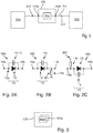
- FIG. 2 schematically shows a block diagram of a protection circuit 100 according to preferred embodiments.
- the protective circuit 100 is arranged, for example, in a target system which has an electronic device 200, in particular a control device, and a further unit 300 with which the device 200 can enter into data communication via a connection 210.
- the further unit 300 can be, for example, a peripheral device.
- Units 300 are each connected to the protective circuit 100, so that the aforementioned data communication between the units 200, 300 can take place via the protective circuit 100.
- the protective circuit 100 can have, for example, at least two connections 110a, 110b for contacting the connections 210, 310.
- the protective circuit 100 preferably has a preferred configuration 100a, for example in FIG Figure 2A a parallel circuit 110 comprising a diode 112 and a capacitor circuit 114 having at least one capacitor C1 is shown.
- the capacitor circuit 114 can also have, for example, a plurality of capacitors (not shown) which are connected, for example, electrically in parallel with one another. This creates further degrees of freedom with regard to the resulting total capacitance of the capacitor circuit 114 and / or a (temporal) operating behavior (for example with regard to the internal loss resistance, ESR, equivalent series resistance).
- ESR internal loss resistance
- a first connection 110a of the parallel connection can be connected to the connection 210 of the electronic device 200, a second connection 110b of the parallel connection 110 (at least indirectly, for example via a signal line 311) to the further unit 300 ( Fig. 1 ) is connectable, and wherein an anode 112a of the diode 112 is connected to the first terminal 110a of the parallel circuit 110.
- Reliable protection of the connection 210 ( Fig. 1 ) of the electronic device 200 without restricting a transmission bandwidth for data communication between the electronic device 200 and the further unit 300.
- static signal levels for this data communication can advantageously also be transmitted by means of the protective circuit 100.
- protection by the protection circuit 100 can be scaled as desired with the granularity of one.
- a corresponding protection circuit 100, 100a can be provided for each connection 210 of the electronic device 200 to be protected, which protection circuit realizes comparable protection for each of the connections 210.
- the diode 112 ( Figure 2A ) is a Schottky diode.
- Figure 2B shows an example of a circuit diagram according to further preferred embodiments 100b of the protective circuit.
- the protection circuit 100b after Figure 2B a first resistor 116a between the second terminal 110b of the parallel circuit 110 and a first electrical
- Reference potential BP1 switched.
- the second connection 110b of the parallel circuit 110 ( Fig. 1 ) and / or a signal line 311 possibly connected to it which leads, for example, to the connection 310 of the further unit 300, advantageously in a predeterminable direct voltage reference to the first electrical reference potential BP1 ( Figure 2B ) being held.
- the first electrical reference potential BP1 corresponds, for example, to a ground potential.
- Figure 2C shows an example of a circuit diagram according to further preferred embodiments 100c of the protective circuit.
- a second resistor 116b is connected between the first connection 110a of the parallel connection and a second electrical reference potential BP2.
- the first connection 110a of the parallel circuit 110 and / or a signal line which may be connected to it or the connection 210 can advantageously be kept in a predeterminable DC voltage reference to the second electrical reference potential BP2.
- the second corresponds to electrical Reference potential BP2, for example, a supply voltage for the module to be protected, for example a supply voltage of the electronic device 200, to which the protective circuit 100c is assigned.
- FIG. 3 schematically shows a block diagram of a protective device 1000 according to further preferred embodiments.
- the protective device 1000 has at least one, preferably several, protective circuits 100d, 100e according to the embodiments.
- Each of the two protective circuits 100d, 100e shown here as an example can, for example, have a configuration according to 2A or 2B or 2C have and for example be assigned to a corresponding connection of an electronic device 200 to be protected.
- the protective device 1000 advantageously enables efficient protection of one or more connections 210 ( Fig. 1 ) of an electronic device 200, and in further preferred embodiments can also be integrated into the electronic device 200, for example.
- one or more (individual) protective circuits according to the embodiments can also be integrated into the electronic device 200. Because of its compactness, it is also conceivable in further preferred embodiments to arrange the protective circuit directly on a (same) semiconductor substrate (not shown), such as the connection 210 of the device 200.
- FIG. 1 an electronic device 200 ( Fig. 1 ), in particular a control unit, with at least one connection 210 for data communication with a further unit 300, the device 200 having at least one protective circuit 100, 100a, 100b, 100c according to the embodiments and / or at least one protective device 1000 ( Fig. 3 ) according to the embodiments.
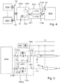
- FIG. 4 schematically shows a block diagram of a system according to further preferred embodiments.
- the system has a plurality of electronic devices, in particular control devices 200a, 200b, .., 200n, which are connected to one another by a bus system BS.
- the control device 200a has two connections 210a, 210b for data communication with a peripheral device 300a, wherein the two connections 210a, 210b are each electrically connected to corresponding connections (not shown) of the peripheral device 300a via a signal line 210a ', 210b'.
- Shown is a first electrical supply line BP1 ', which is connected to ground potential, for example.
- a second electrical supply line BP2 ' is shown, which is connected to an electrical potential which, based on the ground potential, corresponds to a supply voltage for the control unit 200a.
- the symbols B1, B2 symbolize an undesirable one Short circuit of at least one of the signal lines 210a ', 210b' to the second electrical supply line BP2 '.
- logic components or the entire control unit can be destroyed, for example, compare the symbol S1.
- the fault S1 due to the "overvoltage” can even spread via the bus system BS to the other control units 200b,..., 200n, cf. the symbols S2 in the bus system BS and the connections of the control devices 200b, 200n to the bus system BS, and disturb or damage them or the bus system BS.
- control unit 200a can be as shown schematically in FIG Figure 4 indicated according to further preferred embodiments, two protective circuits 100b, 100c (configuration, for example, accordingly Figures 2B, 2C ), with the protective circuit 100b being assigned, for example, to the first connection 210a and the protective circuit 100c, for example, to the second connection 210b of the control device 200a.
- the representation according to Figure 4 is a highly simplified, schematic representation, and the exact circuit topology regarding the integration of the respective protection circuit 100b, 100c in the relevant connections 210a, 210b, for example, according to Figure 1 results.
- the first port 110a ( Figure 2B ) according to the protection circuit 100b Figure 4 with the first connection 210a of the control device 200a according to Figure 4 connected
- the second connector 110b ( Figure 2B ) of the protection circuit 100b is connected to the signal line 210a ' Figure 4 connected (series connection from connection 210a, protection circuit 100b, signal line 210a ').
- control device 200a is designed to transmit data to the peripheral device 300a via the first connection 210a (and via the protection circuit 100b which is connected in series with respect to its connections 110a, 110b or its parallel connection 110), the relevant effect chain has the following elements in the order mentioned: first connection 210a, parallel circuit 110 of the protective circuit 100b in accordance with Figure 2B , Signal line 210a ', peripheral device 300a.
- control device 200a is designed to receive data via the second connection 210b (and via the protective circuit 100c) from the peripheral device 300a, the relevant device Function chain has the following elements in the order mentioned: peripheral device 300a, signal line 210b ', parallel circuit 110 of the protective circuit 100c in accordance with Figure 2C , second connection 210b.
- FIG 5 schematically shows a block diagram of a system with a protective device 1000a according to further preferred embodiments.
- the protective device 1000a has a protective circuit 100b (cf. Figure 2B ), which is assigned to a first connection 210a of a control device 200a 'and a protection circuit 100c (cf. Figure 2C ), which is assigned to a second connection 210b of the control device 200a '.
- the first connection 210a serves to send data from the control device 200a ′ to one Figure 5 Further unit not shown (for example peripheral device 300a analogous to Figure 4 ), and the second connection 210b serves to receive data from the further unit 300a.
- the second connection 110b of the protective circuit 100b (“transmitting branch”) is connected to a first driver circuit T1, which is derived from the non-differential output signal s_1, which characterizes the data to be sent from the control unit 200a 'to the further unit via the first connection 210a and the protective circuit 100b, generates a differential output signal ds_1.
- a first driver circuit T1 which is derived from the non-differential output signal s_1, which characterizes the data to be sent from the control unit 200a 'to the further unit via the first connection 210a and the protective circuit 100b, generates a differential output signal ds_1.
- An optional electrical energy supply device for the first driver circuit T1 is shown in FIG Figure 5 provided with the reference number 220.
- the second connection 110b of the protective circuit 100c (“receive branch”) is connected to the output of a second driver circuit T2, which consists of a differential receive signal ds_2, which signals the second driver circuit T2, the protective circuit 100c, from the further unit 300a via corresponding differential signal lines. characterizes the second connection 210b to the data to be sent to the control device 200a ', generates a non-differential receive signal s_2.
- the electrical energy supply of the second driver circuit T2 can also be accomplished by the energy supply device 220.
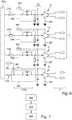
- FIG. 6 schematically shows a block diagram of a system with a protective device 1000b according to further preferred embodiments.
- the protective device 1000b in the present case has three protective circuits 100b (cf. Figure 2B ), which are each assigned to one of three transmission connections 210c, 210d, 210e of a control unit 200a ", and a protection circuit 100c ( Figure 2C ), which is assigned to a receive connection 210f of the control device 200a ".
- Output signals of the three protective circuits 100b are fed to a respective driver circuit T3, T4, T5, for generating differential signals which are sent to a further unit (not shown in FIG Fig. 6 shown, eg peripheral device 300a according to Fig. 4 ) be transmitted.
- the driver circuit T6 transforms a differential signal arriving via the signal lines L2 into a non-differential signal, which is fed to the connection 210f of the control unit 210a ′′ via the protection circuit 100c.
- One or more backup capacitors CS are optional provided that buffer the supply voltage BP3, for example for the driver circuits T3, T4, T5, T6.
- the signal lines L1, L2 provide, for example, a (eg TIA-644-2001-compliant) LVDS (low voltage differential signaling, signaling by means of differential low-voltage signals) interface, with three transmission signals via the connections 210c, 210d, 210e ("TX signals", based on the control unit 210a "), for example CLK, LATCH, DATA, can be implemented, and a receive signal (" RX response ") via the connection 210f.
- TX signals based on the control unit 210a "
- the driver circuits T3, T4, T5, T6 assigned to the control unit 200a "(possibly as well as driver circuits assigned to the further unit not shown) are supplied by a separate operating voltage BP3 of, for example, 3.3 volts (V), which at further preferred embodiments, for example, is comparable to the second electrical reference potential BP2, but is particularly preferably not electrically connected to the second electrical reference potential BP2.
- a separation of the separate operating voltage BP3 from the second electrical reference potential BP2 prevents the second electrical reference potential BP2 is also contaminated in the event of a fault in which the third operating voltage BP3 is contaminated.
- one or more of the signal lines L1, L2 are at an impermissibly high potential, e.g. corresponding to a voltage greater than the mentioned operating voltage BP3 of 3.3 volts, at least one of the driver circuits T3, T4, T5, T6 could be undefinedly damaged and it would be in conventional systems which do not have the protective circuits 110b, 110c , not to rule out that the corresponding overvoltage reaches one or more of the connections 210c, 210d, 210e, 210f.
- preferred embodiments by means of the protective circuits 110b, 110c of the protective device 1000b prevent a maximum permissible current (caused by the overvoltage) into the connections 210c,..., 210f from being exceeded and thus ensure the further uninfluenced operation of the control device 200a ".
- FIG. 7 schematically shows a simplified flow diagram of a method for operating an electronic device 200, 200a, 200a ', 200a "according to further preferred embodiments.
- step 400 at least one protection circuit 100, 100a, 100b, 100c according to the embodiments, for example for operating the electronic device Device.
- the at least one connection 210 ( Fig. 1 ) of the electronic device 200 are protected by the protective circuit or a protective device according to the embodiments.
- the electronic device 200 sends at least one first signal, in particular a digital signal, via the at least one protective circuit and / or the at least one protective device to a further unit 300, cf. optional step 402 Fig. 7 .
- the capacitor circuit 114 transmits, for example, the protection circuit 100b ( Figure 2B ) advantageously an edge steepness of the signal to be transmitted or generally alternating components of the signal to be transmitted to the sink which the signal is to receive, for example the further unit 300 described above.
- the capacitor circuit 114 charges or discharges ( Figure 2B ) the network assigned to the signal sink 300 or the corresponding signal line (cf.
- the protective circuit 100b has an effective, high-impedance block for the signal sink or the further unit 300 ( Fig. 1 ) outgoing DC voltage, as can occur, for example, in the event of a fault, in which the signal line between the electronic device or its protective circuit 100b and the further unit 300 is short-circuited to a larger voltage, for example a supply voltage.
- the diode 112 of the protection circuit 100b ( Figure 2B ) DC voltage components of the signal to be transmitted from the source, ie the electronic device or the Control unit to the signal sink.
- the electronic device provides at least one second signal, in particular a digital signal, via the at least one protective circuit 100c ( Fig. 5 ) and / or which receives at least one protective device from one or the further unit, cf. optional step 404 Fig. 7 .
- the further unit 300, 300a represents the signal source and the electronic device 200, 200a, 200a ', 200a "represents the signal sink.
- the capacitor circuit 114 transmits the protection circuit 100c ( Figure 2C ) advantageously a slope (or generally alternating components) of the source signal to be sent from the signal source (in the present case the further unit 300) to the sink, that is to say the electronic device 200 to be protected. Furthermore, the capacitor circuit 114 of the protective circuit 100c charges or discharges that Network assigned to the signal sink or the corresponding signal line or the connection 210a ( Fig. 5 ) transient, but blocks DC components.
- the diode 112 of the protective circuit 100c results in an effective, high-impedance block for DC voltage emanating from the signal source or the further unit 300, as can occur, for example, in the event of an error in which the signal line (see, for example, the signal line from the second Terminal 110b of protection circuit 100c to driver circuit T2 Fig. 5 ) between the electronic device or its protective circuit and the other Unit is short-circuited to a larger voltage, for example a supply voltage.
- the diode 112 of the protection circuit 100c ( Figure 2C ) DC voltage components from the sink, that is to say the electronic device or the control device to the signal source, that is to say, for example, the further unit (“low-resistance charging”).
- steps 402, 404 may be illustrative of FIG Fig. 7 described method can also be carried out in a different order and / or at least partially in parallel to one another (in particular in the case of a plurality of connections) and / or repeatedly, in particular periodically.
- the at least one protective circuit 100, 100a, 100b, 100c and / or the at least one protective device 1000, 1000a, 1000b protects the at least one connection 210 from overvoltages.
- this can, for example, refer to the example above with reference to 1 to 6 described manner.
- the principle according to the embodiments can be used for all electronic devices, in particular for digital signal transmissions, and is particularly advantageous also on control units for a lighting device, in particular for motor vehicles. applicable. Further advantages are the passive nature of the protective circuit, which does not require any energy (apart from possibly dissipated in the resistors 116a, 116b) (or its own power supply), the small installation space (easy to integrate), and the simple scalability.
- the protective circuit 100a can according to Figure 2A for example by pull-up resistors integrated in the control device 200 (not shown, for example integrated in individual ports corresponding to the connection 210), for example to the configuration 100c Figure 2C be supplemented.
Landscapes
- Engineering & Computer Science (AREA)
- Power Engineering (AREA)
- Computer Networks & Wireless Communication (AREA)
- Signal Processing (AREA)
- Emergency Protection Circuit Devices (AREA)
Applications Claiming Priority (1)
| Application Number | Priority Date | Filing Date | Title |
|---|---|---|---|
| DE102018133519.9A DE102018133519B3 (de) | 2018-12-21 | 2018-12-21 | Schutzschaltung, Schutzeinrichtung, Elektronische Vorrichtung und Verfahren zum Betreiben einer elektronischen Vorrichtung |
Publications (2)
| Publication Number | Publication Date |
|---|---|
| EP3672009A1 true EP3672009A1 (fr) | 2020-06-24 |
| EP3672009B1 EP3672009B1 (fr) | 2023-10-04 |
Family
ID=69104229
Family Applications (1)
| Application Number | Title | Priority Date | Filing Date |
|---|---|---|---|
| EP19217887.9A Active EP3672009B1 (fr) | 2018-12-21 | 2019-12-19 | Circuit de protection, dispositif électronique et procédé de fonctionnement d'un dispositif électronique |
Country Status (2)
| Country | Link |
|---|---|
| EP (1) | EP3672009B1 (fr) |
| DE (1) | DE102018133519B3 (fr) |
Citations (4)
| Publication number | Priority date | Publication date | Assignee | Title |
|---|---|---|---|---|
| US3860757A (en) * | 1973-06-25 | 1975-01-14 | Gte Automatic Electric Lab Inc | Lowpass circuit for physical party line applications in subscriber carrier telephone system |
| EP1120949A1 (fr) * | 2000-01-27 | 2001-08-01 | Mecelec Industries | Circuit et dispositif limiteur du courant et installation téléphonique incorporant un tel dispositif |
| DE20007619U1 (de) * | 2000-04-27 | 2001-08-30 | Krauss-Maffei Wegmann GmbH & Co.KG, 34127 Kassel | Einrichtung zur Reduktion der Antennenanzahl an einem Kampffahrzeug |
| US20140085951A1 (en) * | 2011-05-18 | 2014-03-27 | Renesas Electronics Corporation | Receiving circuit and signal receiving method |
Family Cites Families (2)
| Publication number | Priority date | Publication date | Assignee | Title |
|---|---|---|---|---|
| US9472948B2 (en) * | 2013-09-30 | 2016-10-18 | Infineon Technologies Ag | On chip reverse polarity protection compliant with ISO and ESD requirements |
| EP3155715B1 (fr) * | 2014-09-12 | 2018-03-14 | Philips Lighting Holding B.V. | Circuits d'alimentation électrique |
-
2018
- 2018-12-21 DE DE102018133519.9A patent/DE102018133519B3/de active Active
-
2019
- 2019-12-19 EP EP19217887.9A patent/EP3672009B1/fr active Active
Patent Citations (4)
| Publication number | Priority date | Publication date | Assignee | Title |
|---|---|---|---|---|
| US3860757A (en) * | 1973-06-25 | 1975-01-14 | Gte Automatic Electric Lab Inc | Lowpass circuit for physical party line applications in subscriber carrier telephone system |
| EP1120949A1 (fr) * | 2000-01-27 | 2001-08-01 | Mecelec Industries | Circuit et dispositif limiteur du courant et installation téléphonique incorporant un tel dispositif |
| DE20007619U1 (de) * | 2000-04-27 | 2001-08-30 | Krauss-Maffei Wegmann GmbH & Co.KG, 34127 Kassel | Einrichtung zur Reduktion der Antennenanzahl an einem Kampffahrzeug |
| US20140085951A1 (en) * | 2011-05-18 | 2014-03-27 | Renesas Electronics Corporation | Receiving circuit and signal receiving method |
Also Published As
| Publication number | Publication date |
|---|---|
| DE102018133519B3 (de) | 2020-03-05 |
| EP3672009B1 (fr) | 2023-10-04 |
Similar Documents
| Publication | Publication Date | Title |
|---|---|---|
| EP0858174A2 (fr) | Procédé et système pour transmèttre des données et de l'énergie | |
| EP3391602B1 (fr) | Agencement de circuits pour terminaison de ligne commutable d'un bus série | |
| DE2334698A1 (de) | Ueberspannungsschutzschaltung | |
| DE102013222786A1 (de) | Teilnehmerstation für ein Bussystem und Verfahren zur Reduzierung von leitungsgebundenen Emissionen in einem Bussystem | |
| EP1427086B2 (fr) | Appareil électrique et methode pour le faire fonctionner | |
| EP0090255A2 (fr) | Circuit de commande à trois états | |
| EP3066805B1 (fr) | Poste du réseau d'un système de bus et procédé pour la réduction d'émissions électromagnétiques dans un système de bus | |
| DE102017009352A1 (de) | Energiekoppler zum elektrischen Koppeln von elektrischen Bordnetzen und Verfahren zum elektrischen Koppeln von elektrischen Bordnetzen | |
| EP2980660A1 (fr) | Procédé et dispositif de surveillance et de commutation d'un circuit de charge | |
| EP2110950B1 (fr) | Circuit et procédé de transmission de tension de signal à l'intérieur d'un pilote d'un circuit semi-conducteur de puissance | |
| EP0364700B1 (fr) | Circuit de couplage à un bus | |
| EP3672009B1 (fr) | Circuit de protection, dispositif électronique et procédé de fonctionnement d'un dispositif électronique | |
| EP0643515B1 (fr) | Dispositif pour la transmission bidirectionnelle de données | |
| DE19813964A1 (de) | Bussystem mit einer Zentraleinheit eine Mehrzahl von Steuermodulen, insbesondere für Insassenschutzsysteme in Kraftfahrzeugen | |
| DE102009011225B3 (de) | Busankopplung | |
| WO2007073930A2 (fr) | Circuiterie de commutation pourvue d'un dispositif de protection contre les explosions | |
| DE69132259T2 (de) | Vorrichtung zur spannungseinstellung in einem multiplexübertragungssystem | |
| DE10200518B4 (de) | Spannungsbegrenzer für den Schnittstellenkreis eines Kommunikationsbusses | |
| WO2016062580A1 (fr) | Dispositif de commande d'un réseau électrique de bord multi-tensions | |
| DE102009004974A1 (de) | Busteilnehmer mit geregelter Sendestromquelle | |
| DE102016011257A1 (de) | Bus- und Kommunikationssystem zur gleichstromfreien Signalübertragung auf einem gemeinsamen Medium mit Terminierung | |
| DE102022207473B4 (de) | Transientenschutz | |
| DE102013113474B3 (de) | Verbindungseinrichtung, Verfahren zu deren Betrieb sowie Buskommunikationsvorrichtung | |
| DE10133441C2 (de) | Schaltungsanordnung zur Spannungssymmetrierung von Datenbussen | |
| EP3884626A1 (fr) | Dispositif d'affaiblissement de réflexions pour un bus d'un système de bus et procédé d'affaiblissement de réflexions lors d'une transmission de données dans un système de bus |
Legal Events
| Date | Code | Title | Description |
|---|---|---|---|
| PUAI | Public reference made under article 153(3) epc to a published international application that has entered the european phase |
Free format text: ORIGINAL CODE: 0009012 |
|
| STAA | Information on the status of an ep patent application or granted ep patent |
Free format text: STATUS: THE APPLICATION HAS BEEN PUBLISHED |
|
| AK | Designated contracting states |
Kind code of ref document: A1 Designated state(s): AL AT BE BG CH CY CZ DE DK EE ES FI FR GB GR HR HU IE IS IT LI LT LU LV MC MK MT NL NO PL PT RO RS SE SI SK SM TR |
|
| AX | Request for extension of the european patent |
Extension state: BA ME |
|
| STAA | Information on the status of an ep patent application or granted ep patent |
Free format text: STATUS: REQUEST FOR EXAMINATION WAS MADE |
|
| 17P | Request for examination filed |
Effective date: 20201215 |
|
| RBV | Designated contracting states (corrected) |
Designated state(s): AL AT BE BG CH CY CZ DE DK EE ES FI FR GB GR HR HU IE IS IT LI LT LU LV MC MK MT NL NO PL PT RO RS SE SI SK SM TR |
|
| RIN1 | Information on inventor provided before grant (corrected) |
Inventor name: WOLF, MANUEL Inventor name: LAUBENSTEIN, RUEDIGER Inventor name: HORBELT, MARKUS |
|
| GRAP | Despatch of communication of intention to grant a patent |
Free format text: ORIGINAL CODE: EPIDOSNIGR1 |
|
| STAA | Information on the status of an ep patent application or granted ep patent |
Free format text: STATUS: GRANT OF PATENT IS INTENDED |
|
| RIC1 | Information provided on ipc code assigned before grant |
Ipc: H04M 3/18 20060101ALN20230321BHEP Ipc: H04M 1/74 20060101ALN20230321BHEP Ipc: H04B 3/02 20060101ALN20230321BHEP Ipc: H04L 25/02 20060101ALI20230321BHEP Ipc: H02H 9/04 20060101AFI20230321BHEP |
|
| INTG | Intention to grant announced |
Effective date: 20230414 |
|
| GRAS | Grant fee paid |
Free format text: ORIGINAL CODE: EPIDOSNIGR3 |
|
| GRAA | (expected) grant |
Free format text: ORIGINAL CODE: 0009210 |
|
| STAA | Information on the status of an ep patent application or granted ep patent |
Free format text: STATUS: THE PATENT HAS BEEN GRANTED |
|
| AK | Designated contracting states |
Kind code of ref document: B1 Designated state(s): AL AT BE BG CH CY CZ DE DK EE ES FI FR GB GR HR HU IE IS IT LI LT LU LV MC MK MT NL NO PL PT RO RS SE SI SK SM TR |
|
| RAP3 | Party data changed (applicant data changed or rights of an application transferred) |
Owner name: MARELLI AUTOMOTIVE LIGHTING REUTLINGEN (GERMANY) GMBH |
|
| REG | Reference to a national code |
Ref country code: GB Ref legal event code: FG4D Free format text: NOT ENGLISH |
|
| REG | Reference to a national code |
Ref country code: CH Ref legal event code: EP |
|
| REG | Reference to a national code |
Ref country code: IE Ref legal event code: FG4D Free format text: LANGUAGE OF EP DOCUMENT: GERMAN |
|
| REG | Reference to a national code |
Ref country code: DE Ref legal event code: R096 Ref document number: 502019009549 Country of ref document: DE |
|
| REG | Reference to a national code |
Ref country code: LT Ref legal event code: MG9D |
|
| REG | Reference to a national code |
Ref country code: NL Ref legal event code: MP Effective date: 20231004 |
|
| PG25 | Lapsed in a contracting state [announced via postgrant information from national office to epo] |
Ref country code: NL Free format text: LAPSE BECAUSE OF FAILURE TO SUBMIT A TRANSLATION OF THE DESCRIPTION OR TO PAY THE FEE WITHIN THE PRESCRIBED TIME-LIMIT Effective date: 20231004 |
|
| PG25 | Lapsed in a contracting state [announced via postgrant information from national office to epo] |
Ref country code: GR Free format text: LAPSE BECAUSE OF FAILURE TO SUBMIT A TRANSLATION OF THE DESCRIPTION OR TO PAY THE FEE WITHIN THE PRESCRIBED TIME-LIMIT Effective date: 20240105 |
|
| PG25 | Lapsed in a contracting state [announced via postgrant information from national office to epo] |
Ref country code: IS Free format text: LAPSE BECAUSE OF FAILURE TO SUBMIT A TRANSLATION OF THE DESCRIPTION OR TO PAY THE FEE WITHIN THE PRESCRIBED TIME-LIMIT Effective date: 20240204 |
|
| PG25 | Lapsed in a contracting state [announced via postgrant information from national office to epo] |
Ref country code: LT Free format text: LAPSE BECAUSE OF FAILURE TO SUBMIT A TRANSLATION OF THE DESCRIPTION OR TO PAY THE FEE WITHIN THE PRESCRIBED TIME-LIMIT Effective date: 20231004 |
|
| PG25 | Lapsed in a contracting state [announced via postgrant information from national office to epo] |
Ref country code: ES Free format text: LAPSE BECAUSE OF FAILURE TO SUBMIT A TRANSLATION OF THE DESCRIPTION OR TO PAY THE FEE WITHIN THE PRESCRIBED TIME-LIMIT Effective date: 20231004 |
|
| PG25 | Lapsed in a contracting state [announced via postgrant information from national office to epo] |
Ref country code: LT Free format text: LAPSE BECAUSE OF FAILURE TO SUBMIT A TRANSLATION OF THE DESCRIPTION OR TO PAY THE FEE WITHIN THE PRESCRIBED TIME-LIMIT Effective date: 20231004 Ref country code: IS Free format text: LAPSE BECAUSE OF FAILURE TO SUBMIT A TRANSLATION OF THE DESCRIPTION OR TO PAY THE FEE WITHIN THE PRESCRIBED TIME-LIMIT Effective date: 20240204 Ref country code: GR Free format text: LAPSE BECAUSE OF FAILURE TO SUBMIT A TRANSLATION OF THE DESCRIPTION OR TO PAY THE FEE WITHIN THE PRESCRIBED TIME-LIMIT Effective date: 20240105 Ref country code: ES Free format text: LAPSE BECAUSE OF FAILURE TO SUBMIT A TRANSLATION OF THE DESCRIPTION OR TO PAY THE FEE WITHIN THE PRESCRIBED TIME-LIMIT Effective date: 20231004 Ref country code: BG Free format text: LAPSE BECAUSE OF FAILURE TO SUBMIT A TRANSLATION OF THE DESCRIPTION OR TO PAY THE FEE WITHIN THE PRESCRIBED TIME-LIMIT Effective date: 20240104 Ref country code: PT Free format text: LAPSE BECAUSE OF FAILURE TO SUBMIT A TRANSLATION OF THE DESCRIPTION OR TO PAY THE FEE WITHIN THE PRESCRIBED TIME-LIMIT Effective date: 20240205 |
|
| PG25 | Lapsed in a contracting state [announced via postgrant information from national office to epo] |
Ref country code: SE Free format text: LAPSE BECAUSE OF FAILURE TO SUBMIT A TRANSLATION OF THE DESCRIPTION OR TO PAY THE FEE WITHIN THE PRESCRIBED TIME-LIMIT Effective date: 20231004 Ref country code: RS Free format text: LAPSE BECAUSE OF FAILURE TO SUBMIT A TRANSLATION OF THE DESCRIPTION OR TO PAY THE FEE WITHIN THE PRESCRIBED TIME-LIMIT Effective date: 20231004 Ref country code: PL Free format text: LAPSE BECAUSE OF FAILURE TO SUBMIT A TRANSLATION OF THE DESCRIPTION OR TO PAY THE FEE WITHIN THE PRESCRIBED TIME-LIMIT Effective date: 20231004 Ref country code: NO Free format text: LAPSE BECAUSE OF FAILURE TO SUBMIT A TRANSLATION OF THE DESCRIPTION OR TO PAY THE FEE WITHIN THE PRESCRIBED TIME-LIMIT Effective date: 20240104 Ref country code: LV Free format text: LAPSE BECAUSE OF FAILURE TO SUBMIT A TRANSLATION OF THE DESCRIPTION OR TO PAY THE FEE WITHIN THE PRESCRIBED TIME-LIMIT Effective date: 20231004 Ref country code: HR Free format text: LAPSE BECAUSE OF FAILURE TO SUBMIT A TRANSLATION OF THE DESCRIPTION OR TO PAY THE FEE WITHIN THE PRESCRIBED TIME-LIMIT Effective date: 20231004 |
|
| REG | Reference to a national code |
Ref country code: DE Ref legal event code: R097 Ref document number: 502019009549 Country of ref document: DE |
|
| PG25 | Lapsed in a contracting state [announced via postgrant information from national office to epo] |
Ref country code: DK Free format text: LAPSE BECAUSE OF FAILURE TO SUBMIT A TRANSLATION OF THE DESCRIPTION OR TO PAY THE FEE WITHIN THE PRESCRIBED TIME-LIMIT Effective date: 20231004 |
|
| PG25 | Lapsed in a contracting state [announced via postgrant information from national office to epo] |
Ref country code: CZ Free format text: LAPSE BECAUSE OF FAILURE TO SUBMIT A TRANSLATION OF THE DESCRIPTION OR TO PAY THE FEE WITHIN THE PRESCRIBED TIME-LIMIT Effective date: 20231004 |
|
| PG25 | Lapsed in a contracting state [announced via postgrant information from national office to epo] |
Ref country code: SK Free format text: LAPSE BECAUSE OF FAILURE TO SUBMIT A TRANSLATION OF THE DESCRIPTION OR TO PAY THE FEE WITHIN THE PRESCRIBED TIME-LIMIT Effective date: 20231004 |
|
| PG25 | Lapsed in a contracting state [announced via postgrant information from national office to epo] |
Ref country code: SM Free format text: LAPSE BECAUSE OF FAILURE TO SUBMIT A TRANSLATION OF THE DESCRIPTION OR TO PAY THE FEE WITHIN THE PRESCRIBED TIME-LIMIT Effective date: 20231004 Ref country code: SK Free format text: LAPSE BECAUSE OF FAILURE TO SUBMIT A TRANSLATION OF THE DESCRIPTION OR TO PAY THE FEE WITHIN THE PRESCRIBED TIME-LIMIT Effective date: 20231004 Ref country code: RO Free format text: LAPSE BECAUSE OF FAILURE TO SUBMIT A TRANSLATION OF THE DESCRIPTION OR TO PAY THE FEE WITHIN THE PRESCRIBED TIME-LIMIT Effective date: 20231004 Ref country code: IT Free format text: LAPSE BECAUSE OF FAILURE TO SUBMIT A TRANSLATION OF THE DESCRIPTION OR TO PAY THE FEE WITHIN THE PRESCRIBED TIME-LIMIT Effective date: 20231004 Ref country code: EE Free format text: LAPSE BECAUSE OF FAILURE TO SUBMIT A TRANSLATION OF THE DESCRIPTION OR TO PAY THE FEE WITHIN THE PRESCRIBED TIME-LIMIT Effective date: 20231004 Ref country code: DK Free format text: LAPSE BECAUSE OF FAILURE TO SUBMIT A TRANSLATION OF THE DESCRIPTION OR TO PAY THE FEE WITHIN THE PRESCRIBED TIME-LIMIT Effective date: 20231004 Ref country code: CZ Free format text: LAPSE BECAUSE OF FAILURE TO SUBMIT A TRANSLATION OF THE DESCRIPTION OR TO PAY THE FEE WITHIN THE PRESCRIBED TIME-LIMIT Effective date: 20231004 |
|
| REG | Reference to a national code |
Ref country code: CH Ref legal event code: PL |
|
| PLBE | No opposition filed within time limit |
Free format text: ORIGINAL CODE: 0009261 |
|
| STAA | Information on the status of an ep patent application or granted ep patent |
Free format text: STATUS: NO OPPOSITION FILED WITHIN TIME LIMIT |
|
| PG25 | Lapsed in a contracting state [announced via postgrant information from national office to epo] |
Ref country code: LU Free format text: LAPSE BECAUSE OF NON-PAYMENT OF DUE FEES Effective date: 20231219 |
|
| PG25 | Lapsed in a contracting state [announced via postgrant information from national office to epo] |
Ref country code: MC Free format text: LAPSE BECAUSE OF FAILURE TO SUBMIT A TRANSLATION OF THE DESCRIPTION OR TO PAY THE FEE WITHIN THE PRESCRIBED TIME-LIMIT Effective date: 20231004 |
|
| REG | Reference to a national code |
Ref country code: BE Ref legal event code: MM Effective date: 20231231 |
|
| PG25 | Lapsed in a contracting state [announced via postgrant information from national office to epo] |
Ref country code: MC Free format text: LAPSE BECAUSE OF FAILURE TO SUBMIT A TRANSLATION OF THE DESCRIPTION OR TO PAY THE FEE WITHIN THE PRESCRIBED TIME-LIMIT Effective date: 20231004 Ref country code: LU Free format text: LAPSE BECAUSE OF NON-PAYMENT OF DUE FEES Effective date: 20231219 |
|
| 26N | No opposition filed |
Effective date: 20240705 |
|
| GBPC | Gb: european patent ceased through non-payment of renewal fee |
Effective date: 20240104 |
|
| REG | Reference to a national code |
Ref country code: IE Ref legal event code: MM4A |
|
| PG25 | Lapsed in a contracting state [announced via postgrant information from national office to epo] |
Ref country code: IE Free format text: LAPSE BECAUSE OF NON-PAYMENT OF DUE FEES Effective date: 20231219 |
|
| PG25 | Lapsed in a contracting state [announced via postgrant information from national office to epo] |
Ref country code: GB Free format text: LAPSE BECAUSE OF NON-PAYMENT OF DUE FEES Effective date: 20240104 |
|
| PG25 | Lapsed in a contracting state [announced via postgrant information from national office to epo] |
Ref country code: BE Free format text: LAPSE BECAUSE OF NON-PAYMENT OF DUE FEES Effective date: 20231231 |
|
| PG25 | Lapsed in a contracting state [announced via postgrant information from national office to epo] |
Ref country code: FR Free format text: LAPSE BECAUSE OF NON-PAYMENT OF DUE FEES Effective date: 20231231 |
|
| PG25 | Lapsed in a contracting state [announced via postgrant information from national office to epo] |
Ref country code: CH Free format text: LAPSE BECAUSE OF NON-PAYMENT OF DUE FEES Effective date: 20231231 |
|
| PG25 | Lapsed in a contracting state [announced via postgrant information from national office to epo] |
Ref country code: SI Free format text: LAPSE BECAUSE OF FAILURE TO SUBMIT A TRANSLATION OF THE DESCRIPTION OR TO PAY THE FEE WITHIN THE PRESCRIBED TIME-LIMIT Effective date: 20231004 |
|
| PG25 | Lapsed in a contracting state [announced via postgrant information from national office to epo] |
Ref country code: SI Free format text: LAPSE BECAUSE OF FAILURE TO SUBMIT A TRANSLATION OF THE DESCRIPTION OR TO PAY THE FEE WITHIN THE PRESCRIBED TIME-LIMIT Effective date: 20231004 Ref country code: IE Free format text: LAPSE BECAUSE OF NON-PAYMENT OF DUE FEES Effective date: 20231219 Ref country code: GB Free format text: LAPSE BECAUSE OF NON-PAYMENT OF DUE FEES Effective date: 20240104 Ref country code: FR Free format text: LAPSE BECAUSE OF NON-PAYMENT OF DUE FEES Effective date: 20231231 Ref country code: CH Free format text: LAPSE BECAUSE OF NON-PAYMENT OF DUE FEES Effective date: 20231231 Ref country code: BE Free format text: LAPSE BECAUSE OF NON-PAYMENT OF DUE FEES Effective date: 20231231 |
|
| PG25 | Lapsed in a contracting state [announced via postgrant information from national office to epo] |
Ref country code: FI Free format text: LAPSE BECAUSE OF FAILURE TO SUBMIT A TRANSLATION OF THE DESCRIPTION OR TO PAY THE FEE WITHIN THE PRESCRIBED TIME-LIMIT Effective date: 20231004 |
|
| PG25 | Lapsed in a contracting state [announced via postgrant information from national office to epo] |
Ref country code: CY Free format text: LAPSE BECAUSE OF FAILURE TO SUBMIT A TRANSLATION OF THE DESCRIPTION OR TO PAY THE FEE WITHIN THE PRESCRIBED TIME-LIMIT; INVALID AB INITIO Effective date: 20191219 |
|
| PG25 | Lapsed in a contracting state [announced via postgrant information from national office to epo] |
Ref country code: HU Free format text: LAPSE BECAUSE OF FAILURE TO SUBMIT A TRANSLATION OF THE DESCRIPTION OR TO PAY THE FEE WITHIN THE PRESCRIBED TIME-LIMIT; INVALID AB INITIO Effective date: 20191219 |
|
| PG25 | Lapsed in a contracting state [announced via postgrant information from national office to epo] |
Ref country code: TR Free format text: LAPSE BECAUSE OF FAILURE TO SUBMIT A TRANSLATION OF THE DESCRIPTION OR TO PAY THE FEE WITHIN THE PRESCRIBED TIME-LIMIT Effective date: 20231004 |
|
| REG | Reference to a national code |
Ref country code: AT Ref legal event code: MM01 Ref document number: 1618748 Country of ref document: AT Kind code of ref document: T Effective date: 20241219 |
|
| PG25 | Lapsed in a contracting state [announced via postgrant information from national office to epo] |
Ref country code: AT Free format text: LAPSE BECAUSE OF NON-PAYMENT OF DUE FEES Effective date: 20241219 |
|
| PGFP | Annual fee paid to national office [announced via postgrant information from national office to epo] |
Ref country code: AT Payment date: 20260410 Year of fee payment: 5 |
|
| PGFP | Annual fee paid to national office [announced via postgrant information from national office to epo] |
Ref country code: DE Payment date: 20260624 Year of fee payment: 7 |