EP3672365B1 - Procédé permettant d'effectuer une opération de décongélation à l'aide d'un appareil de décongélation - Google Patents
Procédé permettant d'effectuer une opération de décongélation à l'aide d'un appareil de décongélation Download PDFInfo
- Publication number
- EP3672365B1 EP3672365B1 EP19215531.5A EP19215531A EP3672365B1 EP 3672365 B1 EP3672365 B1 EP 3672365B1 EP 19215531 A EP19215531 A EP 19215531A EP 3672365 B1 EP3672365 B1 EP 3672365B1
- Authority
- EP
- European Patent Office
- Prior art keywords
- radio frequency
- variable
- defrosting
- network
- frequency signal
- Prior art date
- Legal status (The legal status is an assumption and is not a legal conclusion. Google has not performed a legal analysis and makes no representation as to the accuracy of the status listed.)
- Active
Links
Images








Classifications
-
- H—ELECTRICITY
- H05—ELECTRIC TECHNIQUES NOT OTHERWISE PROVIDED FOR
- H05B—ELECTRIC HEATING; ELECTRIC LIGHT SOURCES NOT OTHERWISE PROVIDED FOR; CIRCUIT ARRANGEMENTS FOR ELECTRIC LIGHT SOURCES, IN GENERAL
- H05B6/00—Heating by electric, magnetic or electromagnetic fields
- H05B6/46—Dielectric heating
- H05B6/48—Circuits
- H05B6/50—Circuits for monitoring or control
-
- H—ELECTRICITY
- H05—ELECTRIC TECHNIQUES NOT OTHERWISE PROVIDED FOR
- H05B—ELECTRIC HEATING; ELECTRIC LIGHT SOURCES NOT OTHERWISE PROVIDED FOR; CIRCUIT ARRANGEMENTS FOR ELECTRIC LIGHT SOURCES, IN GENERAL
- H05B6/00—Heating by electric, magnetic or electromagnetic fields
- H05B6/64—Heating using microwaves
- H05B6/6402—Aspects relating to the microwave cavity
-
- A—HUMAN NECESSITIES
- A23—FOODS OR FOODSTUFFS; TREATMENT THEREOF, NOT COVERED BY OTHER CLASSES
- A23B—PRESERVATION OF FOODS, FOODSTUFFS OR NON-ALCOHOLIC BEVERAGES; CHEMICAL RIPENING OF FRUIT OR VEGETABLES
- A23B2/00—Preservation of foods or foodstuffs, in general
- A23B2/80—Freezing; Subsequent thawing; Cooling
- A23B2/82—Thawing subsequent to freezing
-
- F—MECHANICAL ENGINEERING; LIGHTING; HEATING; WEAPONS; BLASTING
- F25—REFRIGERATION OR COOLING; COMBINED HEATING AND REFRIGERATION SYSTEMS; HEAT PUMP SYSTEMS; MANUFACTURE OR STORAGE OF ICE; LIQUEFACTION SOLIDIFICATION OF GASES
- F25D—REFRIGERATORS; COLD ROOMS; ICE-BOXES; COOLING OR FREEZING APPARATUS NOT OTHERWISE PROVIDED FOR
- F25D23/00—General constructional features
- F25D23/12—Arrangements of compartments additional to cooling compartments; Combinations of refrigerators with other equipment, e.g. stove
-
- G—PHYSICS
- G01—MEASURING; TESTING
- G01R—MEASURING ELECTRIC VARIABLES; MEASURING MAGNETIC VARIABLES
- G01R21/00—Arrangements for measuring electric power or power factor
- G01R21/006—Measuring power factor
-
- H—ELECTRICITY
- H05—ELECTRIC TECHNIQUES NOT OTHERWISE PROVIDED FOR
- H05B—ELECTRIC HEATING; ELECTRIC LIGHT SOURCES NOT OTHERWISE PROVIDED FOR; CIRCUIT ARRANGEMENTS FOR ELECTRIC LIGHT SOURCES, IN GENERAL
- H05B6/00—Heating by electric, magnetic or electromagnetic fields
- H05B6/64—Heating using microwaves
- H05B6/6435—Aspects relating to the user interface of the microwave heating apparatus
-
- H—ELECTRICITY
- H05—ELECTRIC TECHNIQUES NOT OTHERWISE PROVIDED FOR
- H05B—ELECTRIC HEATING; ELECTRIC LIGHT SOURCES NOT OTHERWISE PROVIDED FOR; CIRCUIT ARRANGEMENTS FOR ELECTRIC LIGHT SOURCES, IN GENERAL
- H05B6/00—Heating by electric, magnetic or electromagnetic fields
- H05B6/64—Heating using microwaves
- H05B6/6447—Method of operation or details of the microwave heating apparatus related to the use of detectors or sensors
- H05B6/645—Method of operation or details of the microwave heating apparatus related to the use of detectors or sensors using temperature sensors
-
- H—ELECTRICITY
- H05—ELECTRIC TECHNIQUES NOT OTHERWISE PROVIDED FOR
- H05B—ELECTRIC HEATING; ELECTRIC LIGHT SOURCES NOT OTHERWISE PROVIDED FOR; CIRCUIT ARRANGEMENTS FOR ELECTRIC LIGHT SOURCES, IN GENERAL
- H05B6/00—Heating by electric, magnetic or electromagnetic fields
- H05B6/64—Heating using microwaves
- H05B6/6447—Method of operation or details of the microwave heating apparatus related to the use of detectors or sensors
- H05B6/645—Method of operation or details of the microwave heating apparatus related to the use of detectors or sensors using temperature sensors
- H05B6/6455—Method of operation or details of the microwave heating apparatus related to the use of detectors or sensors using temperature sensors the sensors being infrared detectors
-
- H—ELECTRICITY
- H05—ELECTRIC TECHNIQUES NOT OTHERWISE PROVIDED FOR
- H05B—ELECTRIC HEATING; ELECTRIC LIGHT SOURCES NOT OTHERWISE PROVIDED FOR; CIRCUIT ARRANGEMENTS FOR ELECTRIC LIGHT SOURCES, IN GENERAL
- H05B6/00—Heating by electric, magnetic or electromagnetic fields
- H05B6/64—Heating using microwaves
- H05B6/6447—Method of operation or details of the microwave heating apparatus related to the use of detectors or sensors
- H05B6/6467—Method of operation or details of the microwave heating apparatus related to the use of detectors or sensors using detectors with R.F. transmitters
-
- H—ELECTRICITY
- H05—ELECTRIC TECHNIQUES NOT OTHERWISE PROVIDED FOR
- H05B—ELECTRIC HEATING; ELECTRIC LIGHT SOURCES NOT OTHERWISE PROVIDED FOR; CIRCUIT ARRANGEMENTS FOR ELECTRIC LIGHT SOURCES, IN GENERAL
- H05B6/00—Heating by electric, magnetic or electromagnetic fields
- H05B6/64—Heating using microwaves
- H05B6/66—Circuits
- H05B6/68—Circuits for monitoring or control
- H05B6/686—Circuits comprising a signal generator and power amplifier, e.g. using solid state oscillators
-
- H—ELECTRICITY
- H05—ELECTRIC TECHNIQUES NOT OTHERWISE PROVIDED FOR
- H05B—ELECTRIC HEATING; ELECTRIC LIGHT SOURCES NOT OTHERWISE PROVIDED FOR; CIRCUIT ARRANGEMENTS FOR ELECTRIC LIGHT SOURCES, IN GENERAL
- H05B6/00—Heating by electric, magnetic or electromagnetic fields
- H05B6/64—Heating using microwaves
- H05B6/66—Circuits
- H05B6/68—Circuits for monitoring or control
- H05B6/687—Circuits for monitoring or control for cooking
-
- H—ELECTRICITY
- H05—ELECTRIC TECHNIQUES NOT OTHERWISE PROVIDED FOR
- H05B—ELECTRIC HEATING; ELECTRIC LIGHT SOURCES NOT OTHERWISE PROVIDED FOR; CIRCUIT ARRANGEMENTS FOR ELECTRIC LIGHT SOURCES, IN GENERAL
- H05B6/00—Heating by electric, magnetic or electromagnetic fields
- H05B6/64—Heating using microwaves
- H05B6/66—Circuits
- H05B6/68—Circuits for monitoring or control
- H05B6/688—Circuits for monitoring or control for thawing
-
- H—ELECTRICITY
- H05—ELECTRIC TECHNIQUES NOT OTHERWISE PROVIDED FOR
- H05B—ELECTRIC HEATING; ELECTRIC LIGHT SOURCES NOT OTHERWISE PROVIDED FOR; CIRCUIT ARRANGEMENTS FOR ELECTRIC LIGHT SOURCES, IN GENERAL
- H05B6/00—Heating by electric, magnetic or electromagnetic fields
- H05B6/64—Heating using microwaves
- H05B6/70—Feed lines
- H05B6/705—Feed lines using microwave tuning
-
- H—ELECTRICITY
- H03—ELECTRONIC CIRCUITRY
- H03H—IMPEDANCE NETWORKS, e.g. RESONANT CIRCUITS; RESONATORS
- H03H7/00—Multiple-port networks comprising only passive electrical elements as network components
- H03H7/38—Impedance-matching networks
- H03H7/40—Automatic matching of load impedance to source impedance
-
- H—ELECTRICITY
- H05—ELECTRIC TECHNIQUES NOT OTHERWISE PROVIDED FOR
- H05B—ELECTRIC HEATING; ELECTRIC LIGHT SOURCES NOT OTHERWISE PROVIDED FOR; CIRCUIT ARRANGEMENTS FOR ELECTRIC LIGHT SOURCES, IN GENERAL
- H05B2206/00—Aspects relating to heating by electric, magnetic, or electromagnetic fields covered by group H05B6/00
- H05B2206/04—Heating using microwaves
-
- H—ELECTRICITY
- H05—ELECTRIC TECHNIQUES NOT OTHERWISE PROVIDED FOR
- H05B—ELECTRIC HEATING; ELECTRIC LIGHT SOURCES NOT OTHERWISE PROVIDED FOR; CIRCUIT ARRANGEMENTS FOR ELECTRIC LIGHT SOURCES, IN GENERAL
- H05B6/00—Heating by electric, magnetic or electromagnetic fields
- H05B6/46—Dielectric heating
- H05B6/62—Apparatus for specific applications
-
- H—ELECTRICITY
- H05—ELECTRIC TECHNIQUES NOT OTHERWISE PROVIDED FOR
- H05B—ELECTRIC HEATING; ELECTRIC LIGHT SOURCES NOT OTHERWISE PROVIDED FOR; CIRCUIT ARRANGEMENTS FOR ELECTRIC LIGHT SOURCES, IN GENERAL
- H05B6/00—Heating by electric, magnetic or electromagnetic fields
- H05B6/64—Heating using microwaves
- H05B6/66—Circuits
- H05B6/664—Aspects related to the power supply of the microwave heating apparatus
Definitions
- Embodiments of the subject matter described herein relate generally to apparatus and methods of defrosting a load using radio frequency (RF) energy.
- RF radio frequency
- Conventional capacitive food defrosting (or thawing) systems include large planar electrodes contained within a heating compartment. After a food load is placed between the electrodes and the electrodes are brought into close proximity with the food load, electromagnetic energy is supplied to the electrodes to provide warming of the food load. As the food load thaws during the defrosting operation, the impedance of the food load changes. Accordingly, the power transfer to the food load also changes during the defrosting operation.
- the duration of the defrosting operation may be determined, for example, based on a timer, which may be used to control cessation of the operation. In a conventional system, the timer may be set manually by a user of the defrosting system.
- Documents EP 3 280 224 A1 , EP 3 280 225 A1 and CN 108 924 982 A disclose defrosting systems and methods according to the prior art.
- a system configured to perform an operation that results in increasing a thermal energy of a load, the system comprising: a radio frequency signal source configured to supply a radio frequency signal; an electrode coupled to the radio frequency signal source; a variable impedance network that includes at least one variable passive component, wherein the variable impedance network is coupled between the radio frequency signal source and the electrode; and a controller configured to determine an operation duration based upon a configuration of the variable impedance network, and to cause the radio frequency signal source to supply the radio frequency signal for the operation duration.
- the system may include a user interface and the controller is configured to: initiate a timer when the controller causes the radio frequency signal source to supply the radio frequency signal; determine, using the operation duration and a current value of the timer, a percentage complete; and generate an output at the user interface indicative of the percentage complete.
- the controller may be configured to determine the operation duration based upon a configuration of the variable impedance network by determining an initial stage duration and a final stage duration and determining the percentage complete using a ratio of the current value of the timer to a sum of the initial stage duration and the final stage duration.
- the final stage duration may be at least five percent of the initial stage duration.
- the system may further comprise: a transmission path between the radio frequency signal source and the electrode, wherein the transmission path is configured to convey the radio frequency signal from the radio frequency signal source to the electrode to cause the electrode to radiate radio frequency electromagnetic energy; and power detection circuitry coupled to the transmission path and configured to repeatedly measure radio frequency power values including at least one of forward radio frequency power values and reflected frequency power values along the transmission path, and wherein the controller is configured to, while causing the radio frequency signal source to supply the radio frequency signal: determine a rate of change of the radio frequency power values, determine the rate of change of the radio frequency power values is less than a predetermined threshold rate of change, and control the radio frequency signal source to stop supplying the radio frequency signal.
- the controller may be configured to, after determining the rate of change of the radio frequency power values is less than a predetermined threshold rate of change, cause the radio frequency signal source to supply the radio frequency signal for a period of time equal to the final stage duration.
- the system may further comprise a memory configured to store a table that includes multiple entries, wherein each entry of the multiple entries includes a configuration value corresponding to the configuration of the variable impedance network and the table further includes time durations, each corresponding to a configuration value in the multiple entries.
- a system configured to perform an operation that results in increasing a thermal energy of a load
- the system comprising: a radio frequency signal source configured to supply a radio frequency signal; a transmission path between the radio frequency signal source and an electrode, wherein the transmission path is configured to convey the radio frequency signal from the radio frequency signal source to an electrode to cause the electrode to radiate radio frequency electromagnetic energy; power detection circuitry coupled to the transmission path and configured to repeatedly measure radio frequency power values including at least one of forward radio frequency power values and reflected frequency power values along the transmission path; a variable impedance network that includes at least one variable passive component, wherein the variable impedance network is coupled between the radio frequency signal source and the electrode; and a controller configured to: determine, using the power detection circuitry, a configuration of the variable impedance network that provides an impedance match between the radio frequency signal source and the electrode, determine an operation duration based upon the configuration of the variable impedance network, and cause the radio frequency signal source to supply the radio frequency signal for the operation duration.
- the system may include a user interface and the controller is configured to: initiate a timer when the controller causes the radio frequency signal source to supply the radio frequency signal; determine, using the operation duration and a current value of the timer, a percentage complete; and generate an output at the user interface indicative of the percentage complete.
- the controller may be configured to determine an initial stage duration and a final stage duration using the configuration of the variable impedance network and determine the percentage complete using a ratio of the current value of the timer to a sum of the initial stage duration and the final stage duration.
- the system may further comprise a memory configured to store a table that includes multiple entries, wherein each entry of the multiple entries includes an initial stage duration value and a final stage duration value corresponding to at least one configuration of the variable impedance network.
- the final stage duration may be at least five percent of the initial stage duration.
- the controller may be further configured to, while causing the radio frequency signal source to supply the radio frequency signal: determine a rate of change of the radio frequency power values, determine the rate of change of the radio frequency power values is less than a predetermined threshold rate of change, and cause the radio frequency signal source to stop supplying the radio frequency signal.
- the controller may be configured to, after determining the rate of change of the radio frequency power values is less than a predetermined threshold rate of change, cause the radio frequency signal source to supply the radio frequency signal for a period of time equal to the final stage duration.
- the system may further comprise a memory configured to store a table that includes multiple entries, wherein each entry of the multiple entries includes a configuration value corresponding to the configuration of the variable impedance network and the table further includes operation durations, each corresponding to a configuration value in the multiple entries.
- a method comprising; supplying, by a radio frequency signal source, one or more radio frequency signals to a transmission path that is electrically coupled between the radio frequency signal source and an electrode that is positioned proximate to a cavity to cause the electrode to radiate radio frequency electromagnetic energy; repeatedly measuring, by measurement circuitry, a radio frequency power value of the radio frequency signal along the transmission path, resulting in a plurality of radio frequency power values; determining, using the measurement circuitry, a configuration of a variable impedance network that provides an impedance match between the radio frequency signal source and the electrode; determining an operation duration based upon the configuration of the variable impedance network; and causing the radio frequency signal source to supply the radio frequency signal for the operation duration.
- the method may further comprise: initiating a timer when the radio frequency signal source supplies the radio frequency signal; determining, using the operation duration and a current value of the timer, a percentage complete; and generating an output at a user interface indicative of the percentage complete.
- the method may further comprise: determining an initial stage duration and a final stage duration using the configuration of the variable impedance network; and determining the percentage complete using a ratio of the current value of the timer to a sum of the initial stage duration and the final stage duration.
- the method may further comprise: determining a rate of change of the radio frequency power values; determine the rate of change of the radio frequency power values is less than a predetermined threshold rate of change; and causing the radio frequency signal source to stop supplying the radio frequency signal.
- the method may further comprise, after determining the rate of change of the radio frequency power values is less than a predetermined threshold rate of change, causing the radio frequency signal source to supply the radio frequency signal for a period of time equal to the final stage duration.
- Embodiments of the subject matter described herein relate to a defrosting apparatus that may be incorporated into stand-alone appliances or into other systems.
- embodiments of solid-state defrosting apparatus include both “unbalanced” defrosting apparatus and “balanced” apparatus.
- exemplary "unbalanced" defrosting systems are realized using a first electrode disposed in a cavity, a single-ended amplifier arrangement (including one or more transistors), a single-ended impedance matching network coupled between an output of the amplifier arrangement and the first electrode, and a measurement and control system that can detect when a defrosting operation has completed.
- exemplary "balanced" defrosting systems are realized using first and second electrodes disposed in a cavity, a single-ended or double-ended amplifier arrangement (including one or more transistors), a double-ended impedance matching network coupled between an output of the amplifier arrangement and the first and second electrodes, and a measurement and control system that can detect when a defrosting operation has completed.
- the impedance matching network includes a variable impedance matching network that can be adjusted during the defrosting operation to improve matching between the amplifier arrangement and the cavity.
- the term “defrosting” means to elevate the temperature of a frozen load (e.g., a food load or other type of load) to a temperature at which the load is no longer frozen (e.g., a temperature at or near 0 degrees Celsius).
- a frozen load e.g., a food load or other type of load
- a temperature at which the load is no longer frozen e.g., a temperature at or near 0 degrees Celsius
- the term “defrosting” more broadly means a process by which the thermal energy or temperature of a load (e.g., a food load or other type of load) is increased through provision of radio frequency (RF) power to the load.
- RF radio frequency
- a "defrosting operation” may be performed on a load with any initial temperature (e.g., any initial temperature above or below 0 degrees Celsius), and the defrosting operation may be ceased at any final temperature that is higher than the initial temperature (e.g., including final temperatures that are above or below 0 degrees Celsius).
- the "defrosting operations” and “defrosting systems” described herein alternatively may be referred to as “thermal increase operations” and “thermal increase systems.”
- the term “defrosting” should not be construed to limit application of the invention to methods or systems that are only capable of raising the temperature of a frozen load to a temperature at or near 0 degrees Celsius.
- a defrosting operation may raise the temperature of a food item to a tempered state at or around -1 degrees Celsius.
- a defrosting operation may preferably be stopped before a food load is fully defrosted to 0 degrees Celsius.
- handling a food product may be preferable when the food product is semi-frozen rather than completely thawed (e.g., the slicing of thin meats and the like).
- This state, just below freezing, is referred to herein as a tempered state.
- the user may set the target temperature to a desired setpoint temperature (e.g., to a setpoint temperature between -4 degrees Celsius and 0 degrees Celsius, or to some lower or higher value), or the setpoint temperature may be configured in the factory.
- the return losses within the defrosting chamber change as the food load warms up and begins to defrost.
- the rate of change in the amount of return losses during an initial stage of the defrosting process e.g., when the food load is heating from -20 degrees Celsius
- the rate of change in the amount of return losses diminishes relatively quickly.
- a system controller is configured to monitor the return losses over time and detect when the rate of change in the return losses has plateaued (i.e., the rate of change in the return losses has dropped below a threshold rate of change). Upon determining that the rate of change in return losses has plateaued, the controller determines an additional amount of time and/or energy for the defrosting process to continue in order that the food load reaches a desired end state or temperature. The defrosting processes can then be controlled and stopped when the food load has reached the desired end state temperature.
- phase change of matter from solid to liquid in a load as energy is applied Due to the physical properties of the phase change of matter from solid to liquid in a load as energy is applied, there is a rapid change in temperature from -20 degrees Celsius and below up to about -4 degrees Celsius. Then from -4 degrees Celsius to about 1 degree Celsius, the temperature change is relatively slow.
- changes in the electrical properties of the load correlate to changes in temperature as energy is applied. Specifically, the electrical impedance of the load changes rapidly as the load is warmed from -20 degrees Celsius and below up to about -4 degrees Celsius. Then, as the load is warmed from -4 degrees Celsius to about -1 or 0 degrees Celsius, the impedance change is relatively slow.
- a typical defrosting operation targets a final temperature for a load between -4 degrees Celsius and 0 degrees Celsius, but typically around -1 degrees Celsius or 0 degrees Celsius. In this range of temperatures, as the load is warmed, the rate of change in the load's temperature and electrical impedance is slow.
- Two approaches for ceasing a defrosting operation when a load has reached a desired temperature includes a timed stop defrosting operation and an automatic stop defrosting operation.
- a timed stop defrosting operation information about the load, such as starting temperature, mass, etc. is known, and a system controller uses that information to calculate an amount of energy required to defrost the load to the desired temperature. That amount of energy is then converted into a time required based upon the rate at which the defrosting system applies energy to the load. The defrosting operation then proceeds for the determined period of time.
- This timed stop approach requires relatively detailed and accurate information describing the load to be defrosted in order to control and cease the defrosting operation when the load is defrosted.
- a system controller monitors the rate of change in the electrical impedance of the load. Because changes in the load's electrical impedance affects that return losses in the defrosting system's cavity, this may involve the system controller monitoring changes in the return losses during the defrosting operation.
- the controller may continue defrosting operations for a predetermined period of time to complete a final stage of the defrosting operation to ensure the load has reached the desired end state temperature.
- the threshold may be determined by the food load mass or other attributes of the food load or the defrosting process (e.g., the RF power level applied by the defrosting system to the food load).
- the controller may be beneficial for the controller to additionally predict the time required to complete the defrosting operation. By predicting when the load will be defrosted, the controller can output useful information to a user of the defrosting system (e.g., a countdown timer indicating when the defrosting operation will be completed, or a percentage completion of the defrosting operation). Such information may be utilized by a user of the defrosting system to sequence other cooking activities that may rely upon the load to be defrosted.
- useful information e.g., a countdown timer indicating when the defrosting operation will be completed, or a percentage completion of the defrosting operation.
- the controller of the defrosting system is configured to, upon initiating a defrosting operation, determine an initial estimate for how long the defrosting operation will take. Then, as described herein, that estimate can be refined based upon an analysis of the rates of change of the load's impedance. As the estimate is refined and the defrosting operation is ongoing, the controller can generate an output (e.g., via a display screen of the defrosting system) indicating a status of the defrosting operation and an indication of a percentage complete or time remaining for the defrosting operation.
- the impedance matching network of the defrosting system is configured to provide an appropriate impedance match between the amplifier of the defrosting system and the defrosting cavity containing the load.
- the variable impedance matching network provides an impedance transformation between the input and output of the network (e.g., from a relatively-low impedance to a relatively-high impedance), and the amount or value of impedance transformation may be measured in ohms as a complex number.
- the network may provide a relatively small impedance transformation (e.g., relatively small increase in impedance), and in other configurations, the network may provide a relatively high impedance transformation (e.g., relatively large increase in impedance).
- the “impedance transformation value” represents the magnitude of the impedance transformation provided by the variable impedance matching network in any given state or configuration.
- the impedance matching network is adjustable, and the configuration of the impedance matching network that provides an optimal impedance match will tend to be indicative of the electrical impedance of the load. Accordingly, once an initial optimal configuration of the impedance matching network is determined at the beginning of the defrosting operation, the controller determines an initial estimate of the time required for the defrosting operation. This may involve the controller accessing a lookup table that correlates impedance matching network configurations to defrosting operation durations. Because each impedance matching network configuration correlates to a particular electrical impedance of the load being defrosting, the configurations also correlate to particular defrosting operation durations.
- a total defrost operation includes an initial defrosting stage (or operation) followed by a final defrosting stage (or operation).
- An initial total defrost duration estimate i.e., an operation duration corresponding to an initial estimate of the total duration of the defrost operation to warm the load to the target setpoint temperature
- An initial total defrost duration estimate may, as described herein, include an initial defrosting stage duration (or "Initial Defrost Duration", in the below equation) and a final defrosting stage duration (or "Final Defrost Duration", in the below equation).
- the initial defrosting stage duration (or initial stage operation duration) is an estimate of the time required for the defrosting operation to operate from a start time until the rate of the change of the load's impedance falls below a predetermined threshold value indicating that the load has reached a particular temperature (e.g., -4 degrees Celsius), or that the rate of the change of the load's impedance has "plateaued".
- the final defrosting stage duration (or final stage operation duration) is a fixed duration of time, which may, in some embodiments, be determined based on a mass of the food load.
- the final defrosting stage duration is an amount of time that starts at the end of the initial defrosting stage duration, and ends after a period of time has elapsed that is expected to ensure that the load is fully defrosted (or defrosted to a specified temperature setpoint).
- the percentage complete will increase over time. If the initial stage of the defrosting operation continues for the entire time duration specified by the initial defrosting stage duration, the maximum percentage complete value at the conclusion of the initial defrosting stage is a value equal to 100% ⁇ (Initial Defrost Duration / (Initial Defrost Duration + Final Defrost Duration).
- the initial defrosting stage may, in some cases, end at the expiration of the initial defrosting stage duration and in other cases may end prematurely when the load's impedance (e.g., measured as the rate of change of the load's impedance, as measured through reflected power values, S11 values, voltage standing wave ratio (VSWR) values, or other measured values indicative of or dependent upon the load's impedance) has fallen below the predetermined threshold value.
- the controller implements a final defrosting stage by continuing the defrosting operation for a period of time determined by the final defrosting stage duration. During the final defrosting stage, the controller continues updating the percentage complete value.
- the controller determines a rate at which to increase the percentage complete value over time so that the percentage complete reaches 100% at the end of the final defrosting stage. Specifically, the controller divides the amount of time (e.g., the number of seconds) in the final defrosting stage duration by the remaining percentage in the percentage complete value. The controller then increments the percentage complete by that value for each second that elapses in the final defrosting stage. At the completion of the final defrosting stage, the percentage complete value will be equal to 100%, and the controller ceases the defrosting operation.
- the amount of time e.g., the number of seconds
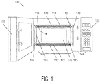
- FIG. 1 is a perspective view of a defrosting system 100, in accordance with an example embodiment.
- Defrosting system 100 includes a defrosting cavity 110 (e.g., cavity 360, 760, 1174, FIGs 3 , 7 , 11 ), a control panel 120, one or more RF signal sources (e.g., RF signal source 320, 720, 1120, FIGs 3 , 7 , 11 ), a power supply (e.g., power supply 326, 726, FIGs 3 , 7 ), a first electrode 170 (e.g., electrode 340, 740, 1170, FIGs 3 , 7 , 11 ), a second electrode 172 (e.g., electrode 750, 1172, FIGs 7 , 11 ), impedance matching circuitry (e.g., circuits 334, 370, 734, 772, 1160, FIGs 3 , 7 , 11 ), power detection circuitry (e.g., power detection circuitry 330, 730
- the defrosting cavity 110 is defined by interior surfaces of top, bottom, side, and back cavity walls 111, 112, 113, 114, 115 and an interior surface of door 116. With door 116 closed, the defrosting cavity 110 defines an enclosed air cavity.
- air cavity may mean an enclosed area that contains air or other gasses (e.g., defrosting cavity 110).
- the first electrode 170 is arranged proximate to a cavity wall (e.g., top wall 111), the first electrode 170 is electrically isolated from the remaining cavity walls (e.g., walls 112-115 and door 116), and the remaining cavity walls are grounded.
- the system may be simplistically modeled as a capacitor, where the first electrode 170 functions as one conductive plate (or electrode), the grounded cavity walls (e.g., walls 112-115) function as a second conductive plate (or electrode), and the air cavity (including any load contained therein) function as a dielectric medium between the first and second conductive plates.
- a non-electrically conductive barrier (e.g., barrier 362, 762, FIGs 3 , 7 ) also may be included in the system 100, and the non-conductive barrier may function to electrically and physically isolate the load from the bottom cavity wall 112.
- FIG. 1 shows the first electrode 170 being proximate to the top wall 111, the first electrode 170 alternatively may be proximate to any of the other walls 112-115, as indicated by electrodes 172-175.
- the first electrode 170 is arranged proximate to a first cavity wall (e.g., top wall 111), a second electrode 172 is arranged proximate to an opposite, second cavity wall (e.g., bottom wall 112), and the first and second electrodes 170, 172 are electrically isolated from the remaining cavity walls (e.g., walls 113-115 and door 116).
- the system also may be simplistically modeled as a capacitor, where the first electrode 170 functions as one conductive plate (or electrode), the second electrode 172 functions as a second conductive plate (or electrode), and the air cavity (including any load contained therein) function as a dielectric medium between the first and second conductive plates.
- a non-electrically conductive barrier (e.g., barrier 762, 1156, FIGs 7 , 11 ) also may be included in the system 100, and the non-conductive barrier may function to electrically and physically isolate the load from the second electrode 172 and the bottom cavity wall 112.
- FIG. 1 shows the first electrode 170 being proximate to the top wall 111, and the second electrode 172 being proximate to the bottom wall 112, the first and second electrodes 170, 172 alternatively may be proximate to other opposite walls (e.g., the first electrode may be electrode 173 proximate to wall 113, and the second electrode may be electrode 174 proximate to wall 114.
- a user may place one or more loads (e.g., food and/or liquids) into the defrosting cavity 110, and optionally may provide inputs via the control panel 120 that specify characteristics of the load(s).
- the specified characteristics may include an approximate mass of the load.
- the specified load characteristics may indicate the material(s) from which the load is formed (e.g., meat, bread, liquid).
- the load characteristics may be obtained in some other way, such as by scanning a barcode on the load packaging or receiving a radio frequency identification (RFID) signal from an RFID tag on or embedded within the load.
- RFID radio frequency identification
- system controller e.g., system controller 312, 712, 1130, FIGs 3 , 7 , 11
- load characteristics may not be entered or received prior to commencement of a defrosting operation, and the system controller may establish a default initial state for the impedance matching network.
- the user may provide an input via the control panel 120.
- the system controller causes the RF signal source(s) (e.g., RF signal source 320, 720, 1120, FIGs 3 , 7 , 11 ) to supply an RF signal to the first electrode 170 in an unbalanced embodiment, or to both the first and second electrodes 170, 172 in a balanced embodiment, and the electrode(s) responsively radiate electromagnetic energy into the defrosting cavity 110.
- the electromagnetic energy increases the thermal energy of the load (i.e., the electromagnetic energy causes the load to warm up).
- the impedance of the load (and thus the total input impedance of the cavity 110 plus load) changes as the thermal energy of the load increases.
- the impedance changes alter the absorption of RF energy into the load, and thus alter the magnitude of reflected power.
- power detection circuitry e.g., power detection circuitry 330, 730, 1180, FIGs 3 , 7 , 11
- continuously or periodically measures the reflected power along a transmission path e.g., transmission path 328, 728, 1148, FIGs 3 , 7 , 11
- the RF signal source e.g., RF signal source 320, 720, 1120, FIGs 3 , 7 , 11
- the system controller e.g., system controller 312, 712, 1130, FIGs 3 , 7 , 11
- the impedance matching network is variable, and based on the reflected power measurements (or both the forward and reflected power measurements), the system controller may alter the state of the impedance matching network during the defrosting operation to increase the absorption of RF power by the load.
- the defrosting system 100 of FIG. 1 is embodied as a counter-top type of appliance.
- the defrosting system 100 also may include components and functionality for performing microwave cooking operations.
- components of a defrosting system may be incorporated into other types of systems or appliances.
- FIG. 2 is a perspective view of a refrigerator/freezer appliance 200 that includes other example embodiments of defrosting systems 210, 220. More specifically, defrosting system 210 is shown to be incorporated within a freezer compartment 212 of the system 200, and defrosting system 220 is shown to be incorporated within a refrigerator compartment 222 of the system.
- An actual refrigerator/freezer appliance likely would include only one of the defrosting systems 210, 220, but both are shown in FIG. 2 to concisely convey both embodiments.
- each of defrosting systems 210, 220 includes a defrosting cavity, a control panel 214, 224, one or more RF signal sources (e.g., RF signal source 320, 720, 1120, FIGs 3 , 7 , 11 ), a power supply (e.g., power supply 326, 726, FIGs 3 , 7 ), a first electrode (e.g., electrode 340, 740, 1170, FIGs 3 , 7 ), a second electrode 172 (e.g., containment structure 366, electrode 750, FIGs 3 , 7 , 11 ), impedance matching circuitry (e.g., circuits 334, 370, 734, 772, 1160, FIGs 3 , 7 , 11 ), power detection circuitry (e.g., power detection circuitry 330, 730, 1180, FIGs 3 , 7 , 11 ), and a system controller (e.g., system controller 312, 712, 11
- the defrosting cavity may be defined by interior surfaces of bottom, side, front, and back walls of a drawer, and an interior top surface of a fixed shelf 216, 226 under which the drawer slides. With the drawer slid fully under the shelf, the drawer and shelf define the cavity as an enclosed air cavity.
- the components and functionalities of the defrosting systems 210, 220 may be substantially the same as the components and functionalities of defrosting system 100, in various embodiments.
- each of the defrosting systems 210, 220 may have sufficient thermal communication with the freezer or refrigerator compartment 212, 222, respectively, in which the system 210, 220 is disposed.
- the load after completion of a defrosting operation, the load may be maintained at a safe temperature (i.e., a temperature at which food spoilage is retarded) until the load is removed from the system 210, 220. More specifically, upon completion of a defrosting operation by the freezer-based defrosting system 210, the cavity within which the defrosted load is contained may thermally communicate with the freezer compartment 212, and if the load is not promptly removed from the cavity, the load may re-freeze.
- the cavity within which the defrosted load is contained may thermally communicate with the refrigerator compartment 222, and if the load is not promptly removed from the cavity, the load may be maintained in a defrosted state at the temperature within the refrigerator compartment 222.
- defrosting systems may be incorporated into systems or appliances having other configurations, as well. Accordingly, the above-described implementations of defrosting systems in a stand-alone appliance, a microwave oven appliance, a freezer, and a refrigerator are not meant to limit use of the embodiments only to those types of systems.
- defrosting systems 100, 200 are shown with their components in particular relative orientations with respect to one another, it should be understood that the various components may be oriented differently, as well.
- the physical configurations of the various components may be different.
- control panels 120, 214, 224 may have more, fewer, or different user interface elements, and/or the user interface elements may be differently arranged.
- a substantially cubic defrosting cavity 110 is illustrated in FIG. 1 , it should be understood that a defrosting cavity may have a different shape, in other embodiments (e.g., cylindrical, and so on).
- defrosting systems 100, 210, 220 may include additional components (e.g., a fan, a stationary or rotating plate, a tray, an electrical cord, and so on) that are not specifically depicted in FIGs 1 , 2 .
- FIG. 3 is a simplified block diagram of an unbalanced defrosting system 300 (e.g., defrosting system 100, 210, 220, FIGs 1 , 2 ), in accordance with an example embodiment.
- Defrosting system 300 includes RF subsystem 310, defrosting cavity 360, user interface 380, system controller 312, RF signal source 320, power supply and bias circuitry 326, variable impedance matching network 370, electrode 340, containment structure 366, and power detection circuitry 330, in an embodiment.
- defrosting system 300 may include temperature sensor(s), and/or infrared (IR) sensor(s) 390, although some or all of these sensor components may be excluded.
- FIG. 3 is a simplified representation of a defrosting system 300 for purposes of explanation and ease of description, and that practical embodiments may include other devices and components to provide additional functions and features, and/or the defrosting system 300 may be part of a larger electrical system.
- User interface 380 may correspond to a control panel (e.g., control panel 120, 214, 224, FIGs 1 , 2 ), for example, which enables a user to provide inputs to the system regarding parameters for a defrosting operation (e.g., characteristics of the load to be defrosted, and so on), start and cancel buttons, mechanical controls (e.g., a door/drawer open latch), and so on.
- the user interface may be configured to provide user-perceptible outputs indicating the status of a defrosting operation (e.g., a countdown timer, visible indicia indicating progress or completion of the defrosting operation, and/or audible tones indicating completion of the defrosting operation) and other information.
- defrosting system 300 may include temperature sensor(s), and/or IR sensor(s) 390.
- the temperature sensor(s) and/or IR sensor(s) may be positioned in locations that enable the temperature of the load 364 to be sensed during the defrosting operation.
- the temperature information enables the system controller 312 to alter the power of the RF signal supplied by the RF signal source 320 (e.g., by controlling the bias and/or supply voltages provided by the power supply and bias circuitry 326), to adjust the state of the variable impedance matching network 370, and/or to determine when the defrosting operation should be terminated.
- the system controller 312 may use this information, for example, to determine a desired power level for the RF signal supplied by the RF signal source 320, to determine an initial setting for the variable impedance matching network 370, and/or to determine an approximate duration for the defrosting operation.
- the RF subsystem 310 includes a system controller 312, an RF signal source 320, first impedance matching circuit 334 (herein “first matching circuit"), power supply and bias circuitry 326, and power detection circuitry 330, in an embodiment.
- System controller 312 may include one or more general purpose or special purpose processors (e.g., a microprocessor, microcontroller, Application Specific Integrated Circuit (ASIC), and so on), volatile and/or non-volatile memory (e.g., Random Access Memory (RAM), Read Only Memory (ROM), flash, various registers, and so on), one or more communication busses, and other components.
- general purpose or special purpose processors e.g., a microprocessor, microcontroller, Application Specific Integrated Circuit (ASIC), and so on
- volatile and/or non-volatile memory e.g., Random Access Memory (RAM), Read Only Memory (ROM), flash, various registers, and so on
- RAM Random Access Memory
- ROM Read Only Memory
- flash various registers, and so
- system controller 312 is coupled to user interface 380, RF signal source 320, variable impedance matching network 370, power detection circuitry 330, and sensors 390 (if included).
- System controller 312 is configured to receive signals indicating user inputs received via user interface 380, and to receive signals indicating RF signal reflected power (and possibly RF signal forward power) from power detection circuitry 330. Responsive to the received signals and measurements, and as will be described in more detail later, system controller 312 provides control signals to the power supply and bias circuitry 326 and to the RF signal generator 322 of the RF signal source 320. In addition, system controller 312 provides control signals to the variable impedance matching network 370, which cause the network 370 to change its state or configuration.
- Defrosting cavity 360 includes a capacitive defrosting arrangement with first and second parallel plate electrodes that are separated by an air cavity within which a load 364 to be defrosted may be placed.
- a first electrode 340 may be positioned above the air cavity, and a second electrode may be provided by a portion of a containment structure 366.
- the containment structure 366 may include bottom, top, and side walls, the interior surfaces of which define the cavity 360 (e.g., cavity 110, FIG. 1 ).
- the cavity 360 may be sealed (e.g., with a door 116, FIG. 1 or by sliding a drawer closed under a shelf 216, 226, FIG.
- the system 300 may include one or more interlock mechanisms that ensure that the seal is intact during a defrosting operation. If one or more of the interlock mechanisms indicates that the seal is breached, the system controller 312 may cease the defrosting operation.
- the containment structure 366 is at least partially formed from conductive material, and the conductive portion(s) of the containment structure may be grounded. Alternatively, at least the portion of the containment structure 366 that corresponds to the bottom surface of the cavity 360 may be formed from conductive material and grounded.
- the containment structure 366 (or at least the portion of the containment structure 366 that is parallel with the first electrode 340) functions as a second electrode of the capacitive defrosting arrangement.
- a non-conductive barrier 362 may be positioned over the bottom surface of the cavity 360.
- defrosting cavity 360 includes a capacitive defrosting arrangement with first and second parallel plate electrodes 340, 366 that are separated by an air cavity within which a load 364 to be defrosted may be placed.
- the first electrode 340 is positioned within containment structure 366 to define a distance 352 between the electrode 340 and an opposed surface of the containment structure 366 (e.g., the bottom surface, which functions as a second electrode), where the distance 352 renders the cavity 360 a sub-resonant cavity, in an embodiment.
- the distance 352 is in a range of about 0.10 meters to about 1.0 meter, although the distance may be smaller or larger, as well. According to an embodiment, distance 352 is less than one wavelength of the RF signal produced by the RF subsystem 310. In other words, as mentioned above, the cavity 360 is a sub-resonant cavity. In some embodiments, the distance 352 is less than about half of one wavelength of the RF signal. In other embodiments, the distance 352 is less than about one quarter of one wavelength of the RF signal. In still other embodiments, the distance 352 is less than about one eighth of one wavelength of the RF signal. In still other embodiments, the distance 352 is less than about one 50th of one wavelength of the RF signal. In still other embodiments, the distance 352 is less than about one 100th of one wavelength of the RF signal.
- a system 300 designed for lower operational frequencies may be designed to have a distance 352 that is a smaller fraction of one wavelength.
- a distance 352 that is a smaller fraction of one wavelength.
- system 300 is designed to produce an RF signal with an operational frequency of about 10 MHz (corresponding to a wavelength of about 30 meters), and distance 352 is selected to be about 0.5 meters, the distance 352 is about one 60th of one wavelength of the RF signal.
- system 300 is designed for an operational frequency of about 300 MHz (corresponding to a wavelength of about 1 meter), and distance 352 is selected to be about 0.5 meters, the distance 352 is about one half of one wavelength of the RF signal.
- the first electrode 340 and the containment structure 366 are capacitively coupled. More specifically, the first electrode 340 may be analogized to a first plate of a capacitor, the containment structure 366 may be analogized to a second plate of a capacitor, and the load 364, barrier 362, and air within the cavity 360 may be analogized to a capacitor dielectric. Accordingly, the first electrode 340 alternatively may be referred to herein as an "anode,” and the containment structure 366 may alternatively be referred to herein as a "cathode.”
- the RF subsystem 310 is configured to generate the RF signal to produce voltages between the electrode 340 and the containment structure 366 in a range of about 90 volts to about 3,000 volts, in one embodiment, or in a range of about 3000 volts to about 10,000 volts, in another embodiment, although the system may be configured to produce lower or higher voltages between the electrode 340 and the containment structure 366, as well.
- the first electrode 340 is electrically coupled to the RF signal source 320 through a first matching circuit 334, a variable impedance matching network 370, and a conductive transmission path, in an embodiment.
- the first matching circuit 334 is configured to perform an impedance transformation from an impedance of the RF signal source 320 (e.g., less than about 10 ohms) to an intermediate impedance (e.g., 50 ohms, 75 ohms, or some other value).
- the conductive transmission path includes a plurality of conductors 328-1, 328-2, and 328-3 connected in series, and referred to collectively as transmission path 328.
- the conductive transmission path 328 is an "unbalanced" path, which is configured to carry an unbalanced RF signal (i.e., a single RF signal referenced against ground).
- one or more connectors may be electrically coupled along the transmission path 328, and the portion of the transmission path 328 between the connectors may comprise a coaxial cable or other suitable connector. Such a connection is shown in FIG. 7 and described later (e.g., including connectors 736, 738 and a conductor 728-3 such as a coaxial cable between the connectors 736, 738).
- variable impedance matching circuit 370 is configured to perform an impedance transformation from the above-mentioned intermediate impedance to an input impedance of defrosting cavity 320 as modified by the load 364 (e.g., on the order of hundreds or thousands of ohms, such as about 1000 ohms to about 4000 ohms or more).
- the variable impedance matching network 370 includes a network of passive components (e.g., inductors, capacitors, resistors).
- variable impedance matching network 370 includes a plurality of fixed-value lumped inductors (e.g., inductors 412-414, FIG. 4A ) that are positioned within the cavity 360 and which are electrically coupled to the first electrode 340.
- variable impedance matching network 370 includes a plurality of variable inductance networks (e.g., networks 410, 411, 500, FIGs 4A , 5A ), which may be located inside or outside of the cavity 360.
- variable impedance matching network 370 includes a plurality of variable capacitance networks (e.g., networks 442, 446, 540, FIG.
- variable inductance or capacitance value provided by each of the variable inductance or capacitance networks is established using control signals from the system controller 312, as will be described in more detail later.
- the amount of RF power that is absorbed by the load 364 may be maintained at a high level despite variations in the load impedance during the defrosting operation.
- RF signal source 326 includes an RF signal generator 322 and a power amplifier (e.g., including one or more power amplifier stages 324, 325).
- RF signal generator 322 is configured to produce an oscillating electrical signal having a frequency in the ISM (industrial, scientific, and medical) band, although the system could be modified to support operations in other frequency bands, as well.
- the RF signal generator 322 may be controlled to produce oscillating signals of different power levels and/or different frequencies, in various embodiments.
- the RF signal generator 322 may produce a signal that oscillates in a range of about 10.0 megahertz (MHz) to about 100 MHz and/or from about 100 MHz to about 3.0 gigahertz (GHz). Some desirable frequencies may be, for example, 13.56 MHz (+/- 5 percent), 27.125 MHz (+/- 5 percent), 40.68 MHz (+/- 5 percent), and 2.45 GHz (+/- 5 percent). In one particular embodiment, for example, the RF signal generator 322 may produce a signal that oscillates in a range of about 40.66 MHz to about 40.70 MHz and at a power level in a range of about 10 decibel-milliwatts (dBm) to about 15 dBm. Alternatively, the frequency of oscillation and/or the power level may be lower or higher.
- dBm decibel-milliwatts
- the power amplifier includes a driver amplifier stage 324 and a final amplifier stage 325.
- the power amplifier is configured to receive the oscillating signal from the RF signal generator 322, and to amplify the signal to produce a significantly higher-power signal at an output of the power amplifier.
- the output signal may have a power level in a range of about 100 watts to about 400 watts or more.
- the gain applied by the power amplifier may be controlled using gate bias voltages and/or drain supply voltages provided by the power supply and bias circuitry 326 to each amplifier stage 324, 325. More specifically, power supply and bias circuitry 326 provides bias and supply voltages to each RF amplifier stage 324, 325 in accordance with control signals received from system controller 312.
- each amplifier stage 324, 325 is implemented as a power transistor, such as a field effect transistor (FET), having an input terminal (e.g., a gate or control terminal) and two current carrying terminals (e.g., source and drain terminals).
- Impedance matching circuits may be coupled to the input (e.g., gate) of the driver amplifier stage 324, between the driver and final amplifier stages 325, and/or to the output (e.g., drain terminal) of the final amplifier stage 325, in various embodiments.
- each transistor of the amplifier stages 324, 325 includes a laterally diffused metal oxide semiconductor FET (LDMOSFET) transistor.
- LDMOSFET laterally diffused metal oxide semiconductor FET
- each transistor may be realized as a gallium nitride (GaN) transistor, another type of MOSFET transistor, a bipolar junction transistor (BJT), or a transistor utilizing another semiconductor technology.
- GaN gallium nitride
- BJT bipolar junction transistor
- the power amplifier arrangement is depicted to include two amplifier stages 324, 325 coupled in a particular manner to other circuit components.
- the power amplifier arrangement may include other amplifier topologies and/or the amplifier arrangement may include only one amplifier stage (e.g., as shown in the embodiment of amplifier 724, FIG. 7 ), or more than two amplifier stages.
- the power amplifier arrangement may include various embodiments of a single-ended amplifier, a Doherty amplifier, a Switch Mode Power Amplifier (SMPA), or another type of amplifier.
- SMPA Switch Mode Power Amplifier
- Defrosting cavity 360 and any load 364 positioned in the defrosting cavity 360 present a cumulative load for the electromagnetic energy (or RF power) that is radiated into the cavity 360 by the first electrode 340. More specifically, the cavity 360 and the load 364 present an impedance to the system, referred to herein as a "cavity plus load impedance.”
- the cavity plus load impedance changes during a defrosting operation as the temperature of the load 364 increases.
- the cavity plus load impedance has a direct effect on the magnitude of reflected signal power along the conductive transmission path 328 between the RF signal source 320 and electrodes 340. In most cases, it is desirable to maximize the magnitude of transferred signal power into the cavity 360, and/or to minimize the reflected-to-forward signal power ratio along the conductive transmission path 328.
- a first matching circuit 334 is electrically coupled along the transmission path 328, in an embodiment.
- the first matching circuit 334 may have any of a variety of configurations.
- the first matching circuit 334 includes fixed components (i.e., components with non-variable component values), although the first matching circuit 334 may include one or more variable components, in other embodiments.
- the first matching circuit 334 may include any one or more circuits selected from an inductance/capacitance (LC) network, a series inductance network, a shunt inductance network, or a combination of bandpass, high-pass and low-pass circuits, in various embodiments.
- the fixed matching circuit 334 is configured to raise the impedance to an intermediate level between the output impedance of the RF signal generator 320 and the cavity plus load impedance.
- the system controller 312 is configured to identify a point in time during a defrosting operation when the rate of change of cavity plus load impedance indicates that the load 364 is approaching 0° Celsius, at which time the system controller 312 may terminate the defrosting operation.
- power detection circuitry 330 is coupled along the transmission path 328 between the output of the RF signal source 320 and the electrode 340.
- the power detection circuitry 330 forms a portion of the RF subsystem 310, and is coupled to the conductor 328-2 between the output of the first matching circuit 334 and the input to the variable impedance matching network 370, in an embodiment.
- the power detection circuitry 330 may be coupled to the portion 328-1 of the transmission path 328 between the output of the RF signal source 320 and the input to the first matching circuit 334, or to the portion 328-3 of the transmission path 328 between the output of the variable impedance matching network 370 and the first electrode 340.
- power detection circuitry 330 is configured to monitor, measure, or otherwise detect the power of the reflected signals traveling along the transmission path 328 between the RF signal source 320 and electrode 340 (i.e., reflected RF signals traveling in a direction from electrode 340 toward RF signal source 320). In some embodiments, power detection circuitry 330 also is configured to detect the power of the forward signals traveling along the transmission path 328 between the RF signal source 320 and the electrode 340 (i.e., forward RF signals traveling in a direction from RF signal source 320 toward electrode 340). Over connection 332, power detection circuitry 330 supplies signals to system controller 312 conveying the magnitudes of the reflected signal power (and the forward signal power, in some embodiments) to system controller 312.
- system controller 312 may calculate a reflected-to-forward signal power ratio, or the S11 parameter, or the VSWR value.
- a reflected-to-forward signal power ratio or the S11 parameter, or the VSWR value.
- system controller 312 orchestrates a process of altering the state of the variable matching network 370 to drive the reflected signal power, the S11 parameter, or the VSWR value toward or below a desired level (e.g., below the reflected signal power threshold, and/or the reflected-to-forward signal power ratio threshold, and/or the VSWR threshold), thus re-establishing an acceptable match and facilitating more optimal energy absorption by the load 364.
- a desired level e.g., below the reflected signal power threshold, and/or the reflected-to-forward signal power ratio threshold, and/or the VSWR threshold
- the system controller 312 may provide control signals over control path 316 to the variable matching circuit 370, which cause the variable matching circuit 370 to vary inductive, capacitive, and/or resistive values of one or more components within the circuit, thus adjusting the impedance transformation provided by the circuit 370.
- Adjustment of the configuration of the variable matching circuit 370 desirably decreases the magnitude of reflected signal power, which corresponds to decreasing the magnitude of the S11 parameter and increasing the power absorbed by the load 364.
- variable impedance matching network 370 is used to match the input impedance of the defrosting cavity 360 plus load 364 to maximize, to the extent possible, the RF power transfer into the load 364.
- the initial impedance of the defrosting cavity 360 and the load 364 may not be known with accuracy at the beginning of a defrosting operation. Further, the impedance of the load 364 changes during a defrosting operation as the load 364 warms up.
- the system controller 312 may provide control signals to the variable impedance matching network 370, which cause modifications to the state of the variable impedance matching network 370.
- variable matching network 370 Non-limiting examples of configurations for the variable matching network 370 are shown in FIGs 4A, 4B , 5A, and 5B .
- the network 370 may include any one or more circuits selected from an inductance/capacitance (LC) network, an inductance-only network, a capacitance-only network, or a combination of bandpass, high-pass and low-pass circuits, in various embodiments.
- the variable matching network 370 includes a single-ended network (e.g., network 400, 440, FIG. 4A, 4B ).
- variable matching network 370 The inductance, capacitance, and/or resistance values provided by the variable matching network 370, which in turn affect the impedance transformation provided by the network 370, are established using control signals from the system controller 312, as will be described in more detail later.
- the system controller 312 controls the state of the variable matching network 370 over the course of a defrosting operation to dynamically match the ever-changing impedance of the cavity 360 plus the load 364 within the cavity 360.
- variable matching network 370 may have any of a wide variety of circuit configurations, and non-limiting examples of such configurations are shown in FIGs 4A, 4B , 5A, and 5B .
- the variable impedance matching network 370 may include a single-ended network of passive components, and more specifically a network of fixed-value inductors (e.g., lumped inductive components) and variable inductors (or variable inductance networks).
- the variable impedance matching network 370 may include a single-ended network of passive components, and more specifically a network of variable capacitors (or variable capacitance networks).
- the term “inductor” means a discrete inductor or a set of inductive components that are electrically coupled together without intervening components of other types (e.g., resistors or capacitors).
- the term “capacitor” means a discrete capacitor or a set of capacitive components that are electrically coupled together without intervening components of other types (e.g., resistors or inductors).
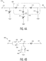
- FIG. 4A is a schematic diagram of a single-ended variable impedance matching network 400 (e.g., variable impedance matching network 370, FIG. 3 ), in accordance with an example embodiment.
- the variable impedance matching network 370 essentially has two portions: one portion to match the RF signal source (or the final stage power amplifier); and another portion to match the cavity plus load.
- Variable impedance matching network 400 includes an input node 402, an output node 404, first and second variable inductance networks 410, 411, and a plurality of fixed-value inductors 412-415, according to an embodiment.
- the input node 402 is electrically coupled to an output of the RF signal source (e.g., RF signal source 320, FIG. 3 )
- the output node 404 is electrically coupled to an electrode (e.g., first electrode 340, FIG. 3 ) within the defrosting cavity (e.g., defrosting cavity 360, FIG. 3 ).
- the variable impedance matching network 400 includes first and second, series coupled lumped inductors 412, 414, in an embodiment.
- the first and second lumped inductors 412, 414 are relatively large in both size and inductance value, in an embodiment, as they may be designed for relatively low frequency (e.g., about 40.66 MHz to about 40.70 MHz) and high power (e.g., about 50 watts (W) to about 500 W) operation.
- inductors 412, 414 may have values in a range of about 200 nanohenries (nH) to about 600 nH, although their values may be lower and/or higher, in other embodiments.
- the first variable inductance network 410 is a first shunt inductive network that is coupled between the input node 402 and a ground reference terminal (e.g., the grounded containment structure 366, FIG. 3 ).
- the first variable inductance network 410 is configurable to match the impedance of the RF signal source (e.g., RF signal source 320, FIG. 3 ) as modified by the first matching circuit (e.g., circuit 334, FIG. 3 ), or more particularly to match the impedance of the final stage power amplifier (e.g., amplifier 325, FIG. 3 ) as modified by the first matching circuit 334 (e.g., circuit 334, FIG. 3 ).
- the first variable inductance network 410 may be referred to as the "RF signal source matching portion" of the variable impedance matching network 400.
- the first variable inductance network 410 includes a network of inductive components that may be selectively coupled together to provide inductances in a range of about 10 nH to about 400 nH, although the range may extend to lower or higher inductance values, as well.
- the "cavity matching portion" of the variable impedance matching network 400 is provided by a second shunt inductive network 416 that is coupled between a node 422 between the first and second lumped inductors 412, 414 and the ground reference terminal.
- the second shunt inductive network 416 includes a third lumped inductor 413 and a second variable inductance network 411 coupled in series, with an intermediate node 422 between the third lumped inductor 413 and the second variable inductance network 411.
- the second shunt inductive network 416 is configurable to optimally match the impedance of the cavity plus load (e.g., cavity 360 plus load 364, FIG. 3 ).
- inductor 413 may have a value in a range of about 400 nH to about 800 nH, although its value may be lower and/or higher, in other embodiments. According to an embodiment, and as will be described in more detail in conjunction with FIG.
- the second variable inductance network 411 includes a network of inductive components that may be selectively coupled together to provide inductances in a range of about 50 nH to about 800 nH, although the range may extend to lower or higher inductance values, as well.
- variable impedance matching network 400 includes a fourth lumped inductor 415 coupled between the output node 404 and the ground reference terminal.
- inductor 415 may have a value in a range of about 400 nH to about 800 nH, although its value may be lower and/or higher, in other embodiments.
- the set 430 of lumped inductors 412-415 may form a portion of a module that is at least partially physically located within the cavity (e.g., cavity 360, FIG. 3 ), or at least within the confines of the containment structure (e.g., containment structure 366, FIG. 3 ). This enables the radiation produced by the lumped inductors 412-415 to be safely contained within the system, rather than being radiated out into the surrounding environment.
- the variable inductance networks 410, 411 may or may not be contained within the cavity or the containment structure, in various embodiments.
- variable impedance matching network 400 embodiment of FIG. 4A includes “only inductors” to provide a match for the input impedance of the defrosting cavity 360 plus load 364.
- the network 400 may be considered an "inductor-only” matching network.
- the phrases “only inductors” or “inductor-only” when describing the components of the variable impedance matching network means that the network does not include discrete resistors with significant resistance values or discrete capacitors with significant capacitance values.
- conductive transmission lines between components of the matching network may have minimal resistances, and/or minimal parasitic capacitances may be present within the network.
- variable impedance matching networks may include differently configured inductor-only matching networks, and matching networks that include combinations of discrete inductors, discrete capacitors, and/or discrete resistors.
- an "inductor-only" matching network alternatively may be defined as a matching network that enables impedance matching of a capacitive load using solely or primarily inductive components.
- FIG. 5A is a schematic diagram of a variable inductance network 500 that may be incorporated into a variable impedance matching network (e.g., as variable inductance networks 410 and/or 411, FIG. 4A ), in accordance with an example embodiment.
- Network 500 includes an input node 530, an output node 532, and a plurality, N , of discrete inductors 501-504 coupled in series with each other between the input and output nodes 530, 532, where N may be an integer between 2 and 10, or more.
- network 500 includes a plurality, N , of bypass switches 511-514, where each switch 511-514 is coupled in parallel across the terminals of one of the inductors 501-504.
- Switches 511-514 may be implemented as transistors, mechanical relays or mechanical switches, for example.
- the electrically conductive state of each switch 511-514 (i.e., open or closed) is controlled through control signals 521-524 from the system controller (e.g., system controller 312, FIG. 3 ).
- This configuration represents the maximum inductance state of the network 500 (i.e., the state of network 500 in which a maximum inductance value is present between input and output nodes 530, 532).
- the trace inductance for the variable inductance network 500 may be in a range of about 10 nH to about 50 nH, although the trace inductance may be smaller or larger, as well. Larger, smaller, or substantially similar trace inductances also may be inherent in each of the other network states, as well, where the trace inductance for any given network state is a summation of the inductances of the sequence of conductors and switches through which the current primarily is carried through the network 500.
- each inductor 501-504 has substantially the same inductance value, referred to herein as a normalized value of I .
- each inductor 501-504 may have a value in a range of about 10 nH to about 200 nH, or some other value.
- the maximum inductance value for the network 500 (i.e., when all switches 511-514 are in an open state) would be about N x I , plus any trace inductance that may be present in the network 500 when it is in the maximum inductance state.
- the inductance value for the network 500 When any n switches are in a closed state, the inductance value for the network 500 would be about ( N -n)x I (plus trace inductance).
- the state of the network 500 may be configured to have any of N +1 values of inductance.
- the inductors 501-504 may have different values from each other.
- the first inductor 501 may have a normalized inductance value of I
- each subsequent inductor 502-504 in the series may have a larger or smaller inductance value.
- each subsequent inductor 502-504 may have an inductance value that is a multiple (e.g., about twice) the inductance value of the nearest downstream inductor 501-503, although the difference may not necessarily be an integer multiple.
- the state of the network 500 may be configured to have any of 2 N values of inductance.
- the network 500 may be configured to have any of 16 values of inductance.
- inductor 501 has a value of I
- inductor 502 has a value of 2 ⁇ I
- inductor 503 has a value of 4 ⁇ I
- inductor 504 has a value of 8 ⁇ I
- Table 1 indicates the total inductance value for all 16 possible states of the network 500 (not accounting for trace inductances): Table 1 ⁇ Total inductance values for all possible variable inductance network states
- Network state Switch 511 state (501 value I )
- Total network inductance (w/o trace inductance) 0 closed closed closed closed 0 1 open closed closed closed I 2 closed open closed closed closed 2x I 3 open open closed closed 3x I
- N 4
- each successive inductor is about twice the inductance of the preceding inductor.
- the values of inductors 501-504 may be, for example, about 30 nH, about 50 nH, about 100 nH, and about 200 nH, respectively.
- variable inductance network 411 if an embodiment of variable inductance network 411 is implemented in the same manner, and assuming that the trace inductance is about 50 nH and the range of inductance values achievable by network 411 is about 50 nH (trace inductance) to about 800 nH, the values of inductors 501-504 may be, for example, about 50 nH, about 100 nH, about 200 nH, and about 400 nH, respectively. Of course, more or fewer than four inductors 501-504 may be included in either variable inductance network 410, 411, and the inductors within each network 410, 411 may have different values.
- variable inductance networks may have more or fewer than four inductors, different relative values for the inductors, a different number of possible network states, and/or a different configuration of inductors (e.g., differently connected sets of parallel and/or series coupled inductors). Either way, by providing a variable inductance network in an impedance matching network of a defrosting system, the system may be better able to match the ever-changing cavity plus load impedance that is present during a defrosting operation.
- FIG. 4B is a schematic diagram of a single-ended variable capacitive matching network 440 (e.g., variable impedance matching network 370, FIG. 3 ), which may be implemented instead of the variable-inductance impedance matching network 400 ( FIG. 4A ), in accordance with an example embodiment.
- Variable impedance matching network 440 includes an input node 402, an output node 404, first and second variable capacitance networks 442, 446, and at least one inductor 454, according to an embodiment.
- the input node 402 is electrically coupled to an output of the RF signal source (e.g., RF signal source 320, FIG. 3 )
- the output node 404 is electrically coupled to an electrode (e.g., first electrode 340, FIG. 3 ) within the defrosting cavity (e.g., defrosting cavity 360, FIG. 3 ).
- the variable impedance matching network 440 includes a first variable capacitance network 442 coupled in series with an inductor 454, and a second variable capacitance network 446 coupled between an intermediate node 451 and a ground reference terminal (e.g., the grounded containment structure 366, FIG. 3 ), in an embodiment.
- the inductor 454 may be designed for relatively low frequency (e.g., about 40.66 MHz to about 40.70 MHz) and high power (e.g., about 50 W to about 500 W) operation, in an embodiment.
- inductor 454 may have a value in a range of about 200 nH to about 600 nH, although its value may be lower and/or higher, in other embodiments.
- inductor 454 is a fixed-value, lumped inductor (e.g., a coil). In other embodiments, the inductance value of inductor 454 may be variable.
- the first variable capacitance network 442 is coupled between the input node 402 and the intermediate node 451, and the first variable capacitance network 442 may be referred to as a "series matching portion" of the variable impedance matching network 440.
- the first variable capacitance network 442 includes a first fixed-value capacitor 443 coupled in parallel with a first variable capacitor 444.
- the first fixed-value capacitor 443 may have a capacitance value in a range of about 1 picofarad (pF) to about 100 pF, in an embodiment. As will be described in more detail in conjunction with FIG.
- the first variable capacitor 444 may include a network of capacitive components that may be selectively coupled together to provide capacitances in a range of 0 pF to about 100 pF. Accordingly, the total capacitance value provided by the first variable capacitance network 442 may be in a range of about 1 pF to about 200 pF, although the range may extend to lower or higher capacitance values, as well.
- a "shunt matching portion" of the variable impedance matching network 440 is provided by the second variable capacitance network 446, which is coupled between node 451 (located between the first variable capacitance network 442 and lumped inductor 454) and the ground reference terminal.
- the second variable capacitance network 446 includes a second fixed-value capacitor 447 coupled in parallel with a second variable capacitor 448.
- the second fixed-value capacitor 447 may have a capacitance value in a range of about 1 pF to about 100 pF, in an embodiment.
- the second variable capacitor 448 may include a network of capacitive components that may be selectively coupled together to provide capacitances in a range of 0 pF to about 100 pF. Accordingly, the total capacitance value provided by the second variable capacitance network 446 may be in a range of about 1 pF to about 200 pF, although the range may extend to lower or higher capacitance values, as well.
- the states of the first and second variable capacitance networks 442, 446 may be changed to provide multiple capacitance values, and thus may be configurable to optimally match the impedance of the cavity plus load (e.g., cavity 360 plus load 364, FIG. 3 ) to the RF signal source (e.g., RF signal source 320, FIG. 3 ).
- FIG. 5B is a schematic diagram of a single-ended variable capacitive network 540 that may be incorporated into a variable impedance matching network (e.g., for each instance of variable capacitors 444, 448, FIG. 4B ), in accordance with an example embodiment.
- Network 540 includes an input node 531, an output node 533, and a plurality, N , of discrete capacitors 541-544 coupled in parallel with each other between the input and output nodes 531, 533, where N may be an integer between 2 and 10, or more.
- network 540 includes a plurality, N, of bypass switches 551-554, where each switch 551-554 is coupled in series with one of the terminals of one of the capacitors 541-544.
- Switches 551-554 may be implemented as transistors, mechanical relays or mechanical switches, for example.
- the electrically conductive state of each switch 551-554 (i.e., open or closed) is controlled through control signals 561-564 from the system controller (e.g., system controller 312, FIG. 3 ).
- the system controller e.g., system controller 312, FIG. 3 .
- a single switch is connected to one of the terminals of each capacitor, and the terminal to which the switch is coupled alternates between a bottom terminal (e.g., for capacitors 541 and 543) and a top terminal (e.g., for capacitors 542 and 544) across the series of parallel-coupled capacitors 541-544.
- the terminal to which the switch is coupled may be the same across the network (e.g., each switch is coupled to a top terminal or to a bottom terminal in each parallel-coupled branch, but not both), or two switches may be coupled to both the top and bottom terminals of each capacitor in each parallel-coupled branch. In the latter embodiment, the two switches coupled to each capacitor may be controlled to open and close in a synchronized manner.
- This configuration represents the maximum capacitance state of the network 540 (i.e., the state of network 540 in which a maximum capacitance value is present between input and output nodes 531, 533).
- This configuration represents the minimum capacitance state of the network 540 (i.e., the state of network 540 in which a minimum capacitance value is present between input and output nodes 531, 533).
- each capacitor 541-544 has substantially the same capacitance value, referred to herein as a normalized value of J.
- each capacitor 541-544 may have a value in a range of about 1 pF to about 25 pF, or some other value.
- the maximum capacitance value for the network 540 i.e., when all switches 551-554 are in a closed state
- the capacitance value for the network 540 would be about ( N -n)x J .
- the state of the network 540 may be configured to have any of N +1 values of capacitance.
- the capacitors 541-544 may have different values from each other. For example, moving from the input node 531 toward the output node 533, the first capacitor 541 may have a normalized capacitance value of J , and each subsequent capacitor 542-544 in the series may have a larger or smaller capacitance value. For example, each subsequent capacitor 542-544 may have a capacitance value that is a multiple (e.g., about twice) the capacitance value of the nearest downstream capacitor 541-543, although the difference may not necessarily be an integer multiple. In such an embodiment, the state of the network 540 may be configured to have any of 2 N values of capacitance.
- the network 540 may be configured to have any of 16 values of capacitance.
- the total capacitance value for all 16 possible states of the network 540 may be represented by a table similar to Table 1, above (except switching the value of I for J , and reversing the "open" and "closed” designations).
- FIG. 6 is an example of a Smith chart 600 depicting how the plurality of inductances in an embodiment of a variable impedance matching network (e.g., network 370, 400, FIGs 3 , 4A ) may match the cavity plus load impedance to the RF signal source.
- a plurality of capacitances in an embodiment of a variable impedance matching network e.g., network 370, 440, FIGs 3 , 4B
- the example Smith chart 600 assumes that the system is a 50 Ohm system, and that the output of the RF signal source is 50 Ohms. Those of skill in the art would understand, based on the description herein, how the Smith chart could be modified for a system and/or RF signal source with different characteristic impedances.
- point 601 corresponds to the point at which the load (e.g., the cavity 360 plus load 364, FIG. 3 ) would locate (e.g., at the beginning of a defrosting operation) absent the matching provided by the variable impedance matching network (e.g., network 370, 400, FIGs 3 , 4A ).
- the load is a capacitive load.
- the shunt and series inductances of the variable impedance matching network sequentially move the substantially-capacitive load impedance toward an optimal matching point 606 (e.g., 50 Ohms) at which RF energy transfer to the load may occur with minimal losses.
- shunt inductance 415 moves the impedance to point 602
- series inductance 414 moves the impedance to point 603
- shunt inductance 416 moves the impedance to point 604
- series inductance 412 moves the impedance to point 605
- shunt inductance 410 moves the impedance to the optimal matching point 606.
- an alternate definition of an "inductor-only" matching network may be a matching network that enables impedance matching of a capacitive load using solely or primarily inductive components, where the impedance matching network performs the transformation substantially within the lower right quadrant of the Smith chart.
- variable impedance matching network As discussed previously, the impedance of the load changes during the defrosting operation. Accordingly, point 601 correspondingly moves during the defrosting operation. Movement of load point 601 is compensated for, according to the previously-described embodiments, by varying the impedance of the first and second shunt inductances 410, 411 so that the final match provided by the variable impedance matching network still may arrive at or near the optimal matching point 606.
- a specific variable impedance matching network has been illustrated and described herein, those of skill in the art would understand, based on the description herein, that differently-configured variable impedance matching networks may achieve the same or similar results to those conveyed by Smith chart 600.
- variable impedance matching network may have more or fewer shunt and/or series inductances, and or different ones of the inductances may be configured as variable inductance networks (e.g., including one or more of the series inductances). Accordingly, although a particular variable inductance matching network has been illustrated and described herein, the inventive subject matter is not limited to the illustrated and described embodiment.
- FIGs 3-6 discuss, in detail, an "unbalanced" defrosting apparatus, in which an RF signal is applied to one electrode (e.g., electrode 340, FIG. 3 ), and the other "electrode” (e.g., the containment structure 366, FIG. 3 ) is grounded.
- an alternate embodiment of a defrosting apparatus comprises a "balanced” defrosting apparatus. In such an apparatus, balanced RF signals are provided to both electrodes.
- FIG. 7 is a simplified block diagram of a balanced defrosting system 700 (e.g., defrosting system 100, 210, 220, FIGs 1 , 2 ), in accordance with an example embodiment.
- Defrosting system 700 includes RF subsystem 710, defrosting cavity 760, user interface 780, system controller 712, RF signal source 720, power supply and bias circuitry 726, variable impedance matching network 770, two electrodes 740, 750, and power detection circuitry 730, in an embodiment.
- defrosting system 700 may include temperature sensor(s), and/or infrared (IR) sensor(s) 790, although some or all of these sensor components may be excluded.
- FIG. 7 is a simplified representation of a defrosting system 700 for purposes of explanation and ease of description, and that practical embodiments may include other devices and components to provide additional functions and features, and/or the defrosting system 700 may be part of a larger electrical system.
- User interface 780 may correspond to a control panel (e.g., control panel 120, 214, 224, FIGs 1 , 2 ), for example, which enables a user to provide inputs to the system regarding parameters for a defrosting operation (e.g., characteristics of the load to be defrosted, and so on), start and cancel buttons, mechanical controls (e.g., a door/drawer open latch), and so on.
- the user interface may be configured to provide user-perceptible outputs indicating the status of a defrosting operation (e.g., a countdown timer, visible indicia indicating progress or completion of the defrosting operation, and/or audible tones indicating completion of the defrosting operation) and other information.
- the RF subsystem 710 includes a system controller 712, an RF signal source 720, a first impedance matching circuit 734 (herein “first matching circuit"), power supply and bias circuitry 726, and power detection circuitry 730, in an embodiment.
- System controller 712 may include one or more general purpose or special purpose processors (e.g., a microprocessor, microcontroller, ASIC, and so on), volatile and/or non-volatile memory (e.g., RAM, ROM, flash, various registers, and so on), one or more communication busses, and other components.
- system controller 712 is operatively and communicatively coupled to user interface 780, RF signal source 720, power supply and bias circuitry 726, power detection circuitry 730 (or 730' or 730"), variable matching subsystem 770, sensor(s) 790 (if included), and pump 792 (if included).
- System controller 712 is configured to receive signals indicating user inputs received via user interface 780, to receive signals indicating RF signal reflected power (and possibly RF signal forward power) from power detection circuitry 730 (or 730' or 730"), and to receive sensor signals from sensor(s) 790.
- system controller 712 Responsive to the received signals and measurements, and as will be described in more detail later, system controller 712 provides control signals to the power supply and bias circuitry 726 and/or to the RF signal generator 722 of the RF signal source 720. In addition, system controller 712 provides control signals to the variable matching subsystem 770 (over path 716), which cause the subsystem 770 to change the state or configuration of a variable impedance matching circuit 772 of the subsystem 770 (herein "variable matching circuit").
- Defrosting cavity 760 includes a capacitive defrosting arrangement with first and second parallel plate electrodes 740, 750 that are separated by an air cavity within which a load 764 to be defrosted may be placed.
- first and second electrodes 740, 750 e.g., electrodes 140, 150, FIG. 1
- an interior defrosting cavity 760 e.g., interior cavity 260, FIG. 2
- a distance 752 between the electrodes 740, 750 renders the cavity 760 a sub-resonant cavity, in an embodiment.
- the first and second electrodes 740, 750 are separated across the cavity 760 by a distance 752.
- the distance 752 is in a range of about 0.10 meters to about 1.0 meter, although the distance may be smaller or larger, as well.
- distance 752 is less than one wavelength of the RF signal produced by the RF subsystem 710.
- the cavity 760 is a sub-resonant cavity.
- the distance 752 is less than about half of one wavelength of the RF signal.
- the distance 752 is less than about one quarter of one wavelength of the RF signal.
- the distance 752 is less than about one eighth of one wavelength of the RF signal.
- the distance 752 is less than about one 50th of one wavelength of the RF signal.
- the distance 752 is less than about one 100th of one wavelength of the RF signal.
- a system 700 designed for lower operational frequencies may be designed to have a distance 752 that is a smaller fraction of one wavelength.
- a distance 752 that is a smaller fraction of one wavelength.
- system 700 is designed to produce an RF signal with an operational frequency of about 10 MHz (corresponding to a wavelength of about 30 meters), and distance 752 is selected to be about 0.5 meters, the distance 752 is about one 60th of one wavelength of the RF signal.
- system 700 is designed for an operational frequency of about 300 MHz (corresponding to a wavelength of about 1 meter), and distance 752 is selected to be about 0.5 meters, the distance 752 is about one half of one wavelength of the RF signal.
- the first and second electrodes 740, 750 are capacitively coupled. More specifically, the first electrode 740 may be analogized to a first plate of a capacitor, the second electrode 750 may be analogized to a second plate of a capacitor, and the load 764, barrier 762, and air within the cavity 760 may be analogized to a capacitor dielectric. Accordingly, the first electrode 740 alternatively may be referred to herein as an "anode,” and the second electrode 750 may alternatively be referred to herein as a "cathode.”
- the voltage across the first and second electrodes 740, 750 heats the load 764 within the cavity 760.
- the RF subsystem 710 is configured to generate the RF signal to produce voltages across the electrodes 740, 750 in a range of about 70 volts to about 3000 volts, in one embodiment, or in a range of about 3000 volts to about 10,000 volts, in another embodiment, although the system may be configured to produce lower or higher voltages across electrodes 740, 750, as well.
- the conductive transmission path 728 includes an "unbalanced" portion and a "balanced" portion, where the "unbalanced" portion is configured to carry an unbalanced RF signal (i.e., a single RF signal referenced against ground), and the "balanced" portion is configured to carry a balanced RF signal (i.e., two signals referenced against each other).
- the "unbalanced" portion of the transmission path 728 may include unbalanced first and second conductors 728-1, 728-2 within the RF subsystem 710, one or more connectors 736, 738 (each having male and female connector portions), and an unbalanced third conductor 728-3 electrically coupled between the connectors 736, 738.
- the third conductor 728-3 comprises a coaxial cable, although the electrical length may be shorter or longer, as well.
- the variable matching subsystem 770 may be housed with the RF subsystem 710, and in such an embodiment, the conductive transmission path 728 may exclude the connectors 736, 738 and the third conductor 728-3.
- the "balanced" portion of the conductive transmission path 728 includes a balanced fourth conductor 728-4 within the variable matching subsystem 770, and a balanced fifth conductor 728-5 electrically coupled between the variable matching subsystem 770 and electrodes 740, 750, in an embodiment.
- the variable matching subsystem 770 houses an apparatus configured to receive, at an input of the apparatus, the unbalanced RF signal from the RF signal source 720 over the unbalanced portion of the transmission path (i.e., the portion that includes unbalanced conductors 728-1, 728-2, and 728-3), to convert the unbalanced RF signal into two balanced RF signals (e.g., two RF signals having a phase difference between 120 and 240 degrees, such as about 180 degrees), and to produce the two balanced RF signals at two outputs of the apparatus.
- the conversion apparatus may be a balun 774, in an embodiment.
- the balanced RF signals are conveyed over balanced conductors 728-4 to the variable matching circuit 772 and, ultimately, over balanced conductors 728-5 to the electrodes 740, 750.
- an alternate RF signal generator 720' may produce balanced RF signals on balanced conductors 728-1', which may be directly coupled to the variable matching circuit 772 (or coupled through various intermediate conductors and connectors).
- the balun 774 may be excluded from the system 700.
- a double-ended variable matching circuit 772 (e.g., variable matching circuit 800, 900, 1000, FIGs 8-10 ) is configured to receive the balanced RF signals (e.g., over connections 728-4 or 728-1'), to perform an impedance transformation corresponding to a then-current configuration of the double-ended variable matching circuit 772, and to provide the balanced RF signals to the first and second electrodes 740, 750 over connections 728-5.
- the balanced RF signals e.g., over connections 728-4 or 728-1'
- RF signal source 720 includes an RF signal generator 722 and a power amplifier 724 (e.g., including one or more power amplifier stages).
- RF signal generator 722 is configured to produce an oscillating electrical signal having a frequency in an ISM (industrial, scientific, and medical) band, although the system could be modified to support operations in other frequency bands, as well.
- the RF signal generator 722 may be controlled to produce oscillating signals of different power levels and/or different frequencies, in various embodiments.
- the RF signal generator 722 may produce a signal that oscillates in a range of about 10.0 MHz to about 100 MHz and/or from about 100 MHz to about 3.0 GHz.
- Some desirable frequencies may be, for example, 13.56 MHz (+/- 5 percent), 27.125 MHz (+/- 5 percent), 40.68 MHz (+/- 5 percent), and 2.45 GHz (+/- 5 percent).
- the frequency of oscillation may be lower or higher than the above-given ranges or values.
- the power amplifier 724 is configured to receive the oscillating signal from the RF signal generator 722, and to amplify the signal to produce a significantly higher-power signal at an output of the power amplifier 724.
- the output signal may have a power level in a range of about 100 watts to about 400 watts or more, although the power level may be lower or higher, as well.
- the gain applied by the power amplifier 724 may be controlled using gate bias voltages and/or drain bias voltages provided by the power supply and bias circuitry 726 to one or more stages of amplifier 724. More specifically, power supply and bias circuitry 726 provides bias and supply voltages to the inputs and/or outputs (e.g., gates and/or drains) of each RF amplifier stage in accordance with control signals received from system controller 712.
- the power amplifier may include one or more amplification stages.
- each stage of amplifier 724 is implemented as a power transistor, such as a FET, having an input terminal (e.g., a gate or control terminal) and two current carrying terminals (e.g., source and drain terminals).
- Impedance matching circuits may be coupled to the input (e.g., gate) and/or output (e.g., drain terminal) of some or all of the amplifier stages, in various embodiments.
- each transistor of the amplifier stages includes an LDMOS FET.
- each transistor is not intended to be limited to any particular semiconductor technology, and in other embodiments, each transistor may be realized as a GaN transistor, another type of MOS FET transistor, a BJT, or a transistor utilizing another semiconductor technology.
- the power amplifier arrangement 724 is depicted to include one amplifier stage coupled in a particular manner to other circuit components.
- the power amplifier arrangement 724 may include other amplifier topologies and/or the amplifier arrangement may include two or more amplifier stages (e.g., as shown in the embodiment of amplifier 324/325, FIG. 3 ).
- the power amplifier arrangement may include various embodiments of a single-ended amplifier, a double-ended (balanced) amplifier, a push-pull amplifier, a Doherty amplifier, a Switch Mode Power Amplifier (SMPA), or another type of amplifier.
- SMPA Switch Mode Power Amplifier
- an alternate RF signal generator 720' may include a push-pull or balanced amplifier 724', which is configured to receive, at an input, an unbalanced RF signal from the RF signal generator 722, to amplify the unbalanced RF signal, and to produce two balanced RF signals at two outputs of the amplifier 724', where the two balanced RF signals are thereafter conveyed over conductors 728-1' to the electrodes 740, 750.
- the balun 774 may be excluded from the system 700, and the conductors 728-1' may be directly connected to the variable matching circuit 772 (or connected through multiple coaxial cables and connectors or other multi-conductor structures).
- Defrosting cavity 760 and any load 764 positioned in the defrosting cavity 760 present a cumulative load for the electromagnetic energy (or RF power) that is radiated into the interior chamber 762 by the electrodes 740, 750. More specifically, and as described previously, the defrosting cavity 760 and the load 764 present an impedance to the system, referred to herein as a "cavity plus load impedance.”
- the cavity plus load impedance changes during a defrosting operation as the temperature of the load 764 increases.
- the cavity plus load impedance has a direct effect on the magnitude of reflected signal power along the conductive transmission path 728 between the RF signal source 720 and the electrodes 740, 750. In most cases, it is desirable to maximize the magnitude of transferred signal power into the cavity 760, and/or to minimize the reflected-to-forward signal power ratio along the conductive transmission path 728.
- a first matching circuit 734 is electrically coupled along the transmission path 728, in an embodiment.
- the first matching circuit 734 is configured to perform an impedance transformation from an impedance of the RF signal source 720 (e.g., less than about 10 ohms) to an intermediate impedance (e.g., 50 ohms, 75 ohms, or some other value).
- the first matching circuit 734 may have any of a variety of configurations. According to an embodiment, the first matching circuit 734 includes fixed components (i.e., components with non-variable component values), although the first matching circuit 734 may include one or more variable components, in other embodiments.
- the first matching circuit 734 may include any one or more circuits selected from an inductance/capacitance (LC) network, a series inductance network, a shunt inductance network, or a combination of bandpass, high-pass and low-pass circuits, in various embodiments.
- the first matching circuit 734 is configured to raise the impedance to an intermediate level between the output impedance of the RF signal generator 720 and the cavity plus load impedance.
- power detection circuitry 730 is coupled along the transmission path 728 between the output of the RF signal source 720 and the electrodes 740, 750.
- the power detection circuitry 730 forms a portion of the RF subsystem 710, and is coupled to the conductor 728-2 between the RF signal source 720 and connector 736.
- the power detection circuitry 730 may be coupled to any other portion of the transmission path 728, such as to conductor 728-1, to conductor 728-3, to conductor 728-4 between the RF signal source 720 (or balun 774) and the variable matching circuit 772 (i.e., as indicated with power detection circuitry 730'), or to conductor 728-5 between the variable matching circuit 772 and the electrode(s) 740, 750 (i.e., as indicated with power detection circuitry 730").
- the power detection circuitry is referred to herein with reference number 730, although the circuitry may be positioned in other locations, as indicated by reference numbers 730' and 730".
- power detection circuitry 730 is configured to monitor, measure, or otherwise detect the power of the reflected signals traveling along the transmission path 728 between the RF signal source 720 and one or both of the electrode(s) 740, 750 (i.e., reflected RF signals traveling in a direction from electrode(s) 740, 750 toward RF signal source 720). In some embodiments, power detection circuitry 730 also is configured to detect the power of the forward signals traveling along the transmission path 728 between the RF signal source 720 and the electrode(s) 740, 750 (i.e., forward RF signals traveling in a direction from RF signal source 720 toward electrode(s) 740, 750).
- power detection circuitry 730 supplies signals to system controller 712 conveying the measured magnitudes of the reflected signal power, and in some embodiments, also the measured magnitude of the forward signal power. In embodiments in which both the forward and reflected signal power magnitudes are conveyed, system controller 712 may calculate a reflected-to-forward signal power ratio, or the S11 parameter, or the VSWR value.
- the reflected signal power magnitude exceeds a reflected signal power threshold, or when the reflected-to-forward signal power ratio exceeds an S11 parameter threshold, or when the VSWR value exceeds a VSWR threshold, this indicates that the system 700 is not adequately matched to the cavity plus load impedance, and that energy absorption by the load 764 within the cavity 760 may be sub-optimal.
- system controller 712 orchestrates a process of altering the state of the variable matching circuit 772 to drive the reflected signal power or the S11 parameter or the VSWR value toward or below a desired level (e.g., below the reflected signal power threshold, and/or the reflected-to-forward signal power ratio threshold, and/or a VSWR threshold), thus re-establishing an acceptable match and facilitating more optimal energy absorption by the load 764.
- a desired level e.g., below the reflected signal power threshold, and/or the reflected-to-forward signal power ratio threshold, and/or a VSWR threshold
- the system controller 712 may provide control signals over control path 716 to the variable matching circuit 772, which cause the variable matching circuit 772 to vary inductive, capacitive, and/or resistive values of one or more components within the circuit, thus adjusting the impedance transformation provided by the circuit 772.
- Adjustment of the configuration of the variable matching circuit 772 desirably decreases the magnitude of reflected signal power, which corresponds to decreasing the magnitude of the S11 parameter and increasing the power absorbed by the load 764.
- variable matching circuit 772 is used to match the input impedance of the defrosting cavity 760 plus load 764 to maximize, to the extent possible, the RF power transfer into the load 764.
- the initial impedance of the defrosting cavity 760 and the load 764 may not be known with accuracy at the beginning of a defrosting operation. Further, the impedance of the load 764 changes during a defrosting operation as the load 764 warms up.
- the system controller 712 may provide control signals to the variable matching circuit 772, which cause modifications to the state of the variable matching circuit 772.
- the variable matching circuit 772 may have any of a variety of configurations.
- the circuit 772 may include any one or more circuits selected from an inductance/capacitance (LC) network, an inductance-only network, a capacitance-only network, or a combination of bandpass, high-pass and low-pass circuits, in various embodiments.
- the variable matching circuit 772 is implemented in a balanced portion of the transmission path 728, the variable matching circuit 772 is a double-ended circuit with two inputs and two outputs.
- variable matching circuit may be a single-ended circuit with a single input and a single output (e.g., similar to matching circuit 400 or 440, FIGs 4A, 4B ).
- the variable matching circuit 772 includes a variable inductance network (e.g., double-ended network 800, 900, FIGs 8, 9 ).
- the variable matching circuit 772 includes a variable capacitance network (e.g., double-ended network 1000, FIG. 10 ).
- the variable matching circuit 772 may include both variable inductance and variable capacitance elements.
- variable matching circuit 772 which in turn affect the impedance transformation provided by the circuit 772, are established through control signals from the system controller 712, as will be described in more detail later.
- the system efficiency may be maintained at a high level throughout the defrosting operation.
- the variable matching circuit 772 may have any of a wide variety of circuit configurations, and non-limiting examples of such configurations are shown in FIGs 8-10 .
- FIG. 8 is a schematic diagram of a double-ended variable impedance matching circuit 800 that may be incorporated into a defrosting system (e.g., system 100, 200, 700, FIGs 1 , 2 , 7 ), in accordance with an example embodiment.
- the variable matching circuit 800 includes a network of fixed-value and variable passive components.
- Circuit 800 includes a double-ended input 801-1, 801-2 (referred to as input 801), a double-ended output 802-1, 802-2 (referred to as output 802), and a network of passive components connected in a ladder arrangement between the input 801 and output 802.
- the first input 801-1 may be connected to a first conductor of balanced conductor 728-4
- the second input 801-2 may be connected to a second conductor of balanced conductor 728-4
- the first output 802-1 may be connected to a first conductor of balanced conductor 728-5
- the second output 802-2 may be connected to a second conductor of balanced conductor 728-5.
- circuit 800 includes a first variable inductor 811 and a first fixed inductor 815 connected in series between input 801-1 and output 802-1, a second variable inductor 816 and a second fixed inductor 820 connected in series between input 801-2 and output 802-2, a third variable inductor 821 connected between inputs 801-1 and 801-2, and a third fixed inductor 824 connected between nodes 825 and 826.
- the third variable inductor 821 corresponds to an "RF signal source matching portion", which is configurable to match the impedance of the RF signal source (e.g., RF signal source 720, FIG. 7 ) as modified by the first matching circuit (e.g., circuit 734, FIG. 7 ), or more particularly to match the impedance of the final stage power amplifier (e.g., amplifier 724, FIG. 7 ) as modified by the first matching circuit (e.g., circuit 734, FIG. 7 ).
- the first matching circuit e.g., circuit 734, FIG. 7
- the final stage power amplifier e.g., amplifier 724, FIG. 7
- the third variable inductor 821 includes a network of inductive components that may be selectively coupled together to provide inductances in a range of about 5 nH to about 200 nH, although the range may extend to lower or higher inductance values, as well.
- the "cavity matching portion" of the variable impedance matching network 800 is provided by the first and second variable inductors 811, 816, and fixed inductors 815, 820, and 824. Because the states of the first and second variable inductors 811, 816 may be changed to provide multiple inductance values, the first and second variable inductors 811, 816 are configurable to optimally match the impedance of the cavity plus load (e.g., cavity 760 plus load 764, FIG. 7 ). For example, inductors 811, 816 each may have a value in a range of about 10 nH to about 200 nH, although their values may be lower and/or higher, in other embodiments.
- the fixed inductors 815, 820, 824 also may have inductance values in a range of about 50 nH to about 800 nH, although the inductance values may be lower or higher, as well.
- Inductors 811, 815, 816, 820, 821, 824 may include discrete inductors, distributed inductors (e.g., printed coils), wirebonds, transmission lines, and/or other inductive components, in various embodiments.
- variable inductors 811 and 816 are operated in a paired manner, meaning that their inductance values during operation are controlled to be equal to each other, at any given time, in order to ensure that the RF signals conveyed to outputs 802-1 and 802-2 are balanced.
- variable matching circuit 800 is a double-ended circuit that is configured to be connected along a balanced portion of the transmission path 728 (e.g., between connectors 728-4 and 728-5), and other embodiments may include a single-ended (i.e., one input and one output) variable matching circuit that is configured to be connected along the unbalanced portion of the transmission path 728.
- the system controller 712 may increase or decrease the impedance transformation provided by circuit 800. Desirably, the inductance value changes improve the overall impedance match between the RF signal source 720 and the cavity plus load impedance, which should result in a reduction of the reflected signal power and/or the reflected-to-forward signal power ratio. In most cases, the system controller 712 may strive to configure the circuit 800 in a state in which a maximum electromagnetic field intensity is achieved in the cavity 760, and/or a maximum quantity of power is absorbed by the load 764, and/or a minimum quantity of power is reflected by the load 764.
- FIG. 9 is a schematic diagram of a double-ended variable impedance matching network 900, in accordance with another example embodiment.
- Network 900 includes a double-ended input 901-1, 901-2 (referred to as input 901), a double-ended output 902-1, 902-2 (referred to as output 902), and a network of passive components connected in a ladder arrangement between the input 901 and output 902.
- the ladder arrangement includes a first plurality, N, of discrete inductors 911-914 coupled in series with each other between input 901-1 and output 902-1, where N may be an integer between 2 and 10, or more.
- the ladder arrangement also includes a second plurality, N, of discrete inductors 916-919 coupled in series with each other between input 901-2 and output 902-2.
- Additional discrete inductors 915 and 920 may be coupled between intermediate nodes 925, 926 and the output nodes 902-1, 902-2. Further still, the ladder arrangement includes a third plurality of discrete inductors 921-923 coupled in series with each other between inputs 901-1 and 901-2, and an additional discrete inductor 924 coupled between nodes 925 and 926.
- the fixed inductors 915, 920, 924 each may have inductance values in a range of about 50 nH to about 800 nH, although the inductance values may be lower or higher, as well.
- the series arrangement of inductors 911-914 may be considered a first variable inductor (e.g., inductor 811, FIG. 8 ), the series arrangement of inductors 916-919 may be considered a second variable inductor (e.g., inductor 816, FIG. 8 ), and series arrangement of inductors 921-923 may be considered a third variable inductor (e.g., inductor 821, FIG. 8 ).
- network 900 includes a plurality of bypass switches 931-934, 936-939, 941, and 943, where each switch 931-934, 936-939, 941, and 943 is coupled in parallel across the terminals of one of inductors 911-914, 916-919, 921, and 923.
- Switches 931-934, 936-939, 941, and 943 may be implemented as transistors, mechanical relays or mechanical switches, for example.
- each switch 931-934, 936-939, 941, and 943 i.e., open or closed
- control signals 951-954, 956-959, 961, 963 from the system controller e.g., control signals from system controller 712 provided over connection 716, FIG. 7 .
- sets of corresponding inductors in the two paths between input 901 and output 902 have substantially equal values, and the conductive state of the switches for each set of corresponding inductors is operated in a paired manner, meaning that the switch states during operation are controlled to be the same as each other, at any given time, in order to ensure that the RF signals conveyed to outputs 902-1 and 902-2 are balanced.
- inductors 911 and 916 may constitute a first "set of corresponding inductors” or “paired inductors” with substantially equal values, and during operation, the states of switches 931 and 936 are controlled to be the same (e.g., either both open or both closed), at any given time.
- inductors 912 and 917 may constitute a second set of corresponding inductors with equal inductance values that are operated in a paired manner
- inductors 913 and 918 may constitute a third set of corresponding inductors with equal inductance values that are operated in a paired manner
- inductors 914 and 919 may constitute a fourth set of corresponding inductors with equal inductance values that are operated in a paired manner.
- This configuration represents the maximum inductance state of the network 900 (i.e., the state of network 900 in which a maximum inductance value is present between input and output nodes 901, 902).
- the switches 931-934, 936-939, 941, and 943 are closed, substantially all current flowing between input and output nodes 901, 902 bypasses the inductors 911-914 and 916-919 and flows instead through the switches 931-934 or 936-939, inductors 915 or 920, and the conductive interconnections between the input and output nodes 901, 902 and switches 931-934, 936-939.
- This configuration represents the minimum inductance state of the network 900 (i.e., the state of network 900 in which a minimum inductance value is present between input and output nodes 901, 902).
- the minimum inductance value would be near zero inductance.
- a relatively small inductance is present in the minimum inductance state due to the cumulative inductances of the switches 931-934 or 936-939, inductors 915 or 920, and the conductive interconnections between nodes 901, 902 and the switches 931-934 or 936-939.
- a trace inductance for the series combination of switches 931-934 or 936-939 may be in a range of about 10 nH to about 400 nH, although the trace inductance may be smaller or larger, as well. Larger, smaller, or substantially similar trace inductances also may be inherent in each of the other network states, as well, where the trace inductance for any given network state is a summation of the inductances of the sequence of conductors and switches through which the current primarily is carried through the network 900.
- the system controller may provide control signals 951-954, 956-959 that result in the closure of any combination of switches 931-934, 936-939 in order to reduce the inductance of the network 900 by bypassing corresponding combinations of inductors 911-914, 916-919.
- each inductor 911-914, 916-919 has substantially the same inductance value, referred to herein as a normalized value of I .
- each inductor 911-914, 916-919 may have a value in a range of about 1 nH to about 400 nH, or some other value.
- the maximum inductance value between input node 901-1 and 902-2, and the maximum inductance value between input node 901-2 and 902-2 i.e., when all switches 931-934, 936-939 are in an open state
- the inductance value between corresponding input and output nodes would be about ( N -n) ⁇ I (plus trace inductance).
- the inductors 911-914, 916-919 may have different values from each other.
- the first inductor 911 may have a normalized inductance value of I
- each subsequent inductor 912-914 in the series may have a larger or smaller inductance value.
- the first inductor 916 may have a normalized inductance value of I
- each subsequent inductor 917-919 in the series may have a larger or smaller inductance value.
- each subsequent inductor 912-914 or 917-919 may have an inductance value that is a multiple (e.g., about twice or half) the inductance value of the nearest downstream inductor 911-914 or 916-918.
- Table 1, above applies also to the first series inductance path between input and output nodes 901-1 and 902-1, and the second series inductance path between input and output nodes 901-2 and 902-1.
- inductor/switch combinations 911/931 and 916/956 each are analogous to inductor/switch combination 501/511
- inductor/switch combinations 912/932 and 917/957 each are analogous to inductor/switch combination 502/512
- inductor/switch combinations 913/933 and 918/958 each are analogous to inductor/switch combination 503/513
- inductor/switch combinations 914/934 and 919/959 each are analogous to inductor/switch combination 504/514.
- the values of inductors 911-914 may be, for example, about 10 nH, about 20 nH, about 40 nH, about 80 nH, and about 160 nH, respectively.
- the combination of series inductors 916-919 may be similarly or identically configured.
- inductors 911-914 or 916-919 may be included in either series combination between input and output nodes 901-1/902-1 or 901-2/902-2, and the inductors within each series combination may have different values from the example values given above.
- variable series inductance networks may have more or fewer than four inductors, different relative values for the inductors, and/or a different configuration of inductors (e.g., differently connected sets of parallel and/or series coupled inductors). Either way, by providing a variable inductance network in an impedance matching network of a defrosting system, the system may be better able to match the ever-changing cavity plus load impedance that is present during a defrosting operation.
- the third plurality of discrete inductors 921-923 corresponds to an "RF signal source matching portion" of the circuit.
- the third variable inductor comprises the series arrangement of inductors 921-923, where bypass switches 941 and 943 enable inductors 921 and 923 selectively to be connected into the series arrangement or bypassed based on control signals 961 and 963.
- each of inductors 921-923 may have equal values (e.g., values in a range of about 1 nH to about 100 nH. In an alternate embodiment, the inductors 921-923 may have different values from each other.
- Inductor 922 is electrically connected between input terminals 901-1 and 901-2 regardless of the state of bypass switches 941 and 943. Accordingly, the inductance value of inductor 922 serves as a baseline (i.e., minimum) inductance between input terminals 901-1 and 901-2.
- the first and third inductors 921, 923 may have inductance values that are a ratio of each other. For example, when the first inductor 921 has a normalized inductance value of J , inductor 923 may have a value of 2 ⁇ J, 3 ⁇ J, 4 ⁇ J, or some other ratio, in various embodiments.
- FIG. 10 is a schematic diagram of a double-ended variable impedance matching circuit 1000 that may be incorporated into a defrosting system (e.g., system 100, 200, 700, FIGs 1 , 2 , 7 ), in accordance with another example embodiment.
- the variable matching circuit 1000 includes a network of fixed-value and variable passive components.
- Circuit 1000 includes a double-ended input 1001-1, 1001-2 (referred to as input 1001), a double-ended output 1002-1, 1002-2 (referred to as output 1002), and a network of passive components connected between the input 1001 and output 1002.
- the first input 1001-1 may be connected to a first conductor of balanced conductor 728-4
- the second input 1001-2 may be connected to a second conductor of balanced conductor 728-4
- the first output 1002-1 may be connected to a first conductor of balanced conductor 728-5
- the second output 1002-2 may be connected to a second conductor of balanced conductor 728-5.
- circuit 1000 includes a first variable capacitance network 1011 and a first inductor 1015 connected in series between input 1001-1 and output 1002-1, a second variable capacitance network 1016 and a second inductor 1020 connected in series between input 1001-2 and output 1002-2, and a third variable capacitance network 1021 connected between nodes 1025 and 1026.
- the inductors 1015, 1020 are relatively large in both size and inductance value, in an embodiment, as they may be designed for relatively low frequency (e.g., about 40.66 MHz to about 40.70 MHz) and high power (e.g., about 50 W to about 500 W) operation.
- inductors 1015, 1020 each may have a value in a range of about 100 nH to about 1000 nH (e.g., in a range of about 200 nH to about 600 nH), although their values may be lower and/or higher, in other embodiments.
- inductors 1015, 1020 are fixed-value, lumped inductors (e.g., coils, discrete inductors, distributed inductors (e.g., printed coils), wirebonds, transmission lines, and/or other inductive components, in various embodiments).
- the inductance value of inductors 1015, 1020 may be variable.
- inductance values of inductors 1015, 1020 are substantially the same either permanently (when inductors 1015, 1020 are fixed-value) or at any given time (when inductors 1015, 1020 are variable, they are operated in a paired manner), in an embodiment.
- the first and second variable capacitance networks 1011, 1016 correspond to "series matching portions" of the circuit 1000.
- the first variable capacitance network 1011 includes a first fixed-value capacitor 1012 coupled in parallel with a first variable capacitor 1013.
- the first fixed-value capacitor 1012 may have a capacitance value in a range of about 1 pF to about 100 pF, in an embodiment.
- the first variable capacitor 1013 may include a network of capacitive components that may be selectively coupled together to provide capacitances in a range of 0 pF to about 100 pF. Accordingly, the total capacitance value provided by the first variable capacitance network 1011 may be in a range of about 1 pF to about 200 pF, although the range may extend to lower or higher capacitance values, as well.
- the second variable capacitance network 1016 includes a second fixed-value capacitor 1017 coupled in parallel with a second variable capacitor 1018.
- the second fixed-value capacitor 1017 may have a capacitance value in a range of about 1 pF to about 100 pF, in an embodiment.
- the second variable capacitor 1018 may include a network of capacitive components that may be selectively coupled together to provide capacitances in a range of 0 pF to about 100 pF. Accordingly, the total capacitance value provided by the second variable capacitance network 1016 may be in a range of about 1 pF to about 200 pF, although the range may extend to lower or higher capacitance values, as well.
- the capacitance values of the first and second variable capacitance networks 1011, 1016 are controlled to be substantially the same at any given time, in an embodiment.
- the capacitance values of the first and second variable capacitors 1013, 1018 may be controlled so that the capacitance values of the first and second variable capacitance networks 1011, 1016 are substantially the same at any given time.
- the first and second variable capacitors 1013, 1018 are operated in a paired manner, meaning that their capacitance values during operation are controlled, at any given time, to ensure that the RF signals conveyed to outputs 1002-1 and 1002-2 are balanced.
- the capacitance values of the first and second fixed-value capacitors 1012, 1017 may be substantially the same, in some embodiments, although they may be different, in others.
- the "shunt matching portion" of the variable impedance matching network 1000 is provided by the third variable capacitance network 1021 and fixed inductors 1015, 1020.
- the third variable capacitance network 1021 includes a third fixed-value capacitor 1023 coupled in parallel with a third variable capacitor 1024.
- the third fixed-value capacitor 1023 may have a capacitance value in a range of about 1 pF to about 500 pF, in an embodiment.
- the third variable capacitor 1024 may include a network of capacitive components that may be selectively coupled together to provide capacitances in a range of 0 pF to about 200 pF. Accordingly, the total capacitance value provided by the third variable capacitance network 1021 may be in a range of about 1 pF to about 700 pF, although the range may extend to lower or higher capacitance values, as well.
- variable capacitance networks 1011, 1016, 1021 are configurable to optimally match the impedance of the cavity plus load (e.g., cavity 760 plus load 764, FIG. 7 ) to the RF signal source (e.g., RF signal source 720, 720', FIG. 7 ).
- the system controller e.g., system controller 712, FIG. 7
- the impedance transformation provided by circuit 1000.
- the capacitance value changes improve the overall impedance match between the RF signal source 720 and the impedance of the cavity plus load, which should result in a reduction of the reflected signal power and/or the reflected-to-forward signal power ratio.
- the system controller 712 may strive to configure the circuit 1000 in a state in which a maximum electromagnetic field intensity is achieved in the cavity 760, and/or a maximum quantity of power is absorbed by the load 764, and/or a minimum quantity of power is reflected by the load 764.
- variable impedance matching circuits 800, 900, 100 illustrated in FIGs 8-10 are but three possible circuit configurations that may perform the desired double-ended variable impedance transformations.
- Other embodiments of double-ended variable impedance matching circuits may include differently arranged inductive or capacitive networks, or may include passive networks that include various combinations of inductors, capacitors, and/or resistors, where some of the passive components may be fixed-value components, and some of the passive components may be variable-value components (e.g., variable inductors, variable capacitors, and/or variable resistors).
- the double-ended variable impedance matching circuits may include active devices (e.g., transistors) that switch passive components into and out of the network to alter the overall impedance transformation provided by the circuit.
- FIG. 11 is a cross-sectional, side view of a defrosting system 1100, in accordance with an example embodiment.
- the defrosting system 1100 generally includes a defrosting cavity 1174, a user interface (not shown), a system controller 1130, an RF signal source 1120, power supply and bias circuitry (not shown), power detection circuitry 1180, a variable impedance matching network 1160, a first electrode 1170, and a second electrode 1172, in an embodiment.
- the system controller 1130, RF signal source 1120, power supply and bias circuitry, and power detection circuitry 1180 may form portions of a first module (e.g., RF module 1300, FIG. 13 ), and the variable impedance matching network 1160 may form portions of a second module (e.g., either module 1200 or 1240, FIGs 12A, 12B ).
- defrosting system 1100 may include temperature sensor(s), and/or IR sensor(s) 1192.
- the defrosting system 1100 is contained within a containment structure 1150, in an embodiment.
- the containment structure 1150 may define two or more interior areas, such as the defrosting cavity 1174 and a circuit housing area 1178.
- the containment structure 1150 includes bottom, top, and side walls. Portions of the interior surfaces of some of the walls of the containment structure 1150 may define the defrosting cavity 1174.
- the defrosting cavity 1174 includes a capacitive defrosting arrangement with first and second parallel plate electrodes 1170, 1172 that are separated by an air cavity within which a load 1164 to be defrosted may be placed.
- the first electrode 1170 may be positioned above the air cavity, and a second electrode 1172 may be, in the single-ended system embodiment, provided by a conductive portion of the containment structure 1150 (e.g., a portion of the bottom wall of the containment structure 1150).
- the second electrode 1172 may be formed from a conductive plate, as shown, that is distinct from the containment structure 1150.
- non-electrically conductive support structure(s) 1154 may be employed to suspend the first electrode 1170 above the air cavity, to electrically isolate the first electrode 1170 from the containment structure 1150, and to hold the first electrode 1170 in a fixed physical orientation with respect to the air cavity.
- a nonconductive support and barrier structure 1156 may be positioned over the bottom surface of the containment structure 1150.
- the containment structure 1150 is at least partially formed from conductive material, and the conductive portion(s) of the containment structure may be grounded to provide a ground reference for various electrical components of the system.
- the conductive portion(s) of the containment structure may be grounded to provide a ground reference for various electrical components of the system.
- at least the portion of the containment structure 1150 that corresponds to the second electrode 1172 may be formed from conductive material and grounded.
- the temperature sensor(s) and/or IR sensor(s) 1192 may be positioned in locations that enable the temperature of the load 1164 to be sensed both before, during, and after a defrosting operation. According to an embodiment, the temperature sensor(s) and/or IR sensor(s) 1192 are configured to provide load temperature estimates to the system controller 1130.
- Some or all of the various components of the system controller 1130, the RF signal source 1120, the power supply and bias circuitry (not shown), the power detection circuitry 1180, and the variable impedance matching network 1160 may be coupled to one or more common substrates (e.g., substrate 1152) within the circuit housing area 1178 of the containment structure 1150, in an embodiment.
- substrate 1152 e.g., substrate 1152
- some of all of the above-listed components may be included in an RF module (e.g., RF module 1300, FIG. 13 ) and a variable impedance matching circuit module (e.g., a variation of module 1200 or 1240, FIGs 12A, 12B ), which are housed within the circuit housing area 1178 of the containment structure 1150.
- the system controller 1130 is coupled to the user interface, RF signal source 1120, variable impedance matching network 1160, and power detection circuitry 1180 through various conductive interconnects on or within the common substrate 1152, and/or through various cables (e.g., coaxial cables), not shown.
- the power detection circuitry 1180 is coupled along the transmission path 1148 between the output of the RF signal source 1120 and the input to the variable impedance matching network 1160, in an embodiment.
- the substrate 1152 may include a microwave or RF laminate, a polytetrafluorethylene (PTFE) substrate, a printed circuit board (PCB) material substrate (e.g., FR-4), an alumina substrate, a ceramic tile, or another type of substrate.
- PTFE polytetrafluorethylene
- PCB printed circuit board
- various ones of the components may be coupled to different substrates with electrical interconnections between the substrates and components.
- some or all of the components may be coupled to a cavity wall, rather than being coupled to a distinct substrate.
- the first electrode 1170 is electrically coupled to the RF signal source 1120 through a variable impedance matching network 1160 and a transmission path 1148, in an embodiment.
- the second electrode 1172 also is electrically coupled to the RF signal source 1120 through a variable impedance matching network 1160 and a transmission path 1148.
- single-ended embodiments of the variable impedance matching network 1160 may include a single-ended variable inductance network (e.g., network 400, FIG. 4A ) or a single-ended variable capacitance network (e.g., network 440, FIG. 4B ).
- variable impedance matching network 1160 may include a double-ended variable inductance network (e.g., network 800, 900, FIGs 8, 9 ) or a double-ended variable capacitance network (e.g., network 1000, FIG. 10 ).
- the variable impedance matching network 1160 is implemented as a module (e.g., one of modules 1200, 1240, FIGs 12A, 12B ), or is coupled to the common substrate 1152 and located within the circuit housing area 1178.
- Conductive structures e.g., conductive vias, traces, cables, wires, and other structures
- the circuitry associated with the single-ended or double-ended variable impedance matching networks discussed herein may be implemented in the form of one or more modules, where a "module" is defined herein as an assembly of electrical components coupled to a common substrate.
- FIGs 12A and 12B are a perspective views of examples of modules 1200, 1240 that include a double-ended variable impedance matching network (e.g., networks 800, 900, 1000, FIGs 8-10 ), in accordance with two example embodiments.
- FIG 12A illustrates a module 1200 that houses a variable inductance impedance matching network (e.g., networks 800, 900, FIGs 8, 9 ), and FIG 12B illustrates a module 1240 that houses a variable capacitance impedance matching network (e.g., network 1000, FIG. 10 ).
- a variable inductance impedance matching network e.g., networks 800, 900, FIGs 8, 9
- FIG 12B illustrates a module 1240 that houses a variable capacitance impedance matching network (e.g., network 1000, FIG. 10 ).
- Each of the modules 1200, 1240 includes a printed circuit board (PCB) 1204, 1244 with a front side 1206, 1246 and an opposite back side 1208, 1248.
- the PCB 1204, 1244 is formed from one or more dielectric layers, and two or more printed conductive layers. Conductive vias (not visible in FIGs 12A, 12B ) may provide for electrical connections between the multiple conductive layers.
- a plurality of printed conductive traces formed from a first printed conductive layer provides for electrical connectivity between the various components that are coupled to the front side 1206, 1246 of the PCB 1204, 1244.
- a plurality of printed conductive traces formed from a second printed conductive layer provides for electrical connectivity between the various components that are coupled to the back side 1208, 1248 of the PCB 1204, 1244.
- each PCB 1204, 1244 houses an RF input connector 1238, 1278 (e.g., coupled to back side 1208, 1248 and thus not visible in the views of FIGs 12A, 12B , but corresponding to connector 738, FIG. 7 ) and a balun 1274, 1284 (e.g., coupled to back side 1208, 1248 and thus not visible in the view of FIGs 12A, 12B , but corresponding to balun 774, FIG. 7 ).
- the input connector 1238, 1278 is configured to be electrically connected to an RF subsystem (e.g., subsystem 310, 710, FIGs 3 , 7 ) with a connection (e.g., connection 728-3, FIG.
- an unbalanced RF signal received by the balun 1274, 1284 from the RF input connector 1238, 1278 is converted to a balanced signal, which is provided over a pair of balanced conductors (e.g., connections 728-4, FIG. 7 ) to a double-ended input that includes first and second inputs 1201-1, 1201-2 or 1241-1, 1242-2.
- the connection between the input connector 1238, 1278 and the balun 1274, 1284, and the connections between the balun 1274, 1284 and the inputs 1201-1, 1201-2, 1241-1, 1241-2 each may be implemented using conductive traces and vias formed on and in the PCB 1204, 1244.
- an alternate embodiment may include a balanced amplifier (e.g., balanced amplifier 724', FIG. 7 ), which produces a balanced signal on connections (e.g., conductors 728-1', FIG. 7 ) that can be directly coupled to the inputs 1201-1, 1201-2, 1241-1, 1241-2.
- the balun 1274, 1284 may be excluded from the module 1200, 1240.
- each PCB 1204, 1244 houses circuitry associated with a double-ended variable impedance matching network (e.g., network 772, 800, 900, 1000, FIGs 7-10 ).
- a double-ended variable impedance matching network e.g., network 772, 800, 900, 1000, FIGs 7-10 .
- the circuitry housed by the PCB 1204 includes the double-ended input 1201-1, 1201-2 (e.g., inputs 901-1, 901-2, FIG. 9 ), a double-ended output 1202-1, 1202-2 (e.g., outputs 902-1, 902-2, FIG.
- a first plurality of inductors 1211, 1212, 1213, 1214, 1215 (e.g., inductors 911-915, FIG. 9 ) coupled in series between a first input 1201-1 of the double-ended input and a first output 1202-1 of the double-ended output
- a second plurality of inductors 1216, 1217, 1218, 1219, 1220 (e.g., inductors 916-920, FIG 9 ) coupled in series between a second input 1201-2 of the double-ended input and a second output 1202-2 of the double-ended output
- a third plurality of inductors (not visible in the view of FIG. 12 , but corresponding to inductors 921-923, FIG.
- inductor 924 (e.g., inductor 924, FIG. 9 ) coupled between nodes 1225 and 1226 (e.g., nodes 925, 926).
- a plurality of switches or relays also are coupled to the PCB 1204.
- the plurality of switches or relays may be coupled to the front side 1206 or to the back side 1208 of the PCB 1204.
- Each of the switches or relays is electrically connected in parallel across one of the inductors 1211-1214, 1216-1219, or one of the inductors (e.g., inductors 921, 923, FIG. 9 ) between inputs 1202-1 and 1202-2, in an embodiment.
- a control connector 1230 is coupled to the PCB 1204, and conductors of the control connector 1230 are electrically coupled to conductive traces 1232 to provide control signals to the switches (e.g., control signals 951-954, 956-959, 961, 963, FIG. 9 ), and thus to switch the inductors into or out of the circuit, as described previously.
- switches e.g., control signals 951-954, 956-959, 961, 963, FIG. 9
- fixed-value inductors 1215, 1220 e.g., inductors 915, 920, FIG. 9
- the conductive features corresponding to outputs 1202-1, 1202-2 may be relatively large, and may be elongated for direct attachment to the electrodes (e.g., electrodes 740, 750, FIG. 7 ) of the system.
- the circuitry housed by the PCB 1244 includes a double-ended input 1241-1, 1241-2 (e.g., inputs 1001-1, 1001-2, FIG. 10 ), a double-ended output 1242-1, 1242-2 (e.g., outputs 1002-1, 1002-2, FIG. 10 ), a first plurality of capacitors 1251, 1252 (e.g., capacitors 1012, 1013, FIG. 10 ) that comprise a first variable capacitance network (e.g., network 1011, FIG.
- a double-ended input 1241-1, 1241-2 e.g., inputs 1001-1, 1001-2, FIG. 10
- a double-ended output 1242-1, 1242-2 e.g., outputs 1002-1, 1002-2, FIG. 10
- a first plurality of capacitors 1251, 1252 e.g., capacitors 1012, 1013, FIG. 10
- a first variable capacitance network e.g., network 1011, FIG.
- a second plurality of capacitors 1256, 1257 e.g., capacitors 1017, 1018, FIG 10
- a second variable capacitance network e.g., network 1016, FIG. 10
- a second intermediate node 1266 e.g., node 1026, FIG. 10
- a third plurality of capacitors 1258, 1259 e.g., capacitors 1023, 1024, FIG.
- nodes 1265, 1266 e.g., nodes 1025, 1026
- additional inductors 1255, 1260 e.g., inductors 1015, 1020, FIG 10
- nodes 1265 and 1266 outputs 1242-1, 1242-2.
- the first, second, and third pluralities of capacitors each include a fixed capacitor 1251, 1256, 1258 (e.g., capacitors 1012, 1017, 1023, FIG. 10 ), and a set of one or more capacitors 1252, 1257, 1259 that make up a variable capacitor (e.g., variable capacitors 1013, 1018, 1024).
- Each set of variable capacitors 1252, 1257, 1259 may be implemented using a capacitive network, such as network 500, FIG. 5 .
- a plurality of switches or relays (e.g., not visible in the view of FIG. 12B , but corresponding to switches 551-554, FIG. 5 , for example) also are coupled to the PCB 1244.
- the plurality of switches or relays may be coupled to the front side 1246 or to the back side 1248 of the PCB 1244.
- Each of the switches or relays is electrically connected in series with a terminal of a different one of the capacitors associated with the variable capacitors 1252, 1257, 1259.
- a control connector 1290 is coupled to the PCB 1244, and conductors of the control connector (not shown in FIG. 12B ) are electrically coupled to conductive traces within PCB 1244 to provide control signals to the switches (e.g., control signals 561-564, FIG. 5 ), and thus to switch the capacitors into or out of the circuit, as described previously.
- fixed-value inductors 1255, 1260 are electrically coupled between intermediate nodes 1265 and 1266 and outputs 1242-1, 1242-2.
- the inductors 1255, 1260 may be formed from relatively large coils, although they may be implemented using other structures as well.
- the conductive features corresponding to outputs 1242-1, 1242-2 may be relatively large, and may be elongated for direct attachment to the electrodes (e.g., electrodes 740, 750, FIG. 7 ) of the system. According to an embodiment, and as illustrated in FIG.
- the inductors 1255, 1260 are arranged so that their primary axes are perpendicular to each other (i.e., the axes extending through the centers of the inductors 1255, 1260 are at about 90 degree angles). This may result in significantly reduced electromagnetic coupling between the inductors 1255, 1260.
- the inductors 1255, 1260 may be arranged so that their primary axes are parallel, or may be arranged with other angular offsets.
- FIG. 13 is a perspective view of an RF module 1300 that includes an RF subsystem (e.g., RF subsystem 310, 710, FIGs 3 , 7 ), in accordance with an example embodiment.
- the RF module 1300 includes a PCB 1302 coupled to a ground substrate 1304.
- the ground substrate 1304 provides structural support for the PCB 1302, and also provides an electrical ground reference and heat sink functionality for the various electrical components coupled to the PCB 1302.
- the PCB 1302 houses the circuitry associated with the RF subsystem (e.g., subsystem 310 or 710, FIGs 3 , 7 ).
- the circuitry housed by the PCB 1302 includes system controller circuitry 1312 (e.g., corresponding to system controller 312, 712, FIGs 3 , 7 ), RF signal source circuitry 1320 (e.g., corresponding to RF signal source 320, 720, FIGs 3 , 7 , including an RF signal generator 322, 722 and power amplifier 324, 325, 724), power detection circuitry 1330 (e.g., corresponding to power detection circuitry 330, 730, FIGs 3 , 7 ), and impedance matching circuitry 1334 (e.g., corresponding to first matching circuitry 334, 734, FIGs 3 , 7 ).
- system controller circuitry 1312 e.g., corresponding to system controller 312, 712, FIGs 3 , 7
- RF signal source circuitry 1320 e.g.,
- the system controller circuitry 1312 includes a processor IC and a memory IC
- the RF signal source circuitry 1320 includes a signal generator IC and one or more power amplifier devices
- the power detection circuitry 1330 includes a power coupler device
- the impedance matching circuitry 1334 includes a plurality of passive components (e.g., inductors 1335, 1336 and capacitors 1337) connected together to form an impedance matching network.
- the circuitry 1312, 1320, 1330, 1334 and the various sub-components may be electrically coupled together through conductive traces on the PCB 1302 as discussed previously in reference to the various conductors and connections discussed in conjunction with FIGs 3 , 7 .
- RF module 1300 also includes a plurality of connectors 1316, 1326, 1338, 1380, in an embodiment.
- connector 1380 may be configured to connect with a host system that includes a user interface (e.g., user interface 380, 780, FIGs 3 , 7 ) and other functionality.
- Connector 1316 may be configured to connect with a variable matching circuit (e.g., circuit 372, 772, FIGs 3 , 7 ) to provide control signals to the circuit, as previously described.
- Connector 1326 may be configured to connect to a power supply to receive system power.
- connector 1338 may be configured to connect to a coaxial cable or other transmission line, which enables the RF module 1300 to be electrically connected (e.g., through a coaxial cable implementation of conductor 328-2, 728-3, FIGs 3 , 7 ) to a variable matching subsystem (e.g., subsystem 370, 770, FIGs 3 , 7 ).
- a variable matching subsystem e.g., subsystem 370, 770, FIGs 3 , 7
- components of the variable matching subsystem e.g., variable matching network 370, balun 774, and/or variable matching circuit 772, FIGs 3 , 7
- connector 1336 may be excluded from the module 1300.
- Other variations in the layout, subsystems, and components of RF module 1300 may be made, as well.
- Embodiments of an RF module (e.g., module 1300, FIG. 13 ) and a variable impedance matching network module (e.g., module 1200, 1240, FIGs 12A, 12B ) may be electrically connected together, and connected with other components, to form a defrosting apparatus or system (e.g., apparatus 100, 200, 300, 700, 1100, FIGs 1-3 , 7 , 11 ).
- a defrosting apparatus or system e.g., apparatus 100, 200, 300, 700, 1100, FIGs 1-3 , 7 , 11 .
- an RF signal connection may be made through a connection (e.g., conductor 728-3, FIG. 7 ), such as a coaxial cable, between the RF connector 1338 ( FIG. 13 ) and the RF connector 1238 ( FIG. 12A ) or RF connector 1278 ( FIG.
- connections may be made through connections (e.g., conductors 716, FIG. 7 ), such as a multi-conductor cable, between the connector 1316 ( FIG. 13 ) and the connector 1230 ( FIG. 12A ) or connector 1290 ( FIG. 12B ).
- a host system or user interface may be connected to the RF module 1300 through connector 1380, a power supply may be connected to the RF module 1300 through connector 1326, and electrodes (e.g., electrodes 740, 750, FIG. 7 ) may be connected to the outputs 1202-1, 1202-2 ( FIG. 12A ) or 1242-1, 1242-2 ( FIG. 12B ).
- the above-described assembly also would be physically connected to various support structures and other system components so that the electrodes are held in a fixed relationship to each other across a defrosting cavity (e.g., cavity 110, 360, 760, FIGs 1 , 3 , 7 ), and the defrosting apparatus may be integrated within a larger system (e.g., systems 100, 200, FIGs 1 , 2 ).
- a defrosting cavity e.g., cavity 110, 360, 760, FIGs 1 , 3 , 7
- the defrosting apparatus may be integrated within a larger system (e.g., systems 100, 200, FIGs 1 , 2 ).
- FIG. 14 is a flowchart of a method of operating a defrosting system (e.g., system 100, 210, 220, 300, 700, 1100, FIGs 1-3 , 7 , 11 ) with dynamic load matching, in accordance with an example embodiment.
- a defrosting system e.g., system 100, 210, 220, 300, 700, 1100, FIGs 1-3 , 7 , 11
- dynamic load matching e.g., system 100, 210, 220, 300, 700, 1100, FIGs 1-3 , 7 , 11
- the method may begin, in block 1402, when the system controller (e.g., system controller 312, 712, 1130, FIGs 3 , 7 , 11 ) receives an indication that a defrosting operation should start.
- a defrosting operation e.g., a defrosting operation should start.
- a load e.g., load 364, 764, 1164, FIGs 3 , 7 , 11
- the system's defrosting cavity e.g., cavity 360, 760, 1174, FIGs 3 , 7 , 11
- has sealed the cavity e.g., by closing a door or drawer
- a start button e.g., of the user interface 380, 780, FIGs 3 , 7 ).
- sealing of the cavity may engage one or more safety interlock mechanisms, which when engaged, indicate that RF power supplied to the cavity will not substantially leak into the environment outside of the cavity.
- disengagement of a safety interlock mechanism may cause the system controller immediately to pause or terminate the defrosting operation.
- the system controller optionally may receive additional inputs indicating the load type (e.g., meats, liquids, or other materials), the initial load temperature, and/or the load mass.
- the load type e.g., meats, liquids, or other materials
- information regarding the load type may be received from the user through interaction with the user interface (e.g., by the user selecting from a list of recognized load types).
- the system may be configured to scan a barcode visible on the exterior of the load, or to receive an electronic signal from an RFID device on or embedded within the load.
- Information regarding the initial load temperature may be received, for example, from one or more temperature sensors and/or IR sensors (e.g., sensors 390, 792, 790, 1192, FIGs 3 , 7 , 11 ) of the system.
- Information regarding the initial load temperature may be received from the user through interaction with the user interface, or from one or more temperature sensors and/or IR sensors (e.g., sensor 390, 790, 1192, FIGs 3 , 7 , 11 ) of the system. As indicated above, receipt of inputs indicating the load type, initial load temperature, and/or load mass is optional, and the system alternatively may not receive some or all of these inputs.
- the system controller provides control signals to the variable matching network (e.g., network 370, 400, 440, 772, 800, 900, 1000, 1160, FIGs 3 , 4A, 4B , 7-11 ) to establish an initial configuration or state for the variable matching network that provides a best or acceptable impedance match to the cavity of the defrosting system containing the load.
- the variable matching network e.g., network 370, 400, 440, 772, 800, 900, 1000, 1160, FIGs 3 , 4A, 4B , 7-11
- control signals affect the values of various inductances and/or capacitances (e.g., inductances 410, 411, 414, 811, 816, 821, FIGs 4A , 8 , and capacitances 444, 448, 1013, 1018, 1024, FIGs 4B , 10 ) within the variable matching network.
- inductances 410, 411, 414, 811, 816, 821, FIGs 4A , 8 and capacitances 444, 448, 1013, 1018, 1024, FIGs 4B , 10
- control signals may affect the states of bypass switches (e.g., switches 511-514, 551-554, 931-934, 936-939, 941, 943, FIGs 5A, 5B , 9 ), which are responsive to the control signals from the system controller (e.g., control signals 521-524, 561-564, 951-954, 956-959, 961, 963, FIGs 5A, 5B , 9 ).
- bypass switches e.g., switches 511-514, 551-554, 931-934, 936-939, 941, 943, FIGs 5A, 5B , 9
- the system controller e.g., control signals 521-524, 561-564, 951-954, 956-959, 961, 963, FIGs 5A, 5B , 9 ).
- the system controller adjusts the configuration of the variable impedance matching network to find an acceptable or best match based on actual measurements that are indicative of the quality of the match. Specifically, the system controller causes the RF signal source to supply a relatively low power RF signal through the variable impedance matching network to the electrode(s) (e.g., first electrode 340 or both electrodes 740, 750, 1170, 1172, FIGs 3 , 7 , 11 ).
- the electrode(s) e.g., first electrode 340 or both electrodes 740, 750, 1170, 1172, FIGs 3 , 7 , 11 .
- the system controller may control the RF signal power level through control signals to the power supply and bias circuitry (e.g., circuitry 326, 726, FIGs 3 , 7 ), where the control signals cause the power supply and bias circuitry to provide supply and bias voltages to the amplifiers (e.g., amplifier stages 324, 325, 724, FIGs 3 , 7 ) that are consistent with a desired signal power level.
- the relatively low power RF signal may be a signal having a power level in a range of about 10 W to about 20 W, although different power levels alternatively may be used.
- Supplying a relatively low power level signal may be desirable to reduce the risk of damaging the cavity and/or load (e.g., if the initial match causes high reflected power), and to reduce the risk of damaging the switching components of the variable inductance or capacitance networks (e.g., due to arcing across the switch contacts).
- Power detection circuitry (e.g., power detection circuitry 330, 730, 1180, FIGs 3 , 7 , 11 ) then measures the reflected and (in some embodiments) forward power along the transmission path (e.g., path 328, 728, 1148, FIGs 3 , 7 , 11 ) between the RF signal source and the electrode(s), and provides those measurements to the system controller.
- the system controller may then determine a ratio between the reflected and forward signal powers, and may determine the S11 parameter (e.g., corresponding to return loss) and/or the VSWR value for the system based on the ratio.
- the system controller may store the received power measurements (e.g., the received reflected power measurements, the received forward power measurement, or both), and/or the calculated ratios, and/or S11 parameters, and/or VSWR values for future evaluation or comparison, in an embodiment.
- the system controller may then determine, based on the reflected power measurements, and/or the reflected-to-forward signal power ratio, and/or the S11 parameter, and/or the VSWR value, whether or not the match provided by the variable impedance matching network at the evaluation time is acceptable (e.g., the reflected power is below a threshold, or the reflected-to-forward signal power ratio is 10 percent or less (or below some other threshold), or the measurements or values compare favorably with some other criteria).
- the system controller may be configured to determine whether the match is the "best" match.
- a "best" match may be determined, for example, by iteratively measuring the reflected RF power (and in some embodiments the forward reflected RF power) for all possible impedance matching network configurations (or at least for a defined subset of impedance matching network configurations), and determining which configuration results in the lowest reflected RF power and/or the lowest reflected-to-forward power ratio.
- a binary search algorithm or a regional search algorithm may instead be used to identify the "best match" configuration that results in the lowest reflected RF power and/or the lowest reflected-to-forward power ratio, which may reduce the amount of time needed to find the best match configuration.
- the system controller may adjust the match by reconfiguring the variable impedance matching network. For example, this reconfiguration may be achieved by sending control signals to the variable impedance matching network, which cause the network to increase and/or decrease the variable inductances and/or variable capacitances within the network (e.g., by causing the variable inductance networks 410, 411, 415, 811, 816, 821 ( FIGs 4A , 8 ) or variable capacitance networks 422, 444, 446, 448, 1011, 1013, 1016, 1018, 1021, 1024 ( FIGs 4B , 10 ) to have different inductance or capacitance states, or by switching inductors 501-504, 911-914, 916-919, 921, 923, ( FIGs 5A , 9 ) or capacitors 541-544 ( FIG.
- this reconfiguration may be achieved by sending control signals to the variable impedance matching network, which cause the network to increase and/or decrease the variable inductances and/or variable capacitance
- variable inductance networks e.g., inductance values of inductors 410, 411, 415, 811, 816, 821, FIGs 4A , 8
- capacitance values or states of variable capacitance networks e.g., capacitance values of capacitors 442, 444, 446, 448, 1011, 1013, 1016, 1018, 1021, 1024, FIG. 4B , 10
- in the variable impedance matching network may be stored in a memory of the system controller.
- the system controller uses the initial configuration of the variable impedance network to determine an initial defrosting stage duration and a final defrosting stage duration for the defrosting operation. This may involve the controller comparing the variable impedance matching network configuration to entries within one or more tables, which may be stored in the memory of the system controller and/or memory otherwise accessible to the system controller, in order to determine the initial and final defrosting stage durations.
- An example table may include a plurality of entries, where each entry includes a field for the variable impedance matching network configuration, a field for an initial defrosting stage duration, and a field for a final defrosting stage duration.
- Each entry in the table may include additional fields to provide a description of a typical load associated with the variable impedance matching network configuration as well as a power level (or levels) to be utilized by the defrosting system during the defrosting operation.
- the power levels may be different for the initial defrosting stage and for the final defrosting stage, in some embodiments.
- the configuration of the table may depend at least in part on the configuration of the variable impedance matching network utilized in the system.
- a typical variable impedance matching network may have 30 or more different configurations, where each configuration is associated with a different impedance transformation of the impedance matching network.
- the table may have up to 30 different entries, where each entry in the table is associated with a particular configuration of the impedance matching network and different initial and final defrosting stage durations.
- FIG. 16 shows an illustrative example of a portion of a table 1600 relating initial and final defrosting stage durations to particular configurations of an impedance matching network for an example defrosting system.
- Table 1600 includes a plurality of columns 1602, 1604, 1606, 1608, and 1610, and a plurality of rows or entries 1622, 1624, 1626, 1628, 1630, 1632, 1634, and 1636 where only a subset of the rows/entries may be illustrated in FIG. 16 .
- the intersection of each column and row is referred to herein as a "cell" of the table 1600.
- the cells in column 1602 identify a particular configuration of the defrosting system's impedance matching network or a particular range or grouping of configurations.
- the cells of column 1604 identify a power level of the RF signal to be generated by the RF signal generator (e.g., signal source 320 or 720) of the defrosting system during a defrosting operation.
- the cells in column 1606 identify an initial defrosting stage duration expressed in seconds (though in other embodiments, the initial defrosting stage duration value may be stored using alternative units describing a time or duration).
- the cells in column 1608 identify a final defrosting stage duration expressed in seconds (though in other embodiments, the final defrosting stage duration value may be stored using alternative units describing a time or duration).
- the final defrosting stage duration may specify a duration that is 5% or greater than the initial defrosting stage duration.
- the cells of column 1610 include characterizations of the contents of the cavity of the system that may typically include a description of the size of the load and an estimated weight or mass of the load.
- the cells in row 1622 correspond to an extra-large load achieving an initial impedance match with the impedance matching network in configurations numbered 1 through 9.
- the cells in row 1624 correspond to a large-sized load achieving an initial impedance match with the impedance matching network in configurations numbered 10 through 11.
- the cells in row 1626 correspond to a medium-sized load achieving an initial impedance match with the impedance matching network in configurations numbered 12 through 15.
- the cells in row 1628 correspond to a medium-sized load achieving an initial impedance match with the impedance matching network in configurations numbered 16 through 18.
- the cells in row 1630 correspond to a small-sized load achieving an initial impedance match with the impedance matching network in configurations numbered 19 through 21.
- the cells in row 1632 correspond to a small-sized load achieving an initial impedance match with the impedance matching network in configurations numbered 22 through 26.
- the cells in row 1634 correspond to a small-sized load achieving an initial impedance match with the impedance matching network in configurations numbered 27 through 30.
- the cells in row 1634 correspond to an empty cavity (i.e., substantially no load mass) achieving an initial impedance match with the impedance matching network in a configuration numbered 31.
- Table 1600 is stored in memory accessible to the system controller in accordance with an example embodiment.
- the system controller may compare or correlate a current configuration of the variable impedance matching network to a corresponding configuration value or range of value in column 1602 in order to determine corresponding initial defrosting times (column 1606) and final defrosting times (column 1608).
- table 1600 is illustrative and not limiting.
- Other defrosting system with differently-configured variable impedance matching networks e.g., including variable impedance networks for unbalanced (e.g., single-ended) systems such as the networks 400, 440, 500, 540, FIGS. 4A, 4B , 5A, and 5B , differently-configured variable inductance networks, differently-configured variable capacitance networks, and networks that include both variable inductors AND variable capacitors
- differently-configured variable inductance networks, differently-configured variable capacitance networks, and networks that include both variable inductors AND variable capacitors could alternatively be used in the system, and the configuration values associated with such networks may populate the entries of one or more differently-configured tables stored in the memory of the system controller.
- a “variable network” may include fixed components, as well as variable components, and may also include variable or fixed resistors.
- a “variable capacitor” or “variable inductor” may include switching elements (e.g., transistors or mechanical relays, as reflected in FIGS. 5A, 5B , and 9 ) that cause the capacitance or inductance between input and output nodes to be variable. Additional switching elements may be included that may switch some or all of the passive components into or out of the variable impedance network(s). Alternatively, such a variable component may itself be physically modifiable to provide a variable value (e.g., by tapping into different locations on an inductor coil or moving plates of a capacitor closer or further apart).
- the system controller in step 1405 determines an initial defrosting stage duration and a final defrosting stage duration. Specifically, the controller determines which row 1622, 1624, 1626, 1628, 1630, 1632, 1634, or 1636 in table 1600 is associated with a configuration or range of configurations (see column 1602) that matches the initial configuration determined in block 1404.
- the controller accesses column 1606 to determine an initial defrosting stage duration associated with that configuration and column 1608 to determine a final defrosting stage duration associated with that configuration.
- the method continues to begin defrosting the load by initiating the initial defrosting stage.
- the system controller starts a timer - the timer may be implemented by the system controller itself or may be a component separate from the system controller - to measure an elapsed period of time for the defrosting process.
- the method then moves into a loop including blocks 1410, 1420, 1422, 1424, and 1426 in which the initial stage of the defrosting operation is executed.
- the system controller adjusts, when appropriate, the configuration of the variable impedance matching network to find an acceptable or best match based on actual measurements that are indicative of the quality of the match. Specifically, the system controller causes the RF signal source to supply a relatively low power RF signal through the variable impedance matching network to the electrode(s) (e.g., first electrode 340 or both electrodes 740, 750, 1170, 1172, FIGs 3 , 7 , 11 ).
- the electrode(s) e.g., first electrode 340 or both electrodes 740, 750, 1170, 1172, FIGs 3 , 7 , 11 .
- the system controller may control the RF signal power level through control signals to the power supply and bias circuitry (e.g., circuitry 326, 726, FIGs 3 , 7 ), where the control signals cause the power supply and bias circuitry to provide supply and bias voltages to the amplifiers (e.g., amplifier stages 324, 325, 724, FIGs 3 , 7 ) that are consistent with a desired signal power level.
- the relatively low power RF signal may be a signal having a power level in a range of about 10 W to about 20 W, although different power levels alternatively may be used.
- Supplying a relatively low power level signal may be desirable to reduce the risk of damaging the cavity and/or load (e.g., if the initial match causes high reflected power), and to reduce the risk of damaging the switching components of the variable inductance or capacitance networks (e.g., due to arcing across the switch contacts).
- Power detection circuitry (e.g., power detection circuitry 330, 730, 1180, FIGs 3 , 7 , 11 ) then measures the reflected and (in some embodiments) forward power along the transmission path (e.g., path 328, 728, 1148, FIGs 3 , 7 , 11 ) between the RF signal source and the electrode(s), and provides those measurements to the system controller.
- the system controller may then determine a ratio between the reflected and forward signal powers, and may determine the S11 parameter (e.g., corresponding to return loss) and/or the VSWR value for the system based on the ratio.
- the system controller may store the received power measurements (e.g., the received reflected power measurements, the received forward power measurement, or both), and/or the calculated ratios, and/or S11 parameters, and/or VSWR values for future evaluation or comparison, in an embodiment.
- the system controller may then determine, based on the reflected power measurements, and/or the reflected-to-forward signal power ratio, and/or the S11 parameter, and/or the VSWR value, whether or not the match provided by the variable impedance matching network at the evaluation time is acceptable (e.g., the reflected power is below a threshold, or the reflected-to-forward signal power ratio is 10 percent or less (or below some other threshold), or the measurements or values compare favorably with some other criteria).
- the system controller may be configured to determine whether the match is the "best" match.
- a "best" match may be determined, for example, by iteratively measuring the reflected RF power (and in some embodiments the forward reflected RF power) for all possible impedance matching network configurations (or at least for a defined subset of impedance matching network configurations), and determining which configuration results in the lowest reflected RF power, and/or the lowest reflected-to-forward power ratio, and/or the lowest S11 parameter, and/or the lowest VSWR value.
- a binary search algorithm or a regional search algorithm may instead be used to identify the "best match" configuration that results in the lowest reflected RF power, the lowest reflected-to-forward power ratio, the lowest S11 parameter, and/or the lowest VSWR value, which may reduce the amount of time needed to find the best match configuration.
- the system controller may adjust the match by reconfiguring the variable impedance matching network. For example, this reconfiguration may be achieved by sending control signals to the variable impedance matching network, which cause the network to increase and/or decrease the variable inductances and/or variable capacitances within the network (e.g., by causing the variable inductance networks 410, 411, 415, 811, 816, 821 ( FIGs 4A , 8 ) or variable capacitance networks 422, 444, 446, 448, 1011, 1013, 1016, 1018, 1021, 1024 ( FIGs 4B , 10 ) to have different inductance or capacitance states, or by switching inductors 501-504, 911-914, 916-919, 921, 923, ( FIGs 5A , 9 ) or capacitors 541-544 ( FIG.
- this reconfiguration may be achieved by sending control signals to the variable impedance matching network, which cause the network to increase and/or decrease the variable inductances and/or variable capacitance
- variable inductance networks e.g., inductance values of inductors 410, 411, 415, 811, 816, 821, FIGs 4A , 8
- capacitance values or states of variable capacitance networks e.g., capacitance values of capacitors 442, 444, 446, 448, 1011, 1013, 1016, 1018, 1021, 1024, FIG. 4B , 10
- in the variable impedance matching network may be stored in a memory of the system controller.
- the defrosting operation may commence or continue.
- Commencement or continuation of the defrosting operation includes, in block 1420, causing the RF signal source (e.g., RF signal source 320, 720, 1120, FIGs 3 , 7 , 11 ) to produce the RF signal with desired signal parameters (e.g., with the desired RF power level) determined in block 1405, which corresponds to a relatively high power RF signal.
- desired signal parameters e.g., with the desired RF power level
- Other RF signal parameters e.g., frequency
- also may be included as a "desired signal parameter" as indicated previously.
- the system controller may control the RF signal parameters, including the RF signal power level, through control signals to the RF signal source and to the power supply and bias circuitry (e.g., circuitry 326, 726, FIGs 3 , 7 ).
- the control signals to the RF signal source may control the frequency of the RF signal, for example, and the control signals to the power supply and bias circuitry may cause the power supply and bias circuitry to provide supply and bias voltages to the amplifiers (e.g., amplifier stages 324, 325, 724, FIGs 3 , 7 ) that are consistent with the desired signal power level.
- power detection circuitry e.g., power detection circuitry 330, 730, 730', 730", 1180, FIGs 3 , 7 , 11
- the system controller again may determine a ratio between the reflected and forward signal powers, and may determine the S11 parameter and/or VSWR value for the system based on the ratio.
- These power measurements can be noisy so that their values do not change smoothly or consistently over time.
- the system controller may utilize various statistical approaches, such as averaging and clipping to ignore values that deviate substantially from prior measured values to smooth the measured data and reduce the effect of noise in the measured power values.
- the system controller may store the received power measurements, and/or the calculated ratios, and/or S11 parameters, and/or the VSWR values for future evaluation or comparison, in an embodiment.
- the controller may store the measurements in association with a current time of the timer at the time the measurements were captured. This enables the system controller to monitor changes in the power measurements over time.
- the periodic measurements of the forward and reflected power may be taken at a fairly high frequency (e.g., on the order of milliseconds) or at a fairly low frequency (e.g., on the order of seconds).
- a fairly low frequency for taking the periodic measurements may be a rate of one measurement every 10 seconds to 20 seconds.
- the system controller may determine, based on one or more reflected signal power measurements, one or more calculated reflected-to-forward signal power ratios, and/or one or more calculated S11 parameters, and/or one or more VSWR values, whether or not the match provided by the variable impedance matching network is acceptable.
- the system controller may use a single reflected signal power measurement, a single calculated reflected-to-forward signal power ratio, a single calculated S11 parameter, or a single VSWR value in making this determination, or may take an average (or other calculation) of a number of previously-received reflected signal power measurements, previously-calculated reflected-to-forward power ratios, previously-calculated S11 parameters, or previously-calculated VSWR values in making this determination. To determine whether or not the match is acceptable, the system controller may compare the received reflected signal power, the calculated ratio, S11 parameter, and/or VSWR value to one or more corresponding thresholds, for example.
- the system controller may compare the received reflected signal power to a threshold of, for example, 5 percent (or some other value) of the forward signal power.
- a reflected signal power below 5 percent of the forward signal power may indicate that the match remains acceptable, and a ratio above 5 percent may indicate that the match is no longer acceptable.
- the system controller may compare the calculated reflected-to-forward signal power ratio to a threshold of 10 percent (or some other value). A ratio below 10 percent may indicate that the match remains acceptable, and a ratio above 10 percent may indicate that the match is no longer acceptable.
- the system controller may initiate re-configuration of the variable impedance matching network by returning to block 1410.
- variable impedance matching network may degrade over the course of a defrosting operation due to impedance changes of the load (e.g., load 364, 764, 1164, FIGs 3 , 7 , 11 ) as the load warms up and its electrical characteristics change.
- load e.g., load 364, 764, 1164, FIGs 3 , 7 , 11
- FIGS. 17A and 17B are traces depicting the rate of change in the absolute value of reflected-to-forward RF power for an example load during a defrosting operation.
- the horizontal axis represents time, while the vertical axis represents the absolute value of the rate of change of the reflected-to-forward RF power.
- FIG. 17B shows the same data as FIG. 17A , but in FIG. 17B the scale of the vertical axis has been adjusted to provide a more detailed view of the trace data.
- the absolute value of the rate of change is constantly changing (and generally decreasing) relatively smoothly while the defrosting process takes place (slope lines 1704 are added to FIG. 17B to depict the slope of the rate of change at different stages in the defrosting process and to illustrate that generally the slope (excluding the change in slope due to periodic resets) decreases over time and, correspondingly, slope lines 1704 become flatter over time).
- slope lines 1704 are added to FIG. 17B to depict the slope of the rate of change at different stages in the defrosting process and to illustrate that generally the slope (excluding the change in slope due to periodic resets) decreases over time and, correspondingly, slope lines 1704 become flatter over time).
- the continuous change in the rate of change in the ratio of reflected-to-forward RF power results from the changing impedance in the load as it gradually defrosts or warms.
- the ratio of reflected-to-forward RF power decreases until the ratio crosses a reconfiguration threshold value that triggers a reconfiguration of the defrosting system's impedance matching network.
- the defrosting system's variable impedance matching network is reconfigured (see, for example, block 1410 of FIG. 14 ) to provide an improved impedance match. This reconfiguration process results in the sharp changes in the traces of FIGS. 17A and 17B .
- the frequency of period resets 1702 resulting from the variable impedance network being reconfigured also decreases over time.
- variable impedance matching network With the variable impedance matching network set to the reconfigured configuration, the rate of change in the ratio of reflected-to-forward RF power (or S11 or VSWR) will then again decrease until the variable impedance matching network is again triggered to be reconfigured. This process results in the absolute value in the rate of change of the ratio of reflected-to-forward RF power (or S11 or VSWR) having a shark-tooth shape throughout the defrosting process, as depicted in FIGS. 17A and 17B .
- an optimal cavity match may be maintained by adjusting the cavity match inductance or capacitance and by also adjusting the RF signal source inductance or capacitance.
- an optimal match for the first type of load at the end of a defrosting operation is indicated by point 1514
- an optimal match for the second type of load at the end of a defrosting operation is indicated by point 1524.
- tracking of the optimal match between initiation and completion of the defrosting operations involves gradually decreasing the inductance of the cavity match and increasing the inductance of the RF signal source match.
- the system controller may take into consideration this tendency. More particularly, when adjusting the match by reconfiguring the variable impedance matching network in block 1414, the system controller initially may select states of the variable inductance networks for the cavity and RF signal source matches that correspond to lower inductances (for the cavity match, or network 411, FIG. 4A ) and higher inductances (for the RF signal source match, or network 410, FIG. 4B ). Similar processes may be performed in embodiments that utilize variable capacitance networks for the cavity and RF signal source. By selecting impedance values that tend to follow the expected optimal match trajectories (e.g., those illustrated in FIG. 15 ), the time to perform the variable impedance matching network reconfiguration process (e.g., in block 1410) may be reduced, when compared with a reconfiguration process that does not take these tendencies into account.
- the system controller may instead iteratively test each adjacent configuration to attempt to determine an acceptable configuration. For example, referring again to Table 1, above, if the current configuration corresponds to state 12 for the cavity matching network and to state 3 for the RF signal source matching network, the system controller may test states 11 and/or 13 for the cavity matching network, and may test states 2 and/or 4 for the RF signal source matching network. If those tests do not yield a favorable result (i.e., an acceptable match), the system controller may test states 10 and/or 14 for the cavity matching network, and may test states 1 and/or 5 for the RF signal source matching network, and so on.
- the system controller determines, based on one or more reflected power measurements, one or more calculated reflected-to-forward signal power ratios, and/or one or more calculated S11 parameters, and/or one or more VSWR values, that the match provided by the variable impedance matching network is still acceptable (e.g., the reflected power measurements, calculated ratio, S11 parameter, or VSWR value is less than a corresponding threshold), in block 1425, the system controller calculates a percentage complete for the defrosting operation. Specifically, using an elapsed time retrieved from the timer that was started in block 1407, the system controller can calculated an estimated percentage completed for the defrosting operation.
- the percentage complete is an estimate because, depending on how quickly the load being defrosted warms, the initial stage of the defrosting operation may end before the initial stage defrosting duration has expired if the rate of change in the electrical impedance of the load falls below the predetermined threshold.
- the percentage complete can be used to generate a user-perceptible output (e.g., an output graphic, audio output, or likewise) notifying a user of the defrosting system of the current percentage complete for the defrosting operation.
- a user-perceptible output e.g., an output graphic, audio output, or likewise
- the system may evaluate whether or not a condition has occurred, in block 1426, indicating that the initial stage of the defrosting operation has completed.
- determination of whether the initial stage of the defrosting operation has completed may be an interrupt driven process that may occur at any point during the defrosting process including blocks 1410, 1420, 1422, 1424, and 1426. However, for the purposes of including it in the flowchart of FIG. 14 , the process is shown to occur after block 1424.
- the system may determine that the initial stage of the defrosting operation has ended upon determining that the timer started at block 1407 has reached a value that exceeds the initial defrosting stage duration determined at block 1405.
- the system controller may determine that a rate of change in the electrical impedance of the load has fallen below a predetermined threshold indicating that the initial stage of the defrosting operation has ended.
- the system controller may use any suitable approach for determining a current rate of change in the electrical impedance of the load.
- the system controller may monitor changes in the reflected-to-forward power ratio, the S11 parameter, or the VSWR value (or any other value indicative of the load's electrical impedance) over time to determine that the rate of change has fallen below the threshold.
- the system controller may store the determined reflected-to-forward power ratio and the time at which the ratio was determined (e.g., as determined by the timer started at block 1407) in a memory accessible to the system controller.
- the system controller may then, at block 1426, retrieve recently stored reflected-to-forward power ratios and the times associated with those ratios to determine the rate of change in the reflected-to-forward power ratio. Once determined, the system controller can compare the determined rate of change to the threshold to determine whether the rate of change has fallen below the threshold.
- the system controller may determine the rate of change in the reflected-to-forward power ratio by determining the frequency with which the variable impedance matching network requires reconfiguration. As mentioned above, as the rate of change in the reflected-to-forward power ratio decreases, the frequency with which the variable impedance matching network requires reconfiguration also decreases. Accordingly, the frequency at which block 1410 is executed reflects the frequency with which the variable impedance network requires reconfiguration and, in turn, the rate of change in the variable impedance network. As such, the system controller may determine that the rate of change in the reflected-to-forward power ratio has fallen below a threshold by determining that the frequency of execution of block 1410 has fallen below a threshold.
- the measurements of the reflected-to-forward power ratio or S11 parameter or VSWR value may be somewhat noisy and, as such, the rate change in those values may momentarily fall or dip below the threshold due to noise or other error.
- block 1426 may require that the impedance matching network reconfiguration of block 1410 have been executed a minimum number of times before it may be determined that an exit condition has been detected.
- the minimum number of time may be stored as a predetermined threshold in a memory accessible to the system controller.
- the threshold number may be at least partially determined by a mass or other attribute of the food load being defrosted.
- block 1410 has not been executed the required number of times, that may be an indication that the initial defrosting stage has not proceeded for sufficient time resulting in sufficient reduction in the rate of change to confidently conclude that the rate of change has fallen below the threshold. Accordingly, by requiring that the impedance matching network has been reconfigured a threshold number of times before triggering the exit condition, the system can reduce erroneous exit conditions resulting from noise in the measured reflected-to-forward power ratio or S11 parameter.
- the defrosting operation may continue by iteratively performing blocks 1422 and 1424 (and the matching network reconfiguration process 1410, as necessary).
- the defrosting operation enters a final defrosting stage.
- the initial stage of the defrosting operation will raise the temperature of the load to approximately -4 degrees Celsius.
- the final stage of the defrosting operation continues the defrosting operation to raise the temperature of the load to a target temperature or setpoint greater than -4 degrees Celsius (e.g., -1 or 0 degrees Celsius).
- the initial stage of the defrosting operation may terminate before the initial stage defrosting duration has expired (e.g., if the rate of change in the reflected-to-forward power ratio falls below a threshold)
- the final stage of the defrosting operation is a timed operation, in an embodiment.
- the final stage of the defrosting operation may be terminated upon a determination that the load has reached a target temperature (e.g., based on measurements made by an IR or temperature sensor).
- the system controller is configured to update the percentage complete value.
- the controller determines a percentage complete increment value to use through the final stage of the defrosting operation.
- the percentage complete increment value indicates an amount to increment the percentage complete value for each second of the final stage of the defrosting operation.
- the system controller first determines the percentage complete value most recently determined by the execution of block 1425, described above (i.e., the percentage complete value at the conclusion of the initial stage of the defrosting operation).
- the system controller determines that the value of the timer initialized at block 1407 exceeds the initial stage defrost duration
- the value of the percentage complete at the end of the initial stage of the defrosting operation is equation to the value (initial stage defrost duration)/(initial stage defrost duration + final stage defrost duration).
- the percentage complete at the end of the initial stage may be a different value.
- Percent Complete initial 100 % ⁇ Percent Complete initial / Final Defrost Duration
- the Percentage Complete Increment Value indicates the amount the percentage complete value should be incremented for each second of the final stage of the defrosting process so that, at the end of the final stage of the defrosting process, the percentage complete has a value of 100%.
- the system controller continues the defrost operation at the RF power level determined at block 1405 for a period of time equal to the final stage defrost duration.
- the defrosting system may continue monitoring reflected and forward power and performing periodic recalibrations of the variable impedance matching network to provide adequate impedance matching to the defrosting system's cavity plus load.
- the recalibration may be performed in the same manner as blocks 1424, 1410, 1420, and 1422 described above.
- the system controller may continually (e.g., every second or at some other time interval, such as every 5 seconds or every 10 seconds) calculate updated percentage completed values by adding the percentage complete increment value to the most recently calculated percentage complete value for each second of the final stage of the defrosting operation.
- the percentage complete value may be used to generate a user-perceptible output (e.g., an output graphic, audio output, or likewise) notifying a user of the defrosting system of the current percentage complete for the defrosting operation.
- the system controller causes the supply of the RF signal by the RF signal source to be discontinued.
- the system controller may disable the RF signal generator (e.g., RF signal generator 322, 722, FIGs 3 , 7 ) and/or may cause the power supply and bias circuitry (e.g., circuitry 326, 726, FIGs 3 , 7 ) to discontinue provision of the supply current.
- system controller may send signals to the user interface (e.g., user interface 380, 780, FIGs 3 , 7 ) that cause the user interface to produce a user-perceptible indicia of the exit condition (e.g., by displaying "door open” or “done” on a display device, or providing an audible tone).
- the method may then end.
- the system controller continually or periodically (e.g., in at least blocks 1424 and 1428) calculates the percentage complete for the defrosting operation.
- the percentage complete is 0% and at the end of the defrosting operation (i.e., at the end of the final stage of the defrosting operation), the percentage complete is 100%.
- the percentage complete will gradually increase as the defrosting operation proceeds.
- the system controller can generate a user-perceptible output configured to convey to a user of the defrosting system the current percentage complete and, optionally, an estimated or actual time remaining in the defrosting process.
- FIGS. 18A and 18B are example information renderings that may be displayed using a suitable user interface (e.g., on a display element of interfaces 380 and 780) to indicate the current percentage complete and time remaining in a defrosting operation.
- the percent complete 1802 is displayed as a circular shape.
- the shape is scaled based on the percentage complete so that at 0% complete, the shape forms a complete circle. As the percentage complete increases, the circle becomes incomplete and gradually reduces until, at 100% complete, the circular shape is gone completely.
- the percentage complete 50%, approximately half of the circular shape will be displayed, when the percentage complete is 25%, approximately one quarter of the circular shape will be displayed.
- Other graphical depictions that convey the same information alternatively could be displayed.
- the display of FIG. 18A also includes an indication of the time remaining 1804 in the defrosting process.
- the time remaining may be set equal to the time remaining in the final stage of the defrosting process.
- the percentage complete 1852 is displayed as a depiction of an elongated rectangular shape including a number blocks or bars contained within an outer perimeter. The depiction is adjusted based on the percentage complete so that at 0% complete, there are sufficient blocks to fill the outer perimeter. Over the course of the defrosting operation, the number of blocks is reduced until the outer perimeter is empty (no blocks are shown), which occurs when the percentage complete is at 100%. When the percentage complete is 50%, approximately half of the blocks are displayed so that the outer perimeter is half full.
- the display of FIG. 18B also includes an indication of the time remaining 1854 in the defrosting process.
- the time remaining may be set equal to the time remaining in the final stage of the defrosting process.
- node means any internal or external reference point, connection point, junction, signal line, conductive element, or the like, at which a given signal, logic level, voltage, data pattern, current, or quantity is present.
- two or more nodes may be realized by one physical element (and two or more signals can be multiplexed, modulated, or otherwise distinguished even though received or output at a common node).
- the variable impedance network is coupled between the radio frequency signal source and the electrode.
- the system includes a controller configured to determine an operation duration based upon a configuration of the variable impedance network, and to cause the radio frequency signal source to supply the radio frequency signal for the operation duration.
- the transmission path is configured to convey the radio frequency signal from the radio frequency signal source to an electrode to cause the electrode to radiate radio frequency electromagnetic energy.
- the system includes power detection circuitry coupled to the transmission path and configured to repeatedly measure radio frequency power values including at least one of forward radio frequency power values and reflected frequency power values along the transmission path, and a variable impedance network that includes at least one variable passive component.
- the variable impedance network is coupled between the radio frequency signal source and the electrode.
- the system includes a controller configured to determine, using the power detection circuitry, a configuration of the variable impedance network that provides an impedance match between the radio frequency signal source and the electrode, determine an operation duration based upon the configuration of the variable impedance network, and cause the radio frequency signal source to supply the radio frequency signal for the operation duration.
- a method in another embodiment, includes supplying, by a radio frequency signal source, one or more radio frequency signals to a transmission path that is electrically coupled between the radio frequency signal source and an electrode that is positioned proximate to a cavity to cause the electrode to radiate radio frequency electromagnetic energy, repeatedly measuring, by measurement circuitry, a radio frequency power value of the radio frequency signal along the transmission path, resulting in a plurality of radio frequency power values, determining, using the measurement circuitry, a configuration of a variable impedance network that provides an impedance match between the radio frequency signal source and the electrode, determining an operation duration based upon the configuration of the variable impedance network, and causing the radio frequency signal source to supply the radio frequency signal for the operation duration.
Landscapes
- Physics & Mathematics (AREA)
- Electromagnetism (AREA)
- Engineering & Computer Science (AREA)
- Life Sciences & Earth Sciences (AREA)
- Chemical & Material Sciences (AREA)
- Wood Science & Technology (AREA)
- Zoology (AREA)
- Food Science & Technology (AREA)
- Polymers & Plastics (AREA)
- Power Engineering (AREA)
- General Physics & Mathematics (AREA)
- Mechanical Engineering (AREA)
- General Engineering & Computer Science (AREA)
- Thermal Sciences (AREA)
- Combustion & Propulsion (AREA)
- Human Computer Interaction (AREA)
- Electric Ovens (AREA)
- Freezing, Cooling And Drying Of Foods (AREA)
- Investigating Or Analyzing Materials By The Use Of Electric Means (AREA)
- Control Of High-Frequency Heating Circuits (AREA)
- Constitution Of High-Frequency Heating (AREA)
Claims (12)
- Système (100) configuré pour réaliser une opération qui a pour résultat l'augmentation d'une énergie thermique d'une charge, le système comprenant :une source de signal de radiofréquence (320, 720, 1120) configurée pour fournir un signal de radiofréquence ;une électrode (170, 340, 740, 1170) couplée à la source de signal de radiofréquence ;un réseau à impédance variable (334, 370, 734, 772, 1160) qui inclut au moins un composant passif variable,dans lequel le réseau à impédance variable est couplé entre la source de signal de radiofréquence et l'électrode ; et caractérisé parune unité de commande (312, 712, 1130) configurée pour déterminer une durée d'opération sur la base d'une configuration du réseau à impédance variable, et pour faire en sorte que la source de signal de radiofréquence fournisse le signal de radiofréquence pendant la durée d'opération.
- Système selon la revendication 1, dans lequel le système inclut une interface utilisateur (120) et l'unité de commande est configurée pour :initialiser une minuterie lorsque l'unité de commande fait en sorte que la source de signal de radiofréquence fournisse le signal de radiofréquence ;déterminer, en utilisant la durée d'opération et une valeur actuelle de la minuterie, un pourcentage accompli ; etgénérer une sortie, à l'interface utilisateur, indicative du pourcentage accompli.
- Système selon la revendication 2, dans lequel l'unité de commande est configurée pour déterminer la durée d'opération sur la base d'une configuration du réseau à impédance variable en déterminant une durée de stade initial et une durée de stade final et en déterminant le pourcentage accompli en utilisant le rapport de la valeur actuelle de la minuterie par rapport à la somme de la durée de stade initial et de la durée de stade final.
- Système selon la revendication 3, dans lequel la durée de stade final est au moins cinq pour cent de la durée de stade initial.
- Système selon la revendication 3, comprenant en outre :un chemin de transmission (328, 728, 1148) entre la source de signal de radiofréquence et l'électrode, dans lequelle chemin de transmission est configuré pour transporter le signal de radiofréquence depuis la source de signal de radiofréquence jusqu'à l'électrode pour faire en sorte que l'électrode émette de l'énergie électromagnétique de radiofréquence ; etune circuiterie de détection de puissance (330, 730, 1180) couplée au chemin de transmission et configurée pour mesurer de façon répétée des valeurs de puissance de radiofréquence incluant au moins une de valeurs de puissance de radiofréquence vers l'avant et de valeurs de puissance de fréquence réfléchie le long du chemin de transmission, etdans lequel l'unité de commande est configurée pour, tout en faisant en sorte que la source de signal de radiofréquence fournisse le signal de radiofréquence :déterminer le taux de changement des valeurs de puissance de radiofréquence,déterminer si le taux de changement des valeurs de puissance de radiofréquence est inférieur à un taux de changement seuil prédéterminé, etcommander la source de signal de radiofréquence pour arrêter de fournir le signal de radiofréquence.
- Système selon la revendication 5, dans lequel l'unité de commande est configurée pour, après avoir déterminé que le taux de changement des valeurs de puissance de radiofréquence est inférieur à un taux de changement seuil prédéterminé, faire en sorte que la source de signal de radiofréquence fournisse le signal de radiofréquence pendant une période égale à la durée de stade final.
- Système selon la revendication 1, comprenant en outre une mémoire configurée pour stocker une table qui inclut de multiples entrées, dans lequel chaque entrée des multiples entrées inclut une valeur de configuration correspondant à la configuration du réseau à impédance variable et la table inclut en outre des durées, chacune correspondant à une valeur de configuration dans les multiples entrées.
- Procédé, comprenant :fournir, par une source de signal de radiofréquence, un ou plusieurs signaux de radiofréquence à un chemin de transmission qui est électriquement couplé entre la source de signal de radiofréquence et une électrode qui est positionnée à proximité d'une cavité pour faire en sorte que l'électrode émette de l'énergie électromagnétique de radiofréquence ;mesurer de façon répétée, par une circuiterie de mesure, une valeur de puissance de radiofréquence du signal de radiofréquence le long du chemin de transmission, ayant pour résultat une pluralité de valeurs de puissance de radiofréquence ;déterminer, en utilisant la circuiterie de mesure, une configuration d'un réseau à impédance variable qui permet une adaptation d'impédance entre la source de signal de radiofréquence et l'électrode ;déterminer une durée d'opération sur la base de la configuration du réseau à impédance variable ; etfaire en sorte que la source de signal de radiofréquence fournisse le signal de radiofréquence pendant la durée d'opération.
- Procédé selon la revendication 8, comprenant en outre :initialiser une minuterie lorsque la source de signal de radiofréquence fournit le signal de radiofréquence ;déterminer, en utilisant la durée d'opération et une valeur actuelle de la minuterie, un pourcentage accompli ; etgénérer une sortie, à une interface utilisateur, indicative du pourcentage accompli.
- Procédé selon la revendication 9, comprenant en outre :déterminer une durée de stade initial et une durée de stade final en utilisant la configuration du réseau à impédance variable ; etdéterminer le pourcentage accompli en utilisant le rapport de la valeur actuelle de la minuterie par rapport à la somme de la durée de stade initial et de la durée de stade final.
- Procédé selon la revendication 10, comprenant en outre :déterminer le taux de changement des valeurs de puissance de radiofréquence ;déterminer si le taux de changement des valeurs de puissance de radiofréquence est inférieur à un taux de changement seuil prédéterminé ; etfaire en sorte que la source de signal de radiofréquence arrête de fournir le signal de radiofréquence.
- Procédé selon la revendication 11, comprenant en outre, après avoir déterminé que le taux de changement des valeurs de puissance de radiofréquence est inférieur à un taux de changement seuil prédéterminé, faire en sorte que la source de signal de radiofréquence fournisse le signal de radiofréquence pendant une période égale à la durée de stade final.
Applications Claiming Priority (1)
| Application Number | Priority Date | Filing Date | Title |
|---|---|---|---|
| US16/225,749 US11166352B2 (en) | 2018-12-19 | 2018-12-19 | Method for performing a defrosting operation using a defrosting apparatus |
Publications (2)
| Publication Number | Publication Date |
|---|---|
| EP3672365A1 EP3672365A1 (fr) | 2020-06-24 |
| EP3672365B1 true EP3672365B1 (fr) | 2021-10-27 |
Family
ID=68887264
Family Applications (1)
| Application Number | Title | Priority Date | Filing Date |
|---|---|---|---|
| EP19215531.5A Active EP3672365B1 (fr) | 2018-12-19 | 2019-12-12 | Procédé permettant d'effectuer une opération de décongélation à l'aide d'un appareil de décongélation |
Country Status (5)
| Country | Link |
|---|---|
| US (1) | US11166352B2 (fr) |
| EP (1) | EP3672365B1 (fr) |
| JP (1) | JP6868667B2 (fr) |
| KR (1) | KR20200076645A (fr) |
| CN (1) | CN110972345B (fr) |
Families Citing this family (6)
| Publication number | Priority date | Publication date | Assignee | Title |
|---|---|---|---|---|
| EP3754187B1 (fr) * | 2019-06-18 | 2023-12-13 | ThrustMe | Générateur radio-fréquence pour source de plasma et son procédé de réglage |
| US12402217B2 (en) * | 2020-03-30 | 2025-08-26 | Midea Group Co., Ltd. | Microwave cooking appliance with adaptive thermal sensing cycle |
| CN114200982B (zh) * | 2020-09-17 | 2023-03-21 | 恩智浦美国有限公司 | 用于加热系统的线缆布置 |
| KR102912692B1 (ko) * | 2020-12-30 | 2026-01-14 | 엘지전자 주식회사 | 유도 가열 방식의 쿡탑 및 그의 동작 방법 |
| CN115866826A (zh) * | 2023-02-20 | 2023-03-28 | 国电投核力电科(无锡)技术有限公司 | 一种提高高频加热解冻系统效率的系统及方法 |
| CN115866825A (zh) * | 2023-02-20 | 2023-03-28 | 国电投核力电科(无锡)技术有限公司 | 一种提高高频加热效率的反馈控制方法 |
Family Cites Families (172)
| Publication number | Priority date | Publication date | Assignee | Title |
|---|---|---|---|---|
| GB621320A (en) | 1947-02-18 | 1949-04-07 | Ti Group Services Ltd | Improvements relating to methods of electrical cooking |
| US2868940A (en) | 1955-11-04 | 1959-01-13 | Chemetron Corp | Electronic arc-suppressor |
| JPS5111237A (en) | 1974-07-17 | 1976-01-29 | Matsushita Electric Industrial Co Ltd | Jidoshikikoshuhakanetsuki |
| LU81706A1 (fr) | 1978-09-22 | 1980-01-24 | Ass Eng Ltd | Joints d'etancheite interfaciaux a jeu positif |
| US4303820A (en) | 1979-12-31 | 1981-12-01 | General Electric Company | Capacitative apparatus for thawing frozen food in a refrigeration appliance |
| US4333521A (en) | 1979-12-31 | 1982-06-08 | General Electric Company | Apparatus for thawing frozen food |
| JPS5950305B2 (ja) | 1980-04-16 | 1984-12-07 | 松下電器産業株式会社 | 高周波解凍装置 |
| US4341937A (en) | 1980-11-28 | 1982-07-27 | General Electric Company | Microwave oven cooking progress indicator |
| JPS5950305A (ja) | 1982-09-17 | 1984-03-23 | Mitsubishi Motors Corp | 回転位置検出装置 |
| US4507530A (en) | 1983-08-15 | 1985-03-26 | General Electric Company | Automatic defrost sensing arrangement for microwave oven |
| JPS61162974A (ja) | 1985-01-09 | 1986-07-23 | シャープ株式会社 | 洗濯機の進行状況表示装置 |
| JPS6351077A (ja) * | 1986-08-21 | 1988-03-04 | 三菱電機株式会社 | 高周波解凍機 |
| NL8602956A (nl) | 1986-11-21 | 1988-06-16 | I K International B V | Inrichting voor het verhitten van een produkt door middel van dielektrische hoogfrequent verhitting. |
| US4771355A (en) | 1986-12-29 | 1988-09-13 | Electric Power Research Institute, Inc. | System and method for arc detection in dynamoelectric machines |
| JPS63207921A (ja) | 1987-02-20 | 1988-08-29 | Sanyo Electric Co Ltd | 電子レンジ |
| FR2616211B1 (fr) | 1987-06-02 | 1991-07-26 | Labo Electronique Physique | Four a micro-ondes muni d'un capteur de decongelation et capteur de decongelation |
| GB8802575D0 (en) | 1988-02-05 | 1988-03-02 | Microwave Ovens Ltd | Microwave ovens & methods of defrosting food therein |
| DE3818491A1 (de) | 1988-05-31 | 1989-12-07 | Bosch Siemens Hausgeraete | Kapazitive hochfrequenz-auftauvorrichtung fuer ein haushaltgeraet |
| IT1227210B (it) | 1988-09-23 | 1991-03-27 | Eurodomestici Ind Riunite | Metodo e dispositivo per rilevare lo scongelamento di un alimento in un forno a microonde |
| GB8822708D0 (en) | 1988-09-28 | 1988-11-02 | Core Consulting Group | Improved microwave-powered heating device |
| US4874915A (en) | 1988-12-30 | 1989-10-17 | Lifeblood Advanced Blood Bank Systems, Inc. | Apparatus for the rapid microwave thawing of cryopreserved blood, blood components, and tissue |
| JPH0327120U (fr) | 1989-07-26 | 1991-03-19 | ||
| JPH0372840A (ja) | 1989-08-11 | 1991-03-28 | Fuji Electric Co Ltd | 解凍度検出装置 |
| US5392018A (en) | 1991-06-27 | 1995-02-21 | Applied Materials, Inc. | Electronically tuned matching networks using adjustable inductance elements and resonant tank circuits |
| JPH0513162A (ja) | 1991-06-28 | 1993-01-22 | Sharp Corp | 電子レンジ |
| US5349166A (en) | 1991-10-31 | 1994-09-20 | Engineering & Research Associates, Inc. | RF generator for plastic tubing sealers |
| US5436433A (en) | 1993-03-19 | 1995-07-25 | Goldstar Co., Ltd. | Automatic thawing device of microwave oven and control method thereof |
| US5407524A (en) | 1993-08-13 | 1995-04-18 | Lsi Logic Corporation | End-point detection in plasma etching by monitoring radio frequency matching network |
| KR0133085B1 (ko) | 1994-02-16 | 1998-04-15 | 구자홍 | 전자렌지의 부하 자동 정합장치 |
| JP2627730B2 (ja) | 1993-09-23 | 1997-07-09 | エルジー電子株式会社 | 電子レンジの自動整合装置 |
| DE4336350A1 (de) | 1993-10-25 | 1995-04-27 | Bosch Siemens Hausgeraete | Verfahren zum Bestimmen der Wäschemenge in einer Wäschebehandlungsmaschine |
| JP3143315B2 (ja) | 1994-03-29 | 2001-03-07 | 株式会社日立ホームテック | 加熱調理器 |
| US5585766A (en) | 1994-10-27 | 1996-12-17 | Applied Materials, Inc. | Electrically tuned matching networks using adjustable inductance elements |
| FR2726864B1 (fr) | 1994-11-15 | 1996-12-27 | Sagem Allumage | Organe d'allumage pour moteur a combustion interne |
| JP3249701B2 (ja) | 1994-12-28 | 2002-01-21 | シャープ株式会社 | 誘電加熱装置 |
| JP3122005B2 (ja) | 1995-03-16 | 2001-01-09 | シャープ株式会社 | 高周波解凍装置 |
| US5641423A (en) | 1995-03-23 | 1997-06-24 | Stericycle, Inc. | Radio frequency heating apparatus for rendering medical materials |
| US6252354B1 (en) | 1996-11-04 | 2001-06-26 | Applied Materials, Inc. | RF tuning method for an RF plasma reactor using frequency servoing and power, voltage, current or DI/DT control |
| JP3335853B2 (ja) | 1996-03-29 | 2002-10-21 | 株式会社東芝 | 可変減衰器 |
| JPH10134953A (ja) | 1996-10-28 | 1998-05-22 | Sharp Corp | 高周波解凍装置 |
| US6657173B2 (en) | 1998-04-21 | 2003-12-02 | State Board Of Higher Education On Behalf Of Oregon State University | Variable frequency automated capacitive radio frequency (RF) dielectric heating system |
| JP4177963B2 (ja) | 1999-03-03 | 2008-11-05 | 山本ビニター株式会社 | 高周波解凍装置 |
| KR100366020B1 (ko) | 1999-07-12 | 2002-12-26 | 삼성전자 주식회사 | 전자렌지의 해동 방법 |
| US6417499B2 (en) | 2000-07-06 | 2002-07-09 | Heatwave Drying Systems Ltd. | Dielectric heating using inductive coupling |
| US6618957B2 (en) | 2000-08-16 | 2003-09-16 | John F. Novak | Method and apparatus for microwave utilization |
| US6887339B1 (en) | 2000-09-20 | 2005-05-03 | Applied Science And Technology, Inc. | RF power supply with integrated matching network |
| AU2002241593A1 (en) | 2000-12-05 | 2002-06-18 | Comdel, Inc. | Rf energy conveyor oven |
| JP2003332037A (ja) | 2002-05-16 | 2003-11-21 | Mitsubishi Electric Corp | 高周波誘電加熱装置及び冷凍装置 |
| JP3843887B2 (ja) | 2002-05-24 | 2006-11-08 | 松下電器産業株式会社 | 高周波解凍装置 |
| JP3912216B2 (ja) | 2002-07-30 | 2007-05-09 | 松下電器産業株式会社 | 高周波解凍装置 |
| JP2004057101A (ja) | 2002-07-30 | 2004-02-26 | Matsushita Electric Ind Co Ltd | 高周波解凍装置 |
| US6824694B2 (en) | 2002-11-04 | 2004-11-30 | Chemco Systems L.P. | Method for treating waste by application of energy waves |
| JP4120416B2 (ja) | 2003-02-13 | 2008-07-16 | 松下電器産業株式会社 | 高周波加熱装置 |
| JP2005056781A (ja) | 2003-08-07 | 2005-03-03 | Matsushita Electric Ind Co Ltd | 高周波加熱装置 |
| US20080264800A1 (en) | 2004-02-04 | 2008-10-30 | Schlager Kenneth J | Electroionic flow cell electrode configuration |
| EP1577281A1 (fr) | 2004-03-19 | 2005-09-21 | Bayer CropScience GmbH | Procédé de préparation de bibliothèques combinatoires |
| JP2006128075A (ja) | 2004-10-01 | 2006-05-18 | Seiko Epson Corp | 高周波加熱装置、半導体製造装置および光源装置 |
| JP2008519608A (ja) | 2004-11-12 | 2008-06-12 | ノース カロライナ ステイト ユニバーシティー | 食品及び他の生物材料の熱処理法及び装置、並びにそれによって得られる製品 |
| US7569800B2 (en) | 2004-11-15 | 2009-08-04 | Yonglai Tian | Method and apparatus for rapid thermal processing and bonding of materials using RF and microwaves |
| WO2006059557A1 (fr) | 2004-11-30 | 2006-06-08 | Transcutaneous Technologies Inc. | Dispositif d’ionophorese |
| US7305311B2 (en) | 2005-04-22 | 2007-12-04 | Advanced Energy Industries, Inc. | Arc detection and handling in radio frequency power applications |
| US7927465B2 (en) | 2006-02-02 | 2011-04-19 | Novak John F | Method and apparatus for microwave reduction of organic compounds |
| US10674570B2 (en) | 2006-02-21 | 2020-06-02 | Goji Limited | System and method for applying electromagnetic energy |
| JP5179382B2 (ja) | 2006-02-21 | 2013-04-10 | ゴジ リミテッド | 電磁加熱 |
| CN100399987C (zh) | 2006-04-03 | 2008-07-09 | 何宗彦 | 动态检测机体参数的医用检测分析仪 |
| CN101161560A (zh) | 2006-10-13 | 2008-04-16 | 上海中策工贸有限公司 | 食物质量检测系统 |
| US8322312B2 (en) | 2007-06-19 | 2012-12-04 | Honeywell International Inc. | Water heater stacking detection and control |
| US9131543B2 (en) * | 2007-08-30 | 2015-09-08 | Goji Limited | Dynamic impedance matching in RF resonator cavity |
| US7786819B2 (en) | 2007-08-31 | 2010-08-31 | Nokia Corporation | Apparatus comprising an antenna element, which efficiently performs at both a first resonant frequency band and a second resonant frequency band, method and computer program therefore |
| JP2008047938A (ja) | 2007-10-17 | 2008-02-28 | Masayoshi Murata | 高周波プラズマcvd装置と高周波プラズマcvd法及び半導体薄膜製造法。 |
| ES2568883T3 (es) | 2007-11-06 | 2016-05-05 | Creo Medical Limited | Aparato de esterilización por plasma que produce radicales hidroxilo |
| US8350196B2 (en) | 2008-02-06 | 2013-01-08 | Tsi Technologies Llc | Radio frequency antenna for heating devices |
| FR2936178B1 (fr) | 2008-09-24 | 2012-08-17 | Snecma | Assemblage de pieces en titane et en acier par soudage diffusion |
| WO2010036980A1 (fr) | 2008-09-27 | 2010-04-01 | Witricity Corporation | Systèmes de transfert d'énergie sans fil |
| US9744858B2 (en) | 2008-09-27 | 2017-08-29 | Witricity Corporation | System for wireless energy distribution in a vehicle |
| KR101569235B1 (ko) | 2008-11-10 | 2015-11-13 | 고지 엘티디. | Rf 에너지를 사용하여 가열하는 장치 및 방법 |
| GB2465542A (en) | 2008-11-25 | 2010-05-26 | Advanced Heat Engineering Ltd | Use of auxiliary electrodes in RF heating |
| WO2010060233A1 (fr) | 2008-11-27 | 2010-06-03 | 广东上九生物降解塑料有限公司 | Appareil de traitement des eaux usées au moyen de l'énergie des micro-ondes |
| US8162932B2 (en) | 2009-01-12 | 2012-04-24 | Tyco Healthcare Group Lp | Energy delivery algorithm impedance trend adaptation |
| EP3430955B1 (fr) | 2009-03-05 | 2023-06-07 | Pressco Technology, Inc. | Système numérique à bande étroite pour cuire, sécher, préparer, et traiter des aliments au moyen de longueurs d'ondes spécifiques |
| US8375319B2 (en) | 2009-06-05 | 2013-02-12 | Apple Inc. | Progress indicator for loading dynamically-sized contents |
| US9462635B2 (en) | 2009-11-10 | 2016-10-04 | Goji Limited | Device and method for heating using RF energy |
| EP2571140B1 (fr) | 2010-05-14 | 2018-04-25 | Kabushiki Kaisha Toyota Jidoshokki | Système d'alimentation électrique sans contact du type à résonance, procédé d'ajustement pour accorder l'unité pendant la recharge d'un système d'alimentation électrique sans contact du type à résonance |
| US20120000888A1 (en) | 2010-06-30 | 2012-01-05 | Applied Materials, Inc. | Methods and apparatus for radio frequency (rf) plasma processing |
| KR101752523B1 (ko) | 2010-07-01 | 2017-06-29 | 고지 엘티디. | 무선 주파수 에너지에 의한 대상물 처리 |
| WO2012024517A1 (fr) | 2010-08-18 | 2012-02-23 | Wispry, Inc. | Procédés de réglage pour réseaux d'adaptation réglables |
| CN102438389B (zh) | 2010-09-29 | 2013-06-05 | 中微半导体设备(上海)有限公司 | 单一匹配网络、其构建方法和该匹配网络射频功率源系统 |
| US8648665B2 (en) | 2010-10-06 | 2014-02-11 | Coherent, Inc. | Impedance-matching circuits for multi-output power supplies driving CO2 gas-discharge lasers |
| EP2445312B1 (fr) | 2010-10-22 | 2017-02-22 | Whirlpool Corporation | Appareil de chauffage par micro-ondes et son procédé de fonctionnement |
| US9992824B2 (en) | 2010-10-29 | 2018-06-05 | Goji Limited | Time estimation for energy application in an RF energy transfer device |
| WO2012066419A1 (fr) | 2010-11-17 | 2012-05-24 | Goji Ltd. | Élément lisible par une machine et indice optique permettant d'authentifier un article avant un traitement |
| CN201914941U (zh) | 2010-12-17 | 2011-08-03 | 吉春侠 | 废水处理专用微波炉 |
| US20120164022A1 (en) | 2010-12-22 | 2012-06-28 | Goji Limited | Methods and devices for processing objects by applying electromagnetic (em) energy |
| US8742306B2 (en) | 2011-01-04 | 2014-06-03 | Goji Ltd. | Calibrated energy transfer |
| JP5535116B2 (ja) | 2011-03-30 | 2014-07-02 | 三菱電機株式会社 | 冷蔵庫 |
| KR101305597B1 (ko) | 2011-08-08 | 2013-09-09 | 엘지이노텍 주식회사 | 임피던스 정합장치 및 방법 |
| WO2013021280A2 (fr) | 2011-08-11 | 2013-02-14 | Goji Ltd. | Application de fréquences radioélectriques en l'absence de rétro-information |
| US20130080098A1 (en) | 2011-08-31 | 2013-03-28 | Goji, Ltd. | Object Processing State Sensing Using RF Radiation |
| US9173253B2 (en) | 2011-11-16 | 2015-10-27 | Cool Dry, Inc. | Ionic adder dryer technology |
| CN109068430B (zh) | 2012-03-14 | 2022-05-24 | 微波材料技术有限公司 | 微波加热系统及其使用方法 |
| US20130257667A1 (en) | 2012-03-30 | 2013-10-03 | Broadcom Corporation | Antenna Tuning |
| WO2014006510A2 (fr) | 2012-07-02 | 2014-01-09 | Goji Ltd. | Application d'énergie de radiofréquence sur la base d'une réaction électromagnétique |
| US9967925B2 (en) | 2012-09-13 | 2018-05-08 | Goji Limited | RF oven with inverted F antenna |
| WO2014050482A1 (fr) | 2012-09-28 | 2014-04-03 | 株式会社村田製作所 | Procédé permettant de concevoir des circuits conversion d'impédance |
| CN102951760A (zh) | 2012-11-25 | 2013-03-06 | 云南昆钢水净化科技有限公司 | 一种微波净水装置 |
| CN203021337U (zh) | 2012-11-25 | 2013-06-26 | 云南昆钢水净化科技有限公司 | 连续调节工业废水微波处理功率的控制装置 |
| US9337000B2 (en) | 2013-10-01 | 2016-05-10 | Lam Research Corporation | Control of impedance of RF return path |
| US9401264B2 (en) | 2013-10-01 | 2016-07-26 | Lam Research Corporation | Control of impedance of RF delivery path |
| CN103903944B (zh) | 2012-12-24 | 2016-06-15 | 中微半导体设备(上海)有限公司 | 在多频等离子体处理腔室中实现阻抗匹配的方法和装置 |
| US9481588B2 (en) | 2013-01-31 | 2016-11-01 | Reverse Ionizer Systems, Llc | Treating liquids with electromagnetic fields |
| US9145315B2 (en) | 2013-03-01 | 2015-09-29 | Paradigm Environmental Technologies Inc. | Wastewater treatment process and system |
| JP6314545B2 (ja) | 2013-04-18 | 2018-04-25 | Tdk株式会社 | 高周波増幅回路、半導体装置および磁気記録再生装置 |
| CN203247118U (zh) | 2013-04-27 | 2013-10-23 | 天津农学院 | 模块式微波废水处理装置 |
| US10469108B2 (en) * | 2013-05-09 | 2019-11-05 | Lam Research Corporation | Systems and methods for using computer-generated models to reduce reflected power towards a high frequency RF generator during a cycle of operations of a low frequency RF generator |
| US9720022B2 (en) | 2015-05-19 | 2017-08-01 | Lam Research Corporation | Systems and methods for providing characteristics of an impedance matching model for use with matching networks |
| US10433376B2 (en) | 2013-05-21 | 2019-10-01 | Goji Limited | Calibration of an RF processing system |
| CN104377106B (zh) | 2013-08-16 | 2016-12-28 | 中微半导体设备(上海)有限公司 | 等离子体反应腔室阻抗自动匹配方法 |
| WO2015028839A1 (fr) | 2013-08-29 | 2015-03-05 | Freescale Semiconductor, Inc. | Modules de génération de puissance micro-onde solides intégrés |
| US10244585B2 (en) | 2013-10-07 | 2019-03-26 | Goji Limited | Apparatus and method for sensing and processing by RF |
| EP2953425B1 (fr) | 2014-06-03 | 2019-08-21 | Ampleon Netherlands B.V. | Appareil de chauffage à fréquence radio |
| CN105206494B (zh) | 2014-06-18 | 2017-06-06 | 北京北方微电子基地设备工艺研究中心有限责任公司 | 脉冲射频电源的阻抗匹配方法及等离子体设备的匹配方法 |
| CN104186635A (zh) | 2014-09-05 | 2014-12-10 | 海信容声(广东)冰箱有限公司 | 一种冰箱的解冻装置 |
| US9386680B2 (en) | 2014-09-25 | 2016-07-05 | Applied Materials, Inc. | Detecting plasma arcs by monitoring RF reflected power in a plasma processing chamber |
| KR102744975B1 (ko) | 2014-12-19 | 2024-12-20 | 메사추세츠 인스티튜트 오브 테크놀로지 | 위상 스위치 소자를 갖는 튜너블 매칭 네트워크 |
| US9306533B1 (en) | 2015-02-20 | 2016-04-05 | Reno Technologies, Inc. | RF impedance matching network |
| JP6429419B2 (ja) | 2015-02-27 | 2018-11-28 | 株式会社日立国際電気 | 整合器及び整合方法 |
| US10124187B2 (en) | 2015-04-28 | 2018-11-13 | Btl Holdings Limited | Combination of radiofrequency and magnetic treatment methods |
| CN104930804B (zh) | 2015-06-26 | 2017-08-15 | 合肥美的电冰箱有限公司 | 解冻间室结构、解冻设备和解冻控制方法 |
| US10181829B2 (en) | 2015-07-02 | 2019-01-15 | Murata Manufacturing Co., Ltd. | Amplification circuit |
| GB201513120D0 (en) | 2015-07-24 | 2015-09-09 | C Tech Innovation Ltd | Radio frequency heating system |
| CN105142253B (zh) | 2015-07-24 | 2018-07-10 | 石铁峰 | 一种微波发生装置、微波加热装置以及加热方法 |
| CN105223526A (zh) | 2015-09-25 | 2016-01-06 | 沈阳东软医疗系统有限公司 | 一种射频发射线圈阻抗匹配电路及方法 |
| CN105357788B (zh) | 2015-11-26 | 2018-06-26 | 广东美的厨房电器制造有限公司 | 一种加热方法和加热装置 |
| US20170181455A1 (en) | 2015-12-23 | 2017-06-29 | Illinois Tool Works, Inc. | Apparatus and method for heating food products |
| US11483905B2 (en) | 2016-01-08 | 2022-10-25 | Whirlpool Corporation | Method and apparatus for determining heating strategies |
| SE539655C2 (en) | 2016-01-12 | 2017-10-24 | Antrad Medical Ab | Heater and Method for Thawing / Warming and Perishable Dielectric Load |
| GB201603081D0 (en) | 2016-02-23 | 2016-04-06 | Hooley Anthony | Actuator for small displacements |
| DE102016103447A1 (de) | 2016-02-26 | 2017-08-31 | Epcos Ag | Filterbauelement und Verwendung eines Filterbauelements |
| JP6720605B2 (ja) | 2016-03-16 | 2020-07-08 | 株式会社リコー | 乾燥装置および液体を吐出する装置 |
| JP6722486B2 (ja) | 2016-03-28 | 2020-07-15 | シャープ株式会社 | 高周波加熱装置 |
| US10063087B2 (en) | 2016-04-26 | 2018-08-28 | Nxp B.V. | Automatic tuning of resonance-based wireless charging receiver |
| CN205860137U (zh) | 2016-07-05 | 2017-01-04 | 广东美的厨房电器制造有限公司 | 微波烹饪装置 |
| CN106301362B (zh) | 2016-08-01 | 2019-04-23 | 广东美的厨房电器制造有限公司 | 多源信号发生装置及微波炉 |
| EP3280225B1 (fr) * | 2016-08-05 | 2020-10-07 | NXP USA, Inc. | Appareil de dégivrage avec réseau d'adaptation inductif localisé et leurs procédés de fonctionnement |
| EP3280224A1 (fr) * | 2016-08-05 | 2018-02-07 | NXP USA, Inc. | Appareil et procédés de détection d'achèvement de l'opération de dégivrage |
| US10763814B2 (en) | 2016-08-09 | 2020-09-01 | John Bean Technologies Corporation | Radio frequency processing apparatus and method |
| CN205919380U (zh) | 2016-08-25 | 2017-02-01 | 陈鹏 | 一种固态微波功率源及采用该固态微波功率源的固态微波炉 |
| CN106225029A (zh) | 2016-08-25 | 2016-12-14 | 陈鹏 | 一种固态微波功率源及采用该固态微波功率源的固态微波炉 |
| CN106234557A (zh) | 2016-10-10 | 2016-12-21 | 成都沃特塞恩电子技术有限公司 | 一种射频功率源和射频解冻装置 |
| CN206213147U (zh) | 2016-10-14 | 2017-06-06 | 成都沃特塞恩电子技术有限公司 | 一种射频解冻装置 |
| US10602573B2 (en) | 2016-11-18 | 2020-03-24 | Nxp Usa, Inc. | Establishing RF excitation signal parameters in a solid-state heating apparatus |
| US11452182B2 (en) | 2016-12-29 | 2022-09-20 | Whirlpool Corporation | System and method for detecting changes in food load characteristics using coefficient of variation of efficiency |
| CN206724547U (zh) | 2017-05-24 | 2017-12-08 | 合肥美菱股份有限公司 | 一种具有解冻功能的冰箱 |
| CN109000407B (zh) | 2017-06-06 | 2020-05-26 | 青岛海尔股份有限公司 | 冰箱 |
| CN109000403B (zh) | 2017-06-06 | 2020-05-26 | 海尔智家股份有限公司 | 用于解冻装置的解冻方法 |
| US11114284B2 (en) | 2017-06-22 | 2021-09-07 | Applied Materials, Inc. | Plasma reactor with electrode array in ceiling |
| CN108401529B (zh) | 2017-08-11 | 2022-02-22 | 北京小米移动软件有限公司 | 系统消息获取方法和装置、系统消息传输方法和装置 |
| JP6375032B2 (ja) | 2017-08-30 | 2018-08-15 | 光洋サーモシステム株式会社 | マイクロ波加熱に関する被加熱物の負荷推定装置、マイクロ波加熱装置、および、マイクロ波加熱に関する被加熱物の負荷推定方法 |
| CN107359705A (zh) | 2017-09-07 | 2017-11-17 | 中国矿业大学(北京) | 一种非对称无线输电系统及其输电方法 |
| CN107373296A (zh) | 2017-09-11 | 2017-11-24 | 上海海洋大学 | 一种均匀解冻的射频加热装置 |
| US10917948B2 (en) | 2017-11-07 | 2021-02-09 | Nxp Usa, Inc. | Apparatus and methods for defrosting operations in an RF heating system |
| JP2019092131A (ja) | 2017-11-17 | 2019-06-13 | 株式会社村田製作所 | 電力増幅モジュール |
| US10771036B2 (en) | 2017-11-17 | 2020-09-08 | Nxp Usa, Inc. | RF heating system with phase detection for impedance network tuning |
| US10785834B2 (en) | 2017-12-15 | 2020-09-22 | Nxp Usa, Inc. | Radio frequency heating and defrosting apparatus with in-cavity shunt capacitor |
| EP3503679B1 (fr) * | 2017-12-20 | 2022-07-20 | NXP USA, Inc. | Dispositif de dégivrage et ses procédés d'utilisation |
| US20200170081A1 (en) | 2018-03-16 | 2020-05-28 | Nxp Usa, Inc. | Heating appliance |
| CN108521691A (zh) | 2018-03-19 | 2018-09-11 | 上海点为智能科技有限责任公司 | 射频解冻加热设备 |
| EP3547801B1 (fr) | 2018-03-29 | 2022-06-08 | NXP USA, Inc. | Dispositif de dégivrage et ses procédés d'utilisation |
| CN108812854A (zh) | 2018-05-08 | 2018-11-16 | 上海点为智能科技有限责任公司 | 射频解冻系统 |
| CN208521691U (zh) | 2018-07-04 | 2019-02-19 | 湖南湘鹤集团电缆科技股份有限公司 | 线缆生产过程中的冷却装置 |
| US10952289B2 (en) | 2018-09-10 | 2021-03-16 | Nxp Usa, Inc. | Defrosting apparatus with mass estimation and methods of operation thereof |
| US11800608B2 (en) | 2018-09-14 | 2023-10-24 | Nxp Usa, Inc. | Defrosting apparatus with arc detection and methods of operation thereof |
-
2018
- 2018-12-19 US US16/225,749 patent/US11166352B2/en active Active
-
2019
- 2019-09-10 JP JP2019164829A patent/JP6868667B2/ja active Active
- 2019-11-28 CN CN201911209987.7A patent/CN110972345B/zh active Active
- 2019-12-12 EP EP19215531.5A patent/EP3672365B1/fr active Active
- 2019-12-19 KR KR1020190170716A patent/KR20200076645A/ko not_active Ceased
Also Published As
| Publication number | Publication date |
|---|---|
| CN110972345B (zh) | 2022-03-29 |
| EP3672365A1 (fr) | 2020-06-24 |
| JP6868667B2 (ja) | 2021-05-12 |
| JP2020102438A (ja) | 2020-07-02 |
| US11166352B2 (en) | 2021-11-02 |
| CN110972345A (zh) | 2020-04-07 |
| US20200205246A1 (en) | 2020-06-25 |
| KR20200076645A (ko) | 2020-06-29 |
Similar Documents
| Publication | Publication Date | Title |
|---|---|---|
| US11632829B2 (en) | Apparatus and methods for detecting defrosting operation completion | |
| EP3624557B1 (fr) | Appareil de dégivrage avec estimation de masse et ses procédés de fonctionnement | |
| EP3503679B1 (fr) | Dispositif de dégivrage et ses procédés d'utilisation | |
| EP3672365B1 (fr) | Procédé permettant d'effectuer une opération de décongélation à l'aide d'un appareil de décongélation | |
| EP3547801B1 (fr) | Dispositif de dégivrage et ses procédés d'utilisation | |
| EP3481148B1 (fr) | Appareil et procédés pour opérations de dégivrage dans un système de chauffage rf | |
| EP3624559A1 (fr) | Appareil de dégivrage à détection d'arc électrique et ses procédés de fonctionnement | |
| US11039512B2 (en) | Defrosting apparatus with lumped inductive matching network and methods of operation thereof | |
| EP3500066B1 (fr) | Appareil de chauffage et de dégivrage de fréquence radio avec condensateur shunt dans une cavité | |
| EP3672367B1 (fr) | Appareil de dégivrage comportant une estimation de masse à deux facteurs et ses procédés de fonctionnement | |
| US11484048B2 (en) | Defrosting apparatus with defrosting operation monitoring and methods of operation thereof | |
| EP3624558B1 (fr) | Appareil de dégivrage avec détection de charge à faible perte et ses procédés de fonctionnement | |
| US20210360753A1 (en) | Dual-chamber defrosting apparatus with impedance matching network and methods of operation thereof |
Legal Events
| Date | Code | Title | Description |
|---|---|---|---|
| PUAI | Public reference made under article 153(3) epc to a published international application that has entered the european phase |
Free format text: ORIGINAL CODE: 0009012 |
|
| STAA | Information on the status of an ep patent application or granted ep patent |
Free format text: STATUS: THE APPLICATION HAS BEEN PUBLISHED |
|
| AK | Designated contracting states |
Kind code of ref document: A1 Designated state(s): AL AT BE BG CH CY CZ DE DK EE ES FI FR GB GR HR HU IE IS IT LI LT LU LV MC MK MT NL NO PL PT RO RS SE SI SK SM TR |
|
| AX | Request for extension of the european patent |
Extension state: BA ME |
|
| STAA | Information on the status of an ep patent application or granted ep patent |
Free format text: STATUS: REQUEST FOR EXAMINATION WAS MADE |
|
| 17P | Request for examination filed |
Effective date: 20210111 |
|
| RBV | Designated contracting states (corrected) |
Designated state(s): AL AT BE BG CH CY CZ DE DK EE ES FI FR GB GR HR HU IE IS IT LI LT LU LV MC MK MT NL NO PL PT RO RS SE SI SK SM TR |
|
| RIC1 | Information provided on ipc code assigned before grant |
Ipc: H05B 6/50 20060101ALI20210511BHEP Ipc: H05B 6/62 20060101AFI20210511BHEP |
|
| GRAP | Despatch of communication of intention to grant a patent |
Free format text: ORIGINAL CODE: EPIDOSNIGR1 |
|
| STAA | Information on the status of an ep patent application or granted ep patent |
Free format text: STATUS: GRANT OF PATENT IS INTENDED |
|
| INTG | Intention to grant announced |
Effective date: 20210618 |
|
| GRAS | Grant fee paid |
Free format text: ORIGINAL CODE: EPIDOSNIGR3 |
|
| GRAA | (expected) grant |
Free format text: ORIGINAL CODE: 0009210 |
|
| STAA | Information on the status of an ep patent application or granted ep patent |
Free format text: STATUS: THE PATENT HAS BEEN GRANTED |
|
| AK | Designated contracting states |
Kind code of ref document: B1 Designated state(s): AL AT BE BG CH CY CZ DE DK EE ES FI FR GB GR HR HU IE IS IT LI LT LU LV MC MK MT NL NO PL PT RO RS SE SI SK SM TR |
|
| REG | Reference to a national code |
Ref country code: GB Ref legal event code: FG4D |
|
| REG | Reference to a national code |
Ref country code: CH Ref legal event code: EP |
|
| REG | Reference to a national code |
Ref country code: AT Ref legal event code: REF Ref document number: 1443116 Country of ref document: AT Kind code of ref document: T Effective date: 20211115 |
|
| REG | Reference to a national code |
Ref country code: DE Ref legal event code: R096 Ref document number: 602019008720 Country of ref document: DE |
|
| REG | Reference to a national code |
Ref country code: IE Ref legal event code: FG4D |
|
| REG | Reference to a national code |
Ref country code: LT Ref legal event code: MG9D |
|
| REG | Reference to a national code |
Ref country code: NL Ref legal event code: MP Effective date: 20211027 |
|
| REG | Reference to a national code |
Ref country code: AT Ref legal event code: MK05 Ref document number: 1443116 Country of ref document: AT Kind code of ref document: T Effective date: 20211027 |
|
| PG25 | Lapsed in a contracting state [announced via postgrant information from national office to epo] |
Ref country code: RS Free format text: LAPSE BECAUSE OF FAILURE TO SUBMIT A TRANSLATION OF THE DESCRIPTION OR TO PAY THE FEE WITHIN THE PRESCRIBED TIME-LIMIT Effective date: 20211027 Ref country code: LT Free format text: LAPSE BECAUSE OF FAILURE TO SUBMIT A TRANSLATION OF THE DESCRIPTION OR TO PAY THE FEE WITHIN THE PRESCRIBED TIME-LIMIT Effective date: 20211027 Ref country code: FI Free format text: LAPSE BECAUSE OF FAILURE TO SUBMIT A TRANSLATION OF THE DESCRIPTION OR TO PAY THE FEE WITHIN THE PRESCRIBED TIME-LIMIT Effective date: 20211027 Ref country code: BG Free format text: LAPSE BECAUSE OF FAILURE TO SUBMIT A TRANSLATION OF THE DESCRIPTION OR TO PAY THE FEE WITHIN THE PRESCRIBED TIME-LIMIT Effective date: 20220127 Ref country code: AT Free format text: LAPSE BECAUSE OF FAILURE TO SUBMIT A TRANSLATION OF THE DESCRIPTION OR TO PAY THE FEE WITHIN THE PRESCRIBED TIME-LIMIT Effective date: 20211027 |
|
| PG25 | Lapsed in a contracting state [announced via postgrant information from national office to epo] |
Ref country code: IS Free format text: LAPSE BECAUSE OF FAILURE TO SUBMIT A TRANSLATION OF THE DESCRIPTION OR TO PAY THE FEE WITHIN THE PRESCRIBED TIME-LIMIT Effective date: 20220227 Ref country code: SE Free format text: LAPSE BECAUSE OF FAILURE TO SUBMIT A TRANSLATION OF THE DESCRIPTION OR TO PAY THE FEE WITHIN THE PRESCRIBED TIME-LIMIT Effective date: 20211027 Ref country code: PT Free format text: LAPSE BECAUSE OF FAILURE TO SUBMIT A TRANSLATION OF THE DESCRIPTION OR TO PAY THE FEE WITHIN THE PRESCRIBED TIME-LIMIT Effective date: 20220228 Ref country code: PL Free format text: LAPSE BECAUSE OF FAILURE TO SUBMIT A TRANSLATION OF THE DESCRIPTION OR TO PAY THE FEE WITHIN THE PRESCRIBED TIME-LIMIT Effective date: 20211027 Ref country code: NO Free format text: LAPSE BECAUSE OF FAILURE TO SUBMIT A TRANSLATION OF THE DESCRIPTION OR TO PAY THE FEE WITHIN THE PRESCRIBED TIME-LIMIT Effective date: 20220127 Ref country code: NL Free format text: LAPSE BECAUSE OF FAILURE TO SUBMIT A TRANSLATION OF THE DESCRIPTION OR TO PAY THE FEE WITHIN THE PRESCRIBED TIME-LIMIT Effective date: 20211027 Ref country code: LV Free format text: LAPSE BECAUSE OF FAILURE TO SUBMIT A TRANSLATION OF THE DESCRIPTION OR TO PAY THE FEE WITHIN THE PRESCRIBED TIME-LIMIT Effective date: 20211027 Ref country code: HR Free format text: LAPSE BECAUSE OF FAILURE TO SUBMIT A TRANSLATION OF THE DESCRIPTION OR TO PAY THE FEE WITHIN THE PRESCRIBED TIME-LIMIT Effective date: 20211027 Ref country code: GR Free format text: LAPSE BECAUSE OF FAILURE TO SUBMIT A TRANSLATION OF THE DESCRIPTION OR TO PAY THE FEE WITHIN THE PRESCRIBED TIME-LIMIT Effective date: 20220128 Ref country code: ES Free format text: LAPSE BECAUSE OF FAILURE TO SUBMIT A TRANSLATION OF THE DESCRIPTION OR TO PAY THE FEE WITHIN THE PRESCRIBED TIME-LIMIT Effective date: 20211027 |
|
| REG | Reference to a national code |
Ref country code: DE Ref legal event code: R097 Ref document number: 602019008720 Country of ref document: DE |
|
| PG25 | Lapsed in a contracting state [announced via postgrant information from national office to epo] |
Ref country code: SM Free format text: LAPSE BECAUSE OF FAILURE TO SUBMIT A TRANSLATION OF THE DESCRIPTION OR TO PAY THE FEE WITHIN THE PRESCRIBED TIME-LIMIT Effective date: 20211027 Ref country code: SK Free format text: LAPSE BECAUSE OF FAILURE TO SUBMIT A TRANSLATION OF THE DESCRIPTION OR TO PAY THE FEE WITHIN THE PRESCRIBED TIME-LIMIT Effective date: 20211027 Ref country code: RO Free format text: LAPSE BECAUSE OF FAILURE TO SUBMIT A TRANSLATION OF THE DESCRIPTION OR TO PAY THE FEE WITHIN THE PRESCRIBED TIME-LIMIT Effective date: 20211027 Ref country code: MC Free format text: LAPSE BECAUSE OF FAILURE TO SUBMIT A TRANSLATION OF THE DESCRIPTION OR TO PAY THE FEE WITHIN THE PRESCRIBED TIME-LIMIT Effective date: 20211027 Ref country code: EE Free format text: LAPSE BECAUSE OF FAILURE TO SUBMIT A TRANSLATION OF THE DESCRIPTION OR TO PAY THE FEE WITHIN THE PRESCRIBED TIME-LIMIT Effective date: 20211027 Ref country code: DK Free format text: LAPSE BECAUSE OF FAILURE TO SUBMIT A TRANSLATION OF THE DESCRIPTION OR TO PAY THE FEE WITHIN THE PRESCRIBED TIME-LIMIT Effective date: 20211027 Ref country code: CZ Free format text: LAPSE BECAUSE OF FAILURE TO SUBMIT A TRANSLATION OF THE DESCRIPTION OR TO PAY THE FEE WITHIN THE PRESCRIBED TIME-LIMIT Effective date: 20211027 |
|
| PLBE | No opposition filed within time limit |
Free format text: ORIGINAL CODE: 0009261 |
|
| STAA | Information on the status of an ep patent application or granted ep patent |
Free format text: STATUS: NO OPPOSITION FILED WITHIN TIME LIMIT |
|
| REG | Reference to a national code |
Ref country code: BE Ref legal event code: MM Effective date: 20211231 |
|
| 26N | No opposition filed |
Effective date: 20220728 |
|
| PG25 | Lapsed in a contracting state [announced via postgrant information from national office to epo] |
Ref country code: LU Free format text: LAPSE BECAUSE OF NON-PAYMENT OF DUE FEES Effective date: 20211212 Ref country code: IE Free format text: LAPSE BECAUSE OF NON-PAYMENT OF DUE FEES Effective date: 20211212 Ref country code: AL Free format text: LAPSE BECAUSE OF FAILURE TO SUBMIT A TRANSLATION OF THE DESCRIPTION OR TO PAY THE FEE WITHIN THE PRESCRIBED TIME-LIMIT Effective date: 20211027 |
|
| PG25 | Lapsed in a contracting state [announced via postgrant information from national office to epo] |
Ref country code: SI Free format text: LAPSE BECAUSE OF FAILURE TO SUBMIT A TRANSLATION OF THE DESCRIPTION OR TO PAY THE FEE WITHIN THE PRESCRIBED TIME-LIMIT Effective date: 20211027 Ref country code: BE Free format text: LAPSE BECAUSE OF NON-PAYMENT OF DUE FEES Effective date: 20211231 |
|
| PG25 | Lapsed in a contracting state [announced via postgrant information from national office to epo] |
Ref country code: CY Free format text: LAPSE BECAUSE OF FAILURE TO SUBMIT A TRANSLATION OF THE DESCRIPTION OR TO PAY THE FEE WITHIN THE PRESCRIBED TIME-LIMIT Effective date: 20211027 |
|
| PG25 | Lapsed in a contracting state [announced via postgrant information from national office to epo] |
Ref country code: HU Free format text: LAPSE BECAUSE OF FAILURE TO SUBMIT A TRANSLATION OF THE DESCRIPTION OR TO PAY THE FEE WITHIN THE PRESCRIBED TIME-LIMIT; INVALID AB INITIO Effective date: 20191212 |
|
| REG | Reference to a national code |
Ref country code: CH Ref legal event code: PL |
|
| P01 | Opt-out of the competence of the unified patent court (upc) registered |
Effective date: 20230725 |
|
| PG25 | Lapsed in a contracting state [announced via postgrant information from national office to epo] |
Ref country code: LI Free format text: LAPSE BECAUSE OF NON-PAYMENT OF DUE FEES Effective date: 20221231 Ref country code: CH Free format text: LAPSE BECAUSE OF NON-PAYMENT OF DUE FEES Effective date: 20221231 |
|
| PG25 | Lapsed in a contracting state [announced via postgrant information from national office to epo] |
Ref country code: MK Free format text: LAPSE BECAUSE OF FAILURE TO SUBMIT A TRANSLATION OF THE DESCRIPTION OR TO PAY THE FEE WITHIN THE PRESCRIBED TIME-LIMIT Effective date: 20211027 |
|
| PG25 | Lapsed in a contracting state [announced via postgrant information from national office to epo] |
Ref country code: TR Free format text: LAPSE BECAUSE OF FAILURE TO SUBMIT A TRANSLATION OF THE DESCRIPTION OR TO PAY THE FEE WITHIN THE PRESCRIBED TIME-LIMIT Effective date: 20211027 |
|
| PG25 | Lapsed in a contracting state [announced via postgrant information from national office to epo] |
Ref country code: MT Free format text: LAPSE BECAUSE OF FAILURE TO SUBMIT A TRANSLATION OF THE DESCRIPTION OR TO PAY THE FEE WITHIN THE PRESCRIBED TIME-LIMIT Effective date: 20211027 |
|
| PGFP | Annual fee paid to national office [announced via postgrant information from national office to epo] |
Ref country code: DE Payment date: 20241121 Year of fee payment: 6 |
|
| PGFP | Annual fee paid to national office [announced via postgrant information from national office to epo] |
Ref country code: GB Payment date: 20241122 Year of fee payment: 6 |
|
| PGFP | Annual fee paid to national office [announced via postgrant information from national office to epo] |
Ref country code: FR Payment date: 20241121 Year of fee payment: 6 |
|
| PGFP | Annual fee paid to national office [announced via postgrant information from national office to epo] |
Ref country code: IT Payment date: 20241121 Year of fee payment: 6 |