EP3672996B1 - Polymerbürsten für extrem-ultraviolett-photolithographie - Google Patents
Polymerbürsten für extrem-ultraviolett-photolithographie Download PDFInfo
- Publication number
- EP3672996B1 EP3672996B1 EP18848259.0A EP18848259A EP3672996B1 EP 3672996 B1 EP3672996 B1 EP 3672996B1 EP 18848259 A EP18848259 A EP 18848259A EP 3672996 B1 EP3672996 B1 EP 3672996B1
- Authority
- EP
- European Patent Office
- Prior art keywords
- photoresist
- groups
- group
- polymer brush
- repeat units
- Prior art date
- Legal status (The legal status is an assumption and is not a legal conclusion. Google has not performed a legal analysis and makes no representation as to the accuracy of the status listed.)
- Active
Links
Images




Classifications
-
- G—PHYSICS
- G03—PHOTOGRAPHY; CINEMATOGRAPHY; ANALOGOUS TECHNIQUES USING WAVES OTHER THAN OPTICAL WAVES; ELECTROGRAPHY; HOLOGRAPHY
- G03F—PHOTOMECHANICAL PRODUCTION OF TEXTURED OR PATTERNED SURFACES, e.g. FOR PRINTING, FOR PROCESSING OF SEMICONDUCTOR DEVICES; MATERIALS THEREFOR; ORIGINALS THEREFOR; APPARATUS SPECIALLY ADAPTED THEREFOR
- G03F7/00—Photomechanical, e.g. photolithographic, production of textured or patterned surfaces, e.g. printing surfaces; Materials therefor, e.g. comprising photoresists; Apparatus specially adapted therefor
- G03F7/004—Photosensitive materials
- G03F7/09—Photosensitive materials characterised by structural details, e.g. supports, auxiliary layers
- G03F7/11—Photosensitive materials characterised by structural details, e.g. supports, auxiliary layers having cover layers or intermediate layers, e.g. subbing layers
-
- C—CHEMISTRY; METALLURGY
- C08—ORGANIC MACROMOLECULAR COMPOUNDS; THEIR PREPARATION OR CHEMICAL WORKING-UP; COMPOSITIONS BASED THEREON
- C08G—MACROMOLECULAR COMPOUNDS OBTAINED OTHERWISE THAN BY REACTIONS ONLY INVOLVING UNSATURATED CARBON-TO-CARBON BONDS
- C08G83/00—Macromolecular compounds not provided for in groups C08G2/00 - C08G81/00
-
- C—CHEMISTRY; METALLURGY
- C09—DYES; PAINTS; POLISHES; NATURAL RESINS; ADHESIVES; COMPOSITIONS NOT OTHERWISE PROVIDED FOR; APPLICATIONS OF MATERIALS NOT OTHERWISE PROVIDED FOR
- C09D—COATING COMPOSITIONS, e.g. PAINTS, VARNISHES OR LACQUERS; FILLING PASTES; CHEMICAL PAINT OR INK REMOVERS; INKS; CORRECTING FLUIDS; WOODSTAINS; PASTES OR SOLIDS FOR COLOURING OR PRINTING; USE OF MATERIALS THEREFOR
- C09D201/00—Coating compositions based on unspecified macromolecular compounds
- C09D201/02—Coating compositions based on unspecified macromolecular compounds characterised by the presence of specified groups, e.g. terminal or pendant functional groups
-
- G—PHYSICS
- G03—PHOTOGRAPHY; CINEMATOGRAPHY; ANALOGOUS TECHNIQUES USING WAVES OTHER THAN OPTICAL WAVES; ELECTROGRAPHY; HOLOGRAPHY
- G03F—PHOTOMECHANICAL PRODUCTION OF TEXTURED OR PATTERNED SURFACES, e.g. FOR PRINTING, FOR PROCESSING OF SEMICONDUCTOR DEVICES; MATERIALS THEREFOR; ORIGINALS THEREFOR; APPARATUS SPECIALLY ADAPTED THEREFOR
- G03F7/00—Photomechanical, e.g. photolithographic, production of textured or patterned surfaces, e.g. printing surfaces; Materials therefor, e.g. comprising photoresists; Apparatus specially adapted therefor
- G03F7/16—Coating processes; Apparatus therefor
-
- G—PHYSICS
- G03—PHOTOGRAPHY; CINEMATOGRAPHY; ANALOGOUS TECHNIQUES USING WAVES OTHER THAN OPTICAL WAVES; ELECTROGRAPHY; HOLOGRAPHY
- G03F—PHOTOMECHANICAL PRODUCTION OF TEXTURED OR PATTERNED SURFACES, e.g. FOR PRINTING, FOR PROCESSING OF SEMICONDUCTOR DEVICES; MATERIALS THEREFOR; ORIGINALS THEREFOR; APPARATUS SPECIALLY ADAPTED THEREFOR
- G03F7/00—Photomechanical, e.g. photolithographic, production of textured or patterned surfaces, e.g. printing surfaces; Materials therefor, e.g. comprising photoresists; Apparatus specially adapted therefor
- G03F7/20—Exposure; Apparatus therefor
- G03F7/2002—Exposure; Apparatus therefor with visible light or UV light, through an original having an opaque pattern on a transparent support, e.g. film printing, projection printing; by reflection of visible or UV light from an original such as a printed image
- G03F7/2004—Exposure; Apparatus therefor with visible light or UV light, through an original having an opaque pattern on a transparent support, e.g. film printing, projection printing; by reflection of visible or UV light from an original such as a printed image characterised by the use of a particular light source, e.g. fluorescent lamps or deep UV light
-
- G—PHYSICS
- G03—PHOTOGRAPHY; CINEMATOGRAPHY; ANALOGOUS TECHNIQUES USING WAVES OTHER THAN OPTICAL WAVES; ELECTROGRAPHY; HOLOGRAPHY
- G03F—PHOTOMECHANICAL PRODUCTION OF TEXTURED OR PATTERNED SURFACES, e.g. FOR PRINTING, FOR PROCESSING OF SEMICONDUCTOR DEVICES; MATERIALS THEREFOR; ORIGINALS THEREFOR; APPARATUS SPECIALLY ADAPTED THEREFOR
- G03F7/00—Photomechanical, e.g. photolithographic, production of textured or patterned surfaces, e.g. printing surfaces; Materials therefor, e.g. comprising photoresists; Apparatus specially adapted therefor
- G03F7/20—Exposure; Apparatus therefor
- G03F7/2002—Exposure; Apparatus therefor with visible light or UV light, through an original having an opaque pattern on a transparent support, e.g. film printing, projection printing; by reflection of visible or UV light from an original such as a printed image
- G03F7/2004—Exposure; Apparatus therefor with visible light or UV light, through an original having an opaque pattern on a transparent support, e.g. film printing, projection printing; by reflection of visible or UV light from an original such as a printed image characterised by the use of a particular light source, e.g. fluorescent lamps or deep UV light
- G03F7/2006—Exposure; Apparatus therefor with visible light or UV light, through an original having an opaque pattern on a transparent support, e.g. film printing, projection printing; by reflection of visible or UV light from an original such as a printed image characterised by the use of a particular light source, e.g. fluorescent lamps or deep UV light using coherent light; using polarised light
-
- G—PHYSICS
- G03—PHOTOGRAPHY; CINEMATOGRAPHY; ANALOGOUS TECHNIQUES USING WAVES OTHER THAN OPTICAL WAVES; ELECTROGRAPHY; HOLOGRAPHY
- G03F—PHOTOMECHANICAL PRODUCTION OF TEXTURED OR PATTERNED SURFACES, e.g. FOR PRINTING, FOR PROCESSING OF SEMICONDUCTOR DEVICES; MATERIALS THEREFOR; ORIGINALS THEREFOR; APPARATUS SPECIALLY ADAPTED THEREFOR
- G03F7/00—Photomechanical, e.g. photolithographic, production of textured or patterned surfaces, e.g. printing surfaces; Materials therefor, e.g. comprising photoresists; Apparatus specially adapted therefor
- G03F7/26—Processing photosensitive materials; Apparatus therefor
- G03F7/30—Imagewise removal using liquid means
-
- H—ELECTRICITY
- H10—SEMICONDUCTOR DEVICES; ELECTRIC SOLID-STATE DEVICES NOT OTHERWISE PROVIDED FOR
- H10W—GENERIC PACKAGES, INTERCONNECTIONS, CONNECTORS OR OTHER CONSTRUCTIONAL DETAILS OF DEVICES COVERED BY CLASS H10
- H10W90/00—Package configurations
Definitions
- the present disclosure relates to lithographic materials for extreme ultraviolet (EUV) lithography and, more specifically, polymer brushes for mediating interfacial interactions between photoresists and inorganic substrates.
- EUV extreme ultraviolet
- EUV lithography is a lithographic technique used in semiconductor fabrication that employs extreme ultraviolet light to transfer a pattern from a photomask to a resist. The pattern is then transferred from the resist to a hardmask through etching, and from the hardmask to a semiconductor material through additional etching.
- EUV light has wavelengths of approximately 124 - 10 nm, which are close to the X-ray region. The short wavelengths provided by EUV light allow for high resolution patterning in semiconductor fabrication.
- Ultrathin EUV patterning stack using polymer brush as adhesion promotion layer Seshadri, I. et al, Proceedings of SPIE ISSN 0277-786X 24 March 2017 ,discloses a grafted polymer brush adhesion layer.
- US Patent Publication number US 2013/127021 A1 discloses methods for adhering materials and methods for enhancing adhesion between materials.
- a polymer brush material is bonded to a base material, and a developable polymer resist material is applied over the grafted polymer brush material.
- the resist material is at least partially miscible in the grafted polymer brush material. As such, the resist material at least partially dissolves within the grafted polymer brush material to form an intertwined material of grafted polymer brush macromolecules and resist polymer macromolecules.
- the method generally involves functionalization of the substrate surface followed by surface-initiated polymerization at the initiation sites so provided, e.g., using a living free radical polymerization technique or the like, whereby a covalently bound continuous polymeric brush results, with acid-labile groups present throughout.
- Photolithography is a technique commonly used in semiconductor fabrication to etch integrated circuit patterns onto semiconducting wafers.
- Photolithographic patterning involves coating a base material with a photosensitive resist material, which is referred to herein as a photoresist.
- the photoresist is selectively masked by a photomask that is designed with the pattern to be etched onto the semiconductor.
- An energy source such as electromagnetic radiation or an electron beam, is applied.
- the unmasked sections of the photoresist are exposed to the energy source.
- a chemical reaction occurs so that selected sections of the photoresist are dissolvable in a developer, and therefore removable during a development stage in the lithographic process.
- the patterned photoresist can also be referred to as an "etch mask.”
- the pattern can be transferred from the etch mask to semiconductor or other substrate materials during subsequent etching steps. In these step, the parts of the substrate that are not covered by the etch mask are etched.
- the locations of the dissolvable sections of the photoresist depend upon the selection of photoresist material and developer.
- the developer is a solvent in which the photoresist is immersed after exposure to the energy source. Immersion in the developer allows the dissolvable sections of the photoresist to be removed. Removal can be aided by rinsing with a solvent after development.
- Photoresists can be categorized as either positive photoresists or negative photoresists. When a positive photoresist is exposed to negative tone development, the sections of the photoresist that were not exposed to the energy source (i.e., the masked sections) are soluble in the developer. However, when a positive photoresist is exposed to positive tone development, the sections that were exposed to the energy source (i.e., the unmasked sections) are soluble in the developer.
- the electromagnetic radiation emitted by the energy source used in the photolithographic process has had wavelengths in the region of 436 nm (blue light), 365 nm (near ultraviolet (UV)), or 248 -193 nm (deep UV).
- Feature sizes in a pattern to be printed on a semiconductor are, in part, dependent on the wavelength of radiation used. That is, the smallest printable features are limited by the shortest wavelength produced by the energy source.
- shorter wavelengths become more desirable. Therefore, various types of next-generation lithography techniques that can provide these shorter wavelengths are being explored and developed.
- EUV lithography employs light in the 124 -10 nm (EUV) region.
- EUV wavelength For high-resolution patterning in semiconductor fabrication, an EUV wavelength of about 13.5 -10 nm, generated by a laser-driven tin (Sn) plasma source, is often used.
- This high-resolution patterning is generally carried out with positive photoresists that are exposed to positive tone development, but positive photoresists and negative tone development can be used as well.
- Sn laser-driven tin
- a polymer brush is a polymer macromolecule having repeat units with at least one functional group that can be grafted (i.e., covalently bonded) to a substrate.
- the polymer brushes disclosed herein are grafted to the surface of the inorganic substrate, and mediate its interaction with the photoresist.
- the polymer brushes can be synthesized by the polymerization of a variety of monomers. The identity of the monomers determines the properties and reactivity of the polymer brush.
- the monomers can have functional groups for grafting to a variety of inorganic materials, functional groups that allow the polymer to be cleaved from the grafting group, functional groups that interact with the photoresist, functional groups that interact with solvents and developers, functional groups that harvest photons, etc.
- the polymer brushes disclosed herein can be formulated in a spin-castable solvent, and therefore do not introduce significant processing complexity or expense.
- FIG. 1 is a schematic diagram 100 illustrating a stack of layers 104, 108, 112, and 116 for EUV lithographic patterning, according to some embodiments of the present disclosure.
- the stack includes a polymer brush 104 between a photoresist 108 and an inorganic hardmask 112 that is on a semiconductor wafer 116. While the polymer brush 104 is illustrated as being bonded to an inorganic hardmask 112 over a semiconductor wafer 116, additional layers may be present in some embodiments. For example, an organic underlayer (e.g., carbon or a polymer) and/or a dielectric layer (e.g., silicon dioxide or silicon oxynitride) can be included. Processes of forming the layers 104, 108, 112, and 116 are discussed in greater detail with respect to FIG. 2 .
- an organic underlayer e.g., carbon or a polymer
- a dielectric layer e.g., silicon dioxide or silicon oxynitride
- photoresist layers 108 can include phenolic, acrylic, or hybrid (phenolic-acrylic) chemically amplified photoresists.
- phenolic photoresists can include polyoxybenzylmethylenglycolanhydride (Bakelite), cresol formaldehyde novolac resins, copolymers of polyhydroxystyrene modified with a ketal-based protecting group or a tert-butyloxycarbonyl protecting group, etc.
- acrylic photoresists can include poly(methyl methacrylate) (PMMA), polyacrylate, norbornane lactone methacrylate (NLM)/methyl adamantane methacrylate (MAdMA) copolymers, etc.
- Hybrid photoresists are polymers that combine phenolic and acrylic monomers such as polyhydroxystyrene/MAdMA copolymers.
- the photoresist 108 is prepared by dissolving the phenolic, acrylic, or hybrid monomers in an organic solvent (e.g., propylene glycol monomethyl ether acetate or cyclohexanone), and adding a suitable photoacid generator (e.g., triphenylsulfonium perfluorobutanesulfonate) and base quencher (e.g., tetrabutylammonium lactate).
- an organic solvent e.g., propylene glycol monomethyl ether acetate or cyclohexanone
- a suitable photoacid generator e.g., triphenylsulfonium perfluorobutanesulfonate
- base quencher e.g., tetrabutylammonium lactate
- the photoresist 108 adheres to the polymer brush 104, which is grafted to the inorganic hardmask 112.
- the polymer brush has repeat units that are determined by the identity of the monomers polymerized. The repeat units are functionalized with groups that affect the properties and interactions of the polymer brush 104, such as grafting, interface interactions with the photoresist, and cleavability.
- Examples of polymer brushes can include vinyl polymers, epoxy polymers, polyester polymers, polyurethane polymers, polyamide polymers, polycarbonate polymers, polyurea polymers, polyether polymers, polyimide polymers, etc.
- the average molecular weight of the polymer brushes is in a range of 2,000 to 10,000 Da (g/mol). However, the average molecular weights of the polymer brushes can, in some embodiments, be within a range of 400 to 10,000,000 Da.
- the polymer brush 104 includes repeat units with at least one functional group capable of grafting to the inorganic hardmask 112 in one or more locations.
- the functional group that binds to the inorganic hardmask 112 is referred to herein as a "grafting group.”
- grafting groups can include alkynes, primary hydroxyls, secondary hydroxyls, acrylic acids, epoxies, alkenes, phosphonic acids, propargyls, phosphonic esters, amines, carboxylic acids, alkoxysilanes, etc.
- the selection of grafting group is based, at least in part, on the reactivity between the grafting group and the underlying substrate. This is discussed in greater detail with respect to FIG. 2 .
- the polymer brush 104 also includes repeat units with least one tunable functional group that interacts with the photoresist 108.
- This functional group is referred to herein as an "interface tuning group.” Tuning the functional group refers to selecting the functional group based on its propertieYOR (e.g., charge, acidity, size, polarity, etc.). Examples of this interaction can include promoting photoresist adhesion, increasing photon harvesting, improving photoresist performance, etc.
- the interface tuning groups can also affect the surface energy or contact angle with water of the polymer brush 104.
- interface tuning groups can include acidic groups (e.g., phenol, sulfonic acid, fluorosulfonic acid, carboxylic acids, acrylic acids, etc.), phenyl groups, methoxy groups, ethylene groups, hydrogen atoms, methyl groups, trifluoromethyl groups, etc.
- acidic groups e.g., phenol, sulfonic acid, fluorosulfonic acid, carboxylic acids, acrylic acids, etc.
- phenyl groups methoxy groups
- ethylene groups e.g., hydrogen atoms, methyl groups, trifluoromethyl groups, etc.
- the polymer brush 104 can optionally include repeat units having functional groups capable of being cleaved in a later reaction. This functional group is referred to herein as a "cleavable group.”
- the cleavable group is a tertiary ester. Additional examples of cleavable groups can include primary and secondary esters, sulfate esters, phosphate esters, etc.
- Methods of cleaving the polymer brush 104 can include applying heat, acid, photons, etc. For example, a methyl ester cleavable group can be cleaved when exposed to 172 nm light and a developer solution.
- cleaving can be accomplished with a combination of two or more cleaving methods. Cleaving the polymer brush 104 from the surface of an inorganic hardmask 112 enables reworking or wet etching of the hardmask 112. Additionally, cleaving can reduce the amount of residue left behind by the photoresist 108, thereby preventing pattern disruption or scumming caused by the residue.
- the inorganic hardmask (HM) 112 to which the polymer brush 104 is grafted can be composed of various materials.
- the inorganic HM 112 is a transition metal oxide or lanthanide oxide.
- the inorganic HM 112 can also be a transition metal nitride or lanthanide nitride.
- the inorganic HM 112 can be a transition metal oxynitride or lanthanide oxynitride.
- Examples of these inorganic HM 112 materials can include silicon, titanium nitride (TiN), titanium oxides (TiO x ), titanium oxynitrides (TiO x N y ), tantalum nitride (TaN), hafnium oxides (HfO x ), niobium nitride (NbN), lanthanum oxide (La 2 O 3 ), low temperature oxides (LTOs), silicon oxides (SiO x ), silicon oxynitrides (SiO x N y ), zirconium oxides (ZrO x ), tin oxides (SnO x ), etc.
- the inorganic HM 112 is an ultrathin hardmask (i.e., an inorganic hardmask with a thickness of less than or equal to approximately 5 nm).
- a pattern created on the photoresist is transferred onto the inorganic hardmask 112, and then onto the semiconductor wafer 116.
- This transfer involves etching the sections of the substrate that were removed during development of the photoresist.
- the transfer can optionally involve steps in which the pattern is transferred onto layers between the inorganic HM 112 and semiconductor wafer 116 first.
- semiconductor wafer 116 materials can include silicon (Si), germanium (Ge), silicon-germanium (Si-Ge), graphene, organic semiconductors, silicon carbide (SiC), gallium arsenide (GaAs), gallium nitride (GaN), indium gallium arsenide (InGaAs), etc.
- the silicon can be amorphous silicon (aSi), crystalline silicon (cSi), or polycrystalline silicon (poly-Si).
- FIG. 2 is a flow diagram illustrating a process 200 of forming a polymer brush 104 that mediates adhesion of a photoresist 108 to an inorganic hardmask 112, according to some embodiments of the present disclosure.
- the polymer brush 104 is formed by the polymerization of one or more types of monomer. This is illustrated at step 204.
- monomers that can be polymerized in the synthesis of the polymer brush 104 can include acrylate esters, acryl amide, methacrylate esters, methacryl amides, vinyl esters, vinyl ethers, olefins, etc.
- the monomers can be substituted and/or unsubstituted.
- the polymer brush 104 is formed by polymerization of a diol compound and a diisocyanate, condensation polymerization of a diol compound or a diamine compound and a dicarboxylic acid, ring-opening polymerization of a lactone or a lactam, condensation polymerization of an aminocarboxylic acid, etc.
- the monomers that will form the polymer brush 104 are selected based on the desired properties of the resulting polymer brush 104.
- Monomers that include at least one grafting group, at least one interface tuning group, and optionally at least one cleavable group are polymerized to form the polymer brush.
- each of these functional groups are on different types of monomer.
- monomers that include two or more of the functional groups can also be used.
- one type of monomer could include two grafting groups or one grafting group and one interface tuning group.
- the functional groups can form during the polymerization process or in subsequent reactions, rather than being initially bound to the monomers.
- the polymer brush 104 can be made from the polymerization of one type of monomer, or from the polymerization of two or more types of monomer.
- a polymer brush 104 could be made from a type of monomer that has both a grafting group and an interface tuning group.
- the polymer brush 104 could also be made of one type of monomer that has only a grafting group and one type of monomer that has only an interface tuning group. Polymerizing one type of monomer results in a homopolymer (i.e., a polymer having one type of repeat unit), while polymerizing two or more types of monomer results in a copolymer (i.e., a polymer having two or more types of repeat unit). Examples of the structures and syntheses of polymer brushes are discussed in greater detail with respect to FIGS. 3 , 4 , and 5A .
- the choice of grafting group is based upon the inorganic hardmask (HM) 112 to which it will form a stable bond.
- phosphonic acid grafting groups will bind to metal oxides (e.g., TiO x , La 2 O 3 , HfO x , ZrO x , SnO x , etc.), and terminal alkyne or alkene grafting groups will bind to silicon surfaces (e.g., aSi, cSi, poly-Si, silicon hydrides, etc.).
- Additional examples of grafting groups that bind to metal oxides can include phosphonic esters, hydroxyls, alkoxysilanes, etc.
- Hydroxyl grafting groups are often used when the inorganic HM 112 material is a silicon oxide (SiO x ) or silicon oxynitride (SiO x N y ). Further, acidic grafting groups (e.g., phosphonic acid, carboxylic acid, acrylic acid, etc.) will bind to SiN surfaces, and alkene grafting groups will bind to metal oxides such as TiOz, ZnO, ZrO 2 , SnOz.
- SiO x silicon oxide
- SiO x N y silicon oxynitride
- the polymer brush 104 is deposited onto the inorganic HM 112 substrate. This is illustrated at step 208.
- a mixture containing the polymer brush 104 in an organic solvent is prepared.
- the polymer brush 104 is prepared in this organic solvent.
- organic solvents that can be used can include propylene glycol monomethyl ether acetate (PGMEA), propylene glycol methyl ether (PGME), 4-methyl-2-pentanol (4M2P), cyclohexanone (CHX), ethyl 3-epoxypropionate (EEP), n-butyl acetate (nBA), etc.
- a layer of the solvent/polymer mixture is deposited onto the substrate by spin casting or spin coating.
- the coated substrate is then baked at a temperature ranging from approximately 18 °C to 350 °C in order to remove the solvent, and to promote the bonding of the grafting groups to the substrate surface.
- Any non-grafted portions of the polymer brush can be removed by rinsing with an organic solvent (e.g., PGMEA, PGME, 4M2P, CHX, EEP, nBA, etc.).
- an organic solvent e.g., PGMEA, PGME, 4M2P, CHX, EEP, nBA, etc.
- a photoresist 108 is then deposited onto the grafted polymer brush 104. This is illustrated at step 212.
- a variety of coating processes can be used to apply the photoresist 108. Examples of these coating processes can include spin coating, spray coating, dip coating, knife edge coating, printing approaches (e.g., ink jet or screen printing), spin casting, etc.
- the application can take place in a single coating step or multiple coating steps. Using multiple coating steps can provide greater control over the coating process. For example, a series of spin coatings can be used to provide a desired thickness, which can range from a few nanometers to a few microns.
- EUV light sources for lithography generally have a high average power (e.g., 100 W or higher) at 2% bandwidth with a central wavelength of 13.5 nm.
- a laser-driven tin (Sn) plasma with a high power drive laser having a wavelength less than approximately 1 ⁇ m can be employed.
- the drive laser is a pulsed laser.
- the drive laser can also be a solid-state laser, gas-discharge laser, or excimer laser.
- Examples of drive laser sources can include neodymium-doped yttrium aluminum garnet (Nd:YAG), erbium-doped yttrium aluminum garnet (Er:YAG), ytterbium-doped yttrium aluminum garnet (Yb:YAG), titanium sapphire (Ti:Sapphire), neodymium vanadate (Nd:Vanadate), etc. It should also be noted that in some embodiments the patterning can be carried out with electron beam (e-beam) lithography or immersion photolithography, rather than EUV lithography.
- e-beam electron beam
- a photomask with the desired pattern is used to partially mask the photoresist before exposure to the energy source. Exposing the photoresist to EUV light causes a chemical reaction to occur in the unmasked sections of the photoresist. When a positive photoresist with negative tone development is used, the chemical reaction changes the unmasked sections from soluble to insoluble in the developer. However, when a positive photoresist with positive tone development is used, the chemical reaction changes the unmasked sections from insoluble to soluble in the developer.
- the process can optionally continue with a hard bake (i.e., a post-exposure bake (PEB)).
- a hard bake i.e., a post-exposure bake (PEB)
- the coating material is heated at temperatures ranging from about 45 °C to 150 °C.
- the coating material can also be heated at temperatures ranging from about 50 °C to 130 °C or about 60 °C to 110 °C.
- the PEB is performed for at least about 0.1 minute.
- the PEB can be performed from about 0.5 minutes to about 30 minutes or from about 0.75 minutes to about 10 minutes.
- the developer is n-butyl acetate or an aqueous solution of tetramethylammonium hydroxide (TMAH).
- TMAH tetramethylammonium hydroxide
- a dilute aqueous solution of sodium carbonate (Na 2 CO 3 ) or potassium carbonate (K 2 CO 3 ) can be used as a developer as well.
- developers based on aqueous solutions of buffered sodium hydroxide (NaOH), buffered potassium hydroxide (KOH), TMAH in water with added surfactants, mixtures of NaOH and KOH, etc. can be used.
- solutions or solvents for rinsing away soluble photoresist 108 material after treatment with the developer can include deionized water, water with added surfactants, mixtures of water with miscible alcohols, etc.
- the polymer brush 104 can be left on the inorganic hardmask (HM) 112. However, if the polymer brush 104 has cleavable groups, it can be partially or completely removed from the substrate during or after patterning. Removing the polymer brush 104 is accomplished by applying reaction conditions that will disrupt bonds at the cleavable groups. Examples of reaction conditions that can cleave these groups can include acid, heat, photon radiation, etc. A combination of two or more of these conditions can also be used. The resulting cleaved polymer can then be rinsed away with an organic solvent.
- the pattern i.e., the sections that were removed during development of the photoresist 108 is etched onto the inorganic HM 112.
- the methods described herein can also be applied to etching onto a silicon wafer or other substrate layers.
- the inorganic HM 112 or other substrate is etched by reactive ion etching (RIE), though other examples of etching processes that can be used can include ion beam etching, plasma etching, laser ablation, etc.
- RIE reactive ion etching
- FIG. 3 is a diagrammatic representation 300 of block structures 302, 306, and 310 of three examples of generic polymer brushes, according to some embodiments of the present disclosure.
- the generic polymer brushes represented by block structures 302, 306, and 310 each have some combination of repeat units with grafting groups 314, cleavable groups 318, and interface tuning groups 322.
- the functional groups 314, 318, and 322 are represented by a square, triangle, and circle, respectively. However, these shapes are for illustrative purposes only, and do not represent the actual approximate shapes of functional groups or monomers in the polymer brush.
- the molecular structures of examples of polymers with functional groups 314, 318, and 322 attached are discussed in greater detail with respect to FIG. 4 .
- the x, y, and z portions of the polymer chains in the polymer brush block structures 302, 306, and 310 represent portions of the polymer chains having different types of repeat unit (i.e., repeat units provided by different monomers and/or having different functional groups).
- the x portion of the first block structure 302 is a portion of the chain having repeat units with grafting groups 314, the y portion of the first block structure 302 is a portion of the chain having repeat units with cleavable groups 318, and the z portion of the first block structure 302 is a portion of the chain having repeat units with interface tuning groups 322.
- the x portion of the second block structure 306 is a portion of the chain having repeat units with both grafting groups 314 and cleavable groups 318
- the y portion of the second block structure 306 is a portion of the chain having repeat units with interface tuning groups 322.
- the third block structure 310 represents an alternating copolymer having repeat units with grafting groups 314, cleavable groups 318, and interface tuning groups 322.
- the polymer brushes disclosed herein have more than one type of each functional group 314, 318, and/or 322 in one repeat unit.
- a polymer brush 104 could have both a phenol and a methoxy interface tuning group 322 in one repeat unit.
- a polymer brush 104 could have one repeat unit with both grafting 314 and interface tuning groups 322. Additionally, in some embodiments the polymer brushes 104 do not have cleavable groups 318. Further, polymer brushes 104 can have more than one of each chain portion. For example, a polymer brush represented by the block structure 302 could have, in addition to its x portion, other portions containing repeat units with grafting groups 314. A polymer brush 104 can also include portions having repeat units with functional groups that are not grafting groups 314, cleavable groups 318, or interface tuning groups 322.
- the relative lengths of the polymer brush 104 chain portions can vary relative to one another.
- properties of the polymer brush 104 are affected. For example, increasing the number of grafting groups 314 by lengthening the x portion relative to the y and z portions of the first block structure 302 can increase the density of binding locations for grafting of the polymer brush 104 to the inorganic HM 112.
- increasing or decreasing the number of interface tuning groups 322 by lengthening the z portion relative to the x and y portions of the polymer brush represented by the first block structure 302 can alter the nature of the interactions between the polymer brush 104 and photoresist 108.
- the number of portions of a particular repeat unit can be increased or decreased.
- additional chain portions having repeat units with grafting groups 314 could be included to increase the density of binding locations.
- These chain portions could be x portions, or they could be portions of another repeat unit having the same or different grafting groups 314.
- the length and frequency of chain portions can be controlled using monomer choice and polymerization conditions.
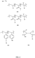
- FIG. 4 is a diagrammatic representation 400 of the molecular structures of four examples of polymer brushes 404, 408, 412, and 416, according to some embodiments of the present disclosure.
- the x, y, and z portions of polymer brushes 404 and 408 correspond to the x, y, and z portions of the first polymer brush block structure 302 illustrated in FIG. 3 .
- the R 1 groups in the x portions of polymer brushes 404 and 408 are substituents having at least one grafting group 314.
- the methyl ester group in the y portions of the polymer brushes 404 and 408 is a cleavable group 318.
- the R 2 groups in the z portions of polymer brushes 404 and 408 are acidic interface tuning groups 322, and the R 3 groups can be a hydrogen atom, a methyl group, or a trifluoromethyl group.
- the x and y portions of polymer brush 412 correspond to the x and y portions of the second polymer brush block structure 306 illustrated in FIG. 3 .
- the x portion of polymer brush 412 does not include a cleavable group 318.
- the x portion of polymer brush 412 has repeat units with R 1 grafting groups 314, and the y portion of polymer brush 412 has repeat units with phenol interface tuning groups 322.
- Polymer brush 416 is an alternating copolymer that corresponds to the third polymer brush block structure 310 illustrated in FIG. 3 .
- the carboxylic acid groups and R 3 groups on polymer brush 416 act as interface tuning groups 322.
- the R 1 group is a substituent with at least one grafting group 314, and the ester moiety is a cleavable group 318.
- FIG. 5A is a chemical reaction diagram 500 illustrating processes 500-1 and 500-2 of forming two example polymer brushes 508 and 516, according to some embodiments of the present disclosure.
- the polymer brushes 508 and 516 are formed by binding alkyne grafting groups 314 to pre-selected polymers.
- a poly(maleic anhydride) polymer 504 is a starting material for the polymer brush 508.
- This poly(maleic anhydride) polymer 504 has an R 4 group that acts as an interface tuning group on the resulting polymer brush. Examples of R 4 groups can include phenyl groups, methoxy groups, ethylene groups, etc.
- the poly(maleic anhydride) polymer 504 is combined with 4-pentyn-1-ol, which is an alcohol with a terminal alkyne moiety.
- the mixture is reacted at approximately 120 °C for approximately two hours.
- This anhydride ring-opening reaction produces a polymer brush 508 with an alkyne grafting group bound to an ester moiety.
- polyhydroxystyrene (PHOST) 512 is combined with 6-iodo-1-hexyne and potassium carbonate (K 2 CO 3 ) in an acetone solution.
- the solution is heated to produce a PHOST-derived polymer brush 516 with phenol interface tuning groups 322 on the repeat units in its x portion and alkyne grafting groups 314 on the repeat units in its y portion.
- the x and y portions of the PHOST-derived polymer brush 516 can be any length and can alternate in portions of identical length or different lengths. Adjusting the stoichiometry of this reaction can vary the number of alkyne grafting groups.
- FIG. 5B is a chemical reaction diagram illustrating a process 500-3 of grafting a polymer brush 508 to an inorganic hardmask (HM) 112, and a process 500-4 of cleaving the polymer brush 508 from the inorganic HM 112, according to some embodiments of the present disclosure.
- the polymer brush 508 is spin coated onto the inorganic HM 112, and subsequently baked for approximately 1 minute at approximately 150 °C. The baking promotes the covalent bonding of the alkyne grafting groups 314 on the polymer brush 508 to the inorganic HM 112.
- subsequent preparation steps can be carried out (e.g., photoresist application and lithographic patterning).
- the polymer brush 508 is cleaved from the inorganic HM 112.
- a combination of acid (H + ) and heat are applied to the attached polymer brush 508 in order to break the bond between the grafting group 314 and the remainder of the polymer brush 508.
- the residual polymer 504 can then be rinsed away by an organic solvent.
- the photolithographic processes involving the polymer brushes 104 disclosed herein can be used in the fabrication of integrated circuit chips for use in electronic devices.
- integrated circuit chips can be distributed by the fabricator as raw wafers, bare die, packaged in a single chip form (e.g., a plastic carrier with leads attached to a motherboard or other carrier), packaged in a multichip form (e.g., a ceramic carrier with surface interconnections and/or buried interconnections), etc.
- the chips can be integrated with other chips, circuit elements, signal processing devices, etc. Examples of end products that can contain the chip include computing devices (e.g., computer products including a display, keyboard or other input device, and processors), toys, appliances, automotive parts, etc.
- the polymer brushes 104 disclosed herein can be used for other purposes.
- the polymer brushes 104 could be used to improve adhesion between an inorganic surface and a non-photoresist polymer.
- the polymer brushes 104 could also be used to improve wettability of a surface, prevent biofouling on underwater surfaces, improve the performance of ion beam etching, etc.
- the compounds described herein can contain one or more chiral centers. These can include racemic mixtures, diastereomers, enantiomers, and mixtures containing one or more stereoisomer. Further, the disclosed compounds can encompass racemic forms of the compounds in addition to individual stereoisomers, as well as mixtures containing any of these. Temperature and time ranges indicated herein can include the temperature or time on either end of the range, or any temperature or time between these limits.
Landscapes
- General Physics & Mathematics (AREA)
- Physics & Mathematics (AREA)
- Chemical & Material Sciences (AREA)
- Engineering & Computer Science (AREA)
- Organic Chemistry (AREA)
- Structural Engineering (AREA)
- Architecture (AREA)
- Life Sciences & Earth Sciences (AREA)
- Materials Engineering (AREA)
- Wood Science & Technology (AREA)
- Polymers & Plastics (AREA)
- Medicinal Chemistry (AREA)
- Chemical Kinetics & Catalysis (AREA)
- Health & Medical Sciences (AREA)
- Exposure And Positioning Against Photoresist Photosensitive Materials (AREA)
- Materials For Photolithography (AREA)
- Exposure Of Semiconductors, Excluding Electron Or Ion Beam Exposure (AREA)
- Graft Or Block Polymers (AREA)
Claims (9)
- Polymerbürste (104) zum Vermitteln einer Grenzflächenwechselwirkung zwischen einem Fotolack (108) und einem organischen Substrat (112), Folgendes umfassend:eine Vielzahl von Wiederholungseinheiten (300);und dadurch gekennzeichnet, dass:mindestens ein Teil der Vielzahl von Wiederholungseinheiten eine oder mehrere Pfropfgruppen (314) zum Pfropfen auf das anorganische Substrat aufweist, wobei die eine oder die mehreren Pfropfgruppen aus einer Gruppe ausgewählt sind bestehend aus Alkynen, Acrylsäuren, Alkenen, Phosphonsäuren, Propargylen, Phosphonsäureestern und Alkoxysilanen, auf einer Identität des anorganischen Substrats basierend;wobei mindestens ein Teil der Vielzahl von Wiederholungseinheiten eine oder mehrere spaltbare Gruppen (318) aufweist;
undwobei mindestens ein Teil der Vielzahl von Wiederholungseinheiten eine oder mehrere Grenzflächeneinstellgruppen (322) zum Wechselwirken mit dem Fotolack aufweist, wobei die eine oder die mehreren Grenzflächeneinstellgruppen aus einer Gruppe ausgewählt sind bestehend aus einer sauren Gruppe und einer Ethylengruppe, auf einer Identität des Fotolacks basierend. - Verfahren für lithographisches Bemustern, Folgendes umfassend:Bereitstellen eines anorganischen Substrats (112);Absetzen (204) einer Polymerbürste (104) auf das anorganische Substrat, wobei die Polymerbürste Folgendes umfasst:eine Vielzahl von Wiederholungseinheiten (300);und dadurch gekennzeichnet, dass:mindestens ein Teil der Vielzahl von Wiederholungseinheiten eine oder mehrere Pfropfgruppen aufweist, wobei die eine oder die mehreren Pfropfgruppen aus einer Gruppe ausgewählt sind bestehend aus Alkynen, primären Hydroxylen, sekundären Hydroxylen, Acrylsäuren, Epoxiden, Alkenen, Phosphonsäuren, Propargylen, Phosphonsäureestern, Aminen, Carbonsäuren und Alkoxysilanen, auf einer Identität des anorganischen Substrats basierend;wobei mindestens ein Teil der Vielzahl von Wiederholungseinheiten eine oder mehrere spaltbare Gruppen (318) aufweist;und mindestens ein Teil der Vielzahl von Wiederholungseinheiten eine oder mehrere Grenzflächeneinstellgruppen aufweist, wobei die eine oder die mehreren Grenzflächeneinstellgruppen aus einer Gruppe ausgewählt sind bestehend aus einer sauren Gruppe, einer Phenylgruppe, einer Methoxygruppe, einer Ethylengruppe, einem Wasserstoffatom, einer Methylgruppe und einer Trifluormethylgruppe, auf einer Identität eines Fotolacks basierend;Absetzen (212) des Fotolacks auf die Polymerbürste;Maskieren (216) des Fotolacks mit einer Fotomaske, die ein Muster aufweist;Aufbringen von Energie (216) aus einer Energiequelle auf den maskierten Fotolack;Entwickeln (216) des Fotolacks, um eine Ätzmaske bilden, die das Muster aufweist; undÄtzen von Teilen (216) des anorganischen Substrats, das durch die Ätzmaske bloßgelegt ist.
- Verfahren nach Anspruch 2, wobei die Energiequelle ein lasergesteuertes Zinnplasma ist.
- Verfahren nach Anspruch 2, wobei die Energie extremes Ultraviolettlicht ist.
- Verfahren nach einem der Ansprüche 2 bis 4, wobei der Fotolack ein acrylischer Fotolack ist.
- Verfahren nach einem der Ansprüche 2 bis 4, wobei der Fotolack ein hybrider Fotolack ist.
- Verfahren nach einem der Ansprüche 2 bis 4, wobei der Fotolack ein phenolischer Fotolack ist.
- Verfahren nach einem der Ansprüche 2 bis 7, wobei das anorganische Substrat eine ultradünne anorganische Hartmaske ist.
- Verfahren zum Herstellen von integrierten Schaltungschips zur Verwendung in elektronischen Vorrichtungen durch Bereitstellen mindestens eines integrierten Schaltungschips, der in einem lithographischen Extremultraviolett-Bemusterungsverfahren (200) hergestellt wird, wobei das lithographische Extremultraviolett-Bemusterungsverfahren Folgendes umfasst:Bereitstellen eines anorganischen Substrats (112);Absetzen einer Polymerbürste (104) nach Anspruch 1 auf das anorganische Substrat.
Applications Claiming Priority (2)
| Application Number | Priority Date | Filing Date | Title |
|---|---|---|---|
| US15/686,045 US10345702B2 (en) | 2017-08-24 | 2017-08-24 | Polymer brushes for extreme ultraviolet photolithography |
| PCT/IB2018/056023 WO2019038625A1 (en) | 2017-08-24 | 2018-08-10 | POLYMER BRUSHES FOR EXTREME ULTRAVIOLET PHOTOLITHOGRAPHY |
Publications (3)
| Publication Number | Publication Date |
|---|---|
| EP3672996A1 EP3672996A1 (de) | 2020-07-01 |
| EP3672996A4 EP3672996A4 (de) | 2020-09-09 |
| EP3672996B1 true EP3672996B1 (de) | 2024-05-15 |
Family
ID=65435111
Family Applications (1)
| Application Number | Title | Priority Date | Filing Date |
|---|---|---|---|
| EP18848259.0A Active EP3672996B1 (de) | 2017-08-24 | 2018-08-10 | Polymerbürsten für extrem-ultraviolett-photolithographie |
Country Status (5)
| Country | Link |
|---|---|
| US (2) | US10345702B2 (de) |
| EP (1) | EP3672996B1 (de) |
| JP (1) | JP7712044B2 (de) |
| CN (1) | CN110997734A (de) |
| WO (1) | WO2019038625A1 (de) |
Families Citing this family (7)
| Publication number | Priority date | Publication date | Assignee | Title |
|---|---|---|---|---|
| US10345702B2 (en) | 2017-08-24 | 2019-07-09 | International Business Machines Corporation | Polymer brushes for extreme ultraviolet photolithography |
| US10831102B2 (en) * | 2018-03-05 | 2020-11-10 | International Business Machines Corporation | Photoactive polymer brush materials and EUV patterning using the same |
| US11226561B2 (en) * | 2018-08-11 | 2022-01-18 | International Business Machines Corporation | Self-priming resist for generic inorganic hardmasks |
| US11199778B2 (en) * | 2019-03-12 | 2021-12-14 | International Business Machines Corporation | Polymer brush adhesion promoter with UV cleavable linker |
| US11133195B2 (en) | 2019-04-30 | 2021-09-28 | International Business Machines Corporation | Inverse tone pillar printing method using polymer brush grafts |
| US11307496B2 (en) * | 2019-11-19 | 2022-04-19 | International Business Machines Corporation | Metal brush layer for EUV patterning |
| US20250110408A1 (en) * | 2023-09-29 | 2025-04-03 | Intel Corporation | Switchable underlayers for euv lithography |
Family Cites Families (33)
| Publication number | Priority date | Publication date | Assignee | Title |
|---|---|---|---|---|
| US20020106199A1 (en) * | 1998-05-27 | 2002-08-08 | Osamu Ikeda | Image signal recording/reproduction apparatus, method employed therein, and image signal recording apparatus |
| US6103456A (en) | 1998-07-22 | 2000-08-15 | Siemens Aktiengesellschaft | Prevention of photoresist poisoning from dielectric antireflective coating in semiconductor fabrication |
| US6423465B1 (en) * | 2000-01-28 | 2002-07-23 | International Business Machines Corporation | Process for preparing a patterned continuous polymeric brush on a substrate surface |
| DE10138105A1 (de) * | 2001-08-03 | 2003-02-27 | Infineon Technologies Ag | Fotolack und Verfahren zum Strukturieren eines solchen Fotolacks |
| US6764949B2 (en) | 2002-07-31 | 2004-07-20 | Advanced Micro Devices, Inc. | Method for reducing pattern deformation and photoresist poisoning in semiconductor device fabrication |
| US7115534B2 (en) | 2003-05-19 | 2006-10-03 | Applied Materials, Inc. | Dielectric materials to prevent photoresist poisoning |
| US7268432B2 (en) | 2003-10-10 | 2007-09-11 | International Business Machines Corporation | Interconnect structures with engineered dielectrics with nanocolumnar porosity |
| US8088352B2 (en) * | 2006-11-28 | 2012-01-03 | Vanderbilt University | Graphitic-carbon-nanofiber/polymer brushes as gas sensors |
| US7696492B2 (en) | 2006-12-13 | 2010-04-13 | Asml Netherlands B.V. | Radiation system and lithographic apparatus |
| US8294139B2 (en) | 2007-06-21 | 2012-10-23 | Micron Technology, Inc. | Multilayer antireflection coatings, structures and devices including the same and methods of making the same |
| JP2008112192A (ja) | 2008-01-21 | 2008-05-15 | Toshiba Corp | パターン形成方法および半導体装置の製造方法 |
| US8143571B1 (en) | 2008-06-03 | 2012-03-27 | Southern Illinois University | Method for fractioning peptides and other compounds |
| WO2010035799A1 (ja) | 2008-09-26 | 2010-04-01 | 国立大学法人東京医科歯科大学 | 高分子ブラシ複合体およびその製造方法 |
| US8093177B2 (en) | 2008-11-06 | 2012-01-10 | Wisconsin Alumni Research Foundation | Metal oxides having molecular and/or biomolecular functionalization |
| US8821978B2 (en) * | 2009-12-18 | 2014-09-02 | International Business Machines Corporation | Methods of directed self-assembly and layered structures formed therefrom |
| WO2011098169A1 (en) | 2010-02-09 | 2011-08-18 | Asml Netherlands B.V. | Radiation source, lithographic apparatus and device manufacturing method |
| JP5820676B2 (ja) * | 2010-10-04 | 2015-11-24 | ローム アンド ハース エレクトロニック マテリアルズ エルエルシーRohm and Haas Electronic Materials LLC | 下層組成物および下層を像形成する方法 |
| JP6035017B2 (ja) | 2010-10-04 | 2016-11-30 | ローム アンド ハース エレクトロニック マテリアルズ エルエルシーRohm and Haas Electronic Materials LLC | 下層組成物および下層を像形成する方法 |
| JP5266294B2 (ja) | 2010-11-01 | 2013-08-21 | 信越化学工業株式会社 | レジスト下層膜材料及びこれを用いたパターン形成方法 |
| US8124485B1 (en) | 2011-02-23 | 2012-02-28 | International Business Machines Corporation | Molecular spacer layer for semiconductor oxide surface and high-K dielectric stack |
| WO2012129162A2 (en) * | 2011-03-18 | 2012-09-27 | Cornell University | Methods of making patterned structures of materials, patterned structures of materials, and methods of using same |
| JP5753943B2 (ja) | 2011-05-09 | 2015-07-22 | ザ・スウォッチ・グループ・リサーチ・アンド・ディベロップメント・リミテッド | 油相溶性ポリマーブラシによる潤滑 |
| CN102983065B (zh) | 2011-09-06 | 2015-12-16 | 中芯国际集成电路制造(北京)有限公司 | 图案、掩模图案形成方法和半导体器件制造方法 |
| US8728714B2 (en) | 2011-11-17 | 2014-05-20 | Micron Technology, Inc. | Methods for adhering materials, for enhancing adhesion between materials, and for patterning materials, and related semiconductor device structures |
| JP5859420B2 (ja) | 2012-01-04 | 2016-02-10 | 信越化学工業株式会社 | レジスト下層膜材料、レジスト下層膜材料の製造方法、及び前記レジスト下層膜材料を用いたパターン形成方法 |
| US8846295B2 (en) * | 2012-04-27 | 2014-09-30 | International Business Machines Corporation | Photoresist composition containing a protected hydroxyl group for negative development and pattern forming method using thereof |
| JP6106990B2 (ja) | 2012-08-27 | 2017-04-05 | 富士通株式会社 | リソグラフィ用リンス剤、レジストパターンの形成方法、及び半導体装置の製造方法 |
| US9171720B2 (en) | 2013-01-19 | 2015-10-27 | Rohm And Haas Electronic Materials Llc | Hardmask surface treatment |
| US9773953B2 (en) | 2013-04-01 | 2017-09-26 | Rensselaer Polytechnic Institute | Organic phosphor-functionalized nanoparticles and compositions comprising the same |
| JP6240560B2 (ja) | 2013-06-26 | 2017-11-29 | 本田技研工業株式会社 | マトリックス材 |
| CN106661231A (zh) * | 2014-04-24 | 2017-05-10 | 伦斯勒理工学院 | 无基质的聚合物纳米复合物及其相关产品和方法 |
| US20170345643A1 (en) * | 2014-12-24 | 2017-11-30 | Intel Corporation | Photodefinable alignment layer for chemical assisted patterning |
| US10345702B2 (en) | 2017-08-24 | 2019-07-09 | International Business Machines Corporation | Polymer brushes for extreme ultraviolet photolithography |
-
2017
- 2017-08-24 US US15/686,045 patent/US10345702B2/en active Active
-
2018
- 2018-08-10 JP JP2020509065A patent/JP7712044B2/ja active Active
- 2018-08-10 CN CN201880054272.6A patent/CN110997734A/zh active Pending
- 2018-08-10 EP EP18848259.0A patent/EP3672996B1/de active Active
- 2018-08-10 WO PCT/IB2018/056023 patent/WO2019038625A1/en not_active Ceased
-
2019
- 2019-05-30 US US16/426,951 patent/US10656523B2/en active Active
Also Published As
| Publication number | Publication date |
|---|---|
| EP3672996A4 (de) | 2020-09-09 |
| US20190064667A1 (en) | 2019-02-28 |
| JP7712044B2 (ja) | 2025-07-23 |
| US10656523B2 (en) | 2020-05-19 |
| WO2019038625A1 (en) | 2019-02-28 |
| CN110997734A (zh) | 2020-04-10 |
| US20190285985A1 (en) | 2019-09-19 |
| JP2020531630A (ja) | 2020-11-05 |
| US10345702B2 (en) | 2019-07-09 |
| EP3672996A1 (de) | 2020-07-01 |
Similar Documents
| Publication | Publication Date | Title |
|---|---|---|
| US10656523B2 (en) | Polymer brushes for extreme ultraviolet photolithography | |
| CN102667623B (zh) | 定向自组装方法以及由此形成的分层结构 | |
| JP6342993B2 (ja) | ポリマー型熱酸発生剤を含む組成物及びそれの方法 | |
| US8877430B2 (en) | Methods of producing structures using a developer-soluble layer with multilayer technology | |
| CN102656111B (zh) | 采用193nm沉浸式光刻的定向自组装方法以及由此形成的分层结构 | |
| JP6788668B2 (ja) | ブロックコポリマーの自己組織化のための組成物及び方法 | |
| US9171720B2 (en) | Hardmask surface treatment | |
| TWI531865B (zh) | A multilayer photoresist process pattern forming method and an inorganic film forming composition for a multilayer photoresist process | |
| JP5545429B2 (ja) | 光硬化膜形成組成物及び光硬化膜形成方法 | |
| US20080213697A1 (en) | Underlayer compositions containing heterocyclic aromatic structures | |
| JP7402166B2 (ja) | 光活性ポリマーブラシ材料およびそれを使用するeuvパターニング | |
| KR20170033265A (ko) | 할로겐화설포닐알킬기를 가지는 실리콘 함유 레지스트 하층막 형성 조성물 | |
| KR20170009813A (ko) | 블록이소시아네이트 구조를 포함하는 폴리머를 포함하는 리소그래피용 레지스트 하층막 형성 조성물 | |
| CN104395328B (zh) | 具有砜结构及胺结构的含硅抗蚀剂下层膜形成组合物 | |
| EP3523823B1 (de) | Chemisch strukturierte führungsschichten zur verwendung in der chemoepitaktischen ausrichtung von block-copolymeren | |
| CN118742855A (zh) | 包含自交联性聚合物的光固化性树脂组合物 | |
| JP7189217B2 (ja) | アルカリ可溶性樹脂および架橋剤を含んでなるネガ型リフトオフレジスト組成物、並びに基板上に金属膜パターンを製造する方法 | |
| JP2021506996A (ja) | エチニル誘導体コンポジット、それを含んでなる組成物、それによる塗膜の製造方法、およびその塗膜を含んでなる素子の製造方法 | |
| KR20180053309A (ko) | 비닐기 또는 (메트)아크릴옥시기함유 폴리실록산을 포함하는 레지스트패턴 도포용 조성물 | |
| JP6776565B2 (ja) | 親撥材を用いたパターン形成方法 | |
| TWI884964B (zh) | 包含具有硬化性官能基之化合物之階差基板被覆組成物 | |
| CN121454866A (zh) | 负性感光树脂组合物、微结构、制备方法及应用 | |
| CN122072438A (zh) | 用于制造电子装置的底层组合物 | |
| JP2023101149A (ja) | レジスト下層膜形成用組成物、レジストパターン形成方法、レジスト下層膜パターンの形成方法、及びパターン形成方法 | |
| KR20240144176A (ko) | 보호막 형성용 조성물 |
Legal Events
| Date | Code | Title | Description |
|---|---|---|---|
| STAA | Information on the status of an ep patent application or granted ep patent |
Free format text: STATUS: THE INTERNATIONAL PUBLICATION HAS BEEN MADE |
|
| PUAI | Public reference made under article 153(3) epc to a published international application that has entered the european phase |
Free format text: ORIGINAL CODE: 0009012 |
|
| STAA | Information on the status of an ep patent application or granted ep patent |
Free format text: STATUS: REQUEST FOR EXAMINATION WAS MADE |
|
| 17P | Request for examination filed |
Effective date: 20200313 |
|
| AK | Designated contracting states |
Kind code of ref document: A1 Designated state(s): AL AT BE BG CH CY CZ DE DK EE ES FI FR GB GR HR HU IE IS IT LI LT LU LV MC MK MT NL NO PL PT RO RS SE SI SK SM TR |
|
| AX | Request for extension of the european patent |
Extension state: BA ME |
|
| A4 | Supplementary search report drawn up and despatched |
Effective date: 20200806 |
|
| RIC1 | Information provided on ipc code assigned before grant |
Ipc: C08L 83/00 20060101ALI20200731BHEP Ipc: C09D 201/02 20060101ALI20200731BHEP Ipc: C08F 4/00 20060101AFI20200731BHEP Ipc: G03F 7/11 20060101ALI20200731BHEP Ipc: C08G 83/00 20060101ALI20200731BHEP |
|
| RIN1 | Information on inventor provided before grant (corrected) |
Inventor name: GOLDFARB, DARIO Inventor name: VORA, ANKIT Inventor name: GLODDE, MARTIN |
|
| DAV | Request for validation of the european patent (deleted) | ||
| DAX | Request for extension of the european patent (deleted) | ||
| RAP1 | Party data changed (applicant data changed or rights of an application transferred) |
Owner name: SAMSUNG ELECTRONICS CO., LTD. |
|
| STAA | Information on the status of an ep patent application or granted ep patent |
Free format text: STATUS: EXAMINATION IS IN PROGRESS |
|
| P01 | Opt-out of the competence of the unified patent court (upc) registered |
Effective date: 20230520 |
|
| GRAP | Despatch of communication of intention to grant a patent |
Free format text: ORIGINAL CODE: EPIDOSNIGR1 |
|
| STAA | Information on the status of an ep patent application or granted ep patent |
Free format text: STATUS: GRANT OF PATENT IS INTENDED |
|
| 17Q | First examination report despatched |
Effective date: 20230621 |
|
| INTG | Intention to grant announced |
Effective date: 20230717 |
|
| GRAJ | Information related to disapproval of communication of intention to grant by the applicant or resumption of examination proceedings by the epo deleted |
Free format text: ORIGINAL CODE: EPIDOSDIGR1 |
|
| STAA | Information on the status of an ep patent application or granted ep patent |
Free format text: STATUS: EXAMINATION IS IN PROGRESS |
|
| GRAP | Despatch of communication of intention to grant a patent |
Free format text: ORIGINAL CODE: EPIDOSNIGR1 |
|
| STAA | Information on the status of an ep patent application or granted ep patent |
Free format text: STATUS: GRANT OF PATENT IS INTENDED |
|
| INTC | Intention to grant announced (deleted) | ||
| INTG | Intention to grant announced |
Effective date: 20231222 |
|
| GRAS | Grant fee paid |
Free format text: ORIGINAL CODE: EPIDOSNIGR3 |
|
| GRAA | (expected) grant |
Free format text: ORIGINAL CODE: 0009210 |
|
| STAA | Information on the status of an ep patent application or granted ep patent |
Free format text: STATUS: THE PATENT HAS BEEN GRANTED |
|
| AK | Designated contracting states |
Kind code of ref document: B1 Designated state(s): AL AT BE BG CH CY CZ DE DK EE ES FI FR GB GR HR HU IE IS IT LI LT LU LV MC MK MT NL NO PL PT RO RS SE SI SK SM TR |
|
| REG | Reference to a national code |
Ref country code: CH Ref legal event code: EP |
|
| REG | Reference to a national code |
Ref country code: DE Ref legal event code: R096 Ref document number: 602018069617 Country of ref document: DE |
|
| REG | Reference to a national code |
Ref country code: IE Ref legal event code: FG4D |
|
| REG | Reference to a national code |
Ref country code: NL Ref legal event code: FP |
|
| REG | Reference to a national code |
Ref country code: LT Ref legal event code: MG9D |
|
| PG25 | Lapsed in a contracting state [announced via postgrant information from national office to epo] |
Ref country code: IS Free format text: LAPSE BECAUSE OF FAILURE TO SUBMIT A TRANSLATION OF THE DESCRIPTION OR TO PAY THE FEE WITHIN THE PRESCRIBED TIME-LIMIT Effective date: 20240915 |
|
| PG25 | Lapsed in a contracting state [announced via postgrant information from national office to epo] |
Ref country code: BG Free format text: LAPSE BECAUSE OF FAILURE TO SUBMIT A TRANSLATION OF THE DESCRIPTION OR TO PAY THE FEE WITHIN THE PRESCRIBED TIME-LIMIT Effective date: 20240515 |
|
| PG25 | Lapsed in a contracting state [announced via postgrant information from national office to epo] |
Ref country code: HR Free format text: LAPSE BECAUSE OF FAILURE TO SUBMIT A TRANSLATION OF THE DESCRIPTION OR TO PAY THE FEE WITHIN THE PRESCRIBED TIME-LIMIT Effective date: 20240515 Ref country code: FI Free format text: LAPSE BECAUSE OF FAILURE TO SUBMIT A TRANSLATION OF THE DESCRIPTION OR TO PAY THE FEE WITHIN THE PRESCRIBED TIME-LIMIT Effective date: 20240515 |
|
| PG25 | Lapsed in a contracting state [announced via postgrant information from national office to epo] |
Ref country code: GR Free format text: LAPSE BECAUSE OF FAILURE TO SUBMIT A TRANSLATION OF THE DESCRIPTION OR TO PAY THE FEE WITHIN THE PRESCRIBED TIME-LIMIT Effective date: 20240816 |
|
| PG25 | Lapsed in a contracting state [announced via postgrant information from national office to epo] |
Ref country code: PT Free format text: LAPSE BECAUSE OF FAILURE TO SUBMIT A TRANSLATION OF THE DESCRIPTION OR TO PAY THE FEE WITHIN THE PRESCRIBED TIME-LIMIT Effective date: 20240916 |
|
| REG | Reference to a national code |
Ref country code: AT Ref legal event code: MK05 Ref document number: 1686868 Country of ref document: AT Kind code of ref document: T Effective date: 20240515 |
|
| PG25 | Lapsed in a contracting state [announced via postgrant information from national office to epo] |
Ref country code: ES Free format text: LAPSE BECAUSE OF FAILURE TO SUBMIT A TRANSLATION OF THE DESCRIPTION OR TO PAY THE FEE WITHIN THE PRESCRIBED TIME-LIMIT Effective date: 20240515 |
|
| PG25 | Lapsed in a contracting state [announced via postgrant information from national office to epo] |
Ref country code: AT Free format text: LAPSE BECAUSE OF FAILURE TO SUBMIT A TRANSLATION OF THE DESCRIPTION OR TO PAY THE FEE WITHIN THE PRESCRIBED TIME-LIMIT Effective date: 20240515 |
|
| PG25 | Lapsed in a contracting state [announced via postgrant information from national office to epo] |
Ref country code: PL Free format text: LAPSE BECAUSE OF FAILURE TO SUBMIT A TRANSLATION OF THE DESCRIPTION OR TO PAY THE FEE WITHIN THE PRESCRIBED TIME-LIMIT Effective date: 20240515 |
|
| PG25 | Lapsed in a contracting state [announced via postgrant information from national office to epo] |
Ref country code: LV Free format text: LAPSE BECAUSE OF FAILURE TO SUBMIT A TRANSLATION OF THE DESCRIPTION OR TO PAY THE FEE WITHIN THE PRESCRIBED TIME-LIMIT Effective date: 20240515 |
|
| PG25 | Lapsed in a contracting state [announced via postgrant information from national office to epo] |
Ref country code: PT Free format text: LAPSE BECAUSE OF FAILURE TO SUBMIT A TRANSLATION OF THE DESCRIPTION OR TO PAY THE FEE WITHIN THE PRESCRIBED TIME-LIMIT Effective date: 20240916 Ref country code: PL Free format text: LAPSE BECAUSE OF FAILURE TO SUBMIT A TRANSLATION OF THE DESCRIPTION OR TO PAY THE FEE WITHIN THE PRESCRIBED TIME-LIMIT Effective date: 20240515 Ref country code: NO Free format text: LAPSE BECAUSE OF FAILURE TO SUBMIT A TRANSLATION OF THE DESCRIPTION OR TO PAY THE FEE WITHIN THE PRESCRIBED TIME-LIMIT Effective date: 20240815 Ref country code: LV Free format text: LAPSE BECAUSE OF FAILURE TO SUBMIT A TRANSLATION OF THE DESCRIPTION OR TO PAY THE FEE WITHIN THE PRESCRIBED TIME-LIMIT Effective date: 20240515 Ref country code: IS Free format text: LAPSE BECAUSE OF FAILURE TO SUBMIT A TRANSLATION OF THE DESCRIPTION OR TO PAY THE FEE WITHIN THE PRESCRIBED TIME-LIMIT Effective date: 20240915 Ref country code: HR Free format text: LAPSE BECAUSE OF FAILURE TO SUBMIT A TRANSLATION OF THE DESCRIPTION OR TO PAY THE FEE WITHIN THE PRESCRIBED TIME-LIMIT Effective date: 20240515 Ref country code: GR Free format text: LAPSE BECAUSE OF FAILURE TO SUBMIT A TRANSLATION OF THE DESCRIPTION OR TO PAY THE FEE WITHIN THE PRESCRIBED TIME-LIMIT Effective date: 20240816 Ref country code: FI Free format text: LAPSE BECAUSE OF FAILURE TO SUBMIT A TRANSLATION OF THE DESCRIPTION OR TO PAY THE FEE WITHIN THE PRESCRIBED TIME-LIMIT Effective date: 20240515 Ref country code: ES Free format text: LAPSE BECAUSE OF FAILURE TO SUBMIT A TRANSLATION OF THE DESCRIPTION OR TO PAY THE FEE WITHIN THE PRESCRIBED TIME-LIMIT Effective date: 20240515 Ref country code: BG Free format text: LAPSE BECAUSE OF FAILURE TO SUBMIT A TRANSLATION OF THE DESCRIPTION OR TO PAY THE FEE WITHIN THE PRESCRIBED TIME-LIMIT Effective date: 20240515 Ref country code: AT Free format text: LAPSE BECAUSE OF FAILURE TO SUBMIT A TRANSLATION OF THE DESCRIPTION OR TO PAY THE FEE WITHIN THE PRESCRIBED TIME-LIMIT Effective date: 20240515 Ref country code: RS Free format text: LAPSE BECAUSE OF FAILURE TO SUBMIT A TRANSLATION OF THE DESCRIPTION OR TO PAY THE FEE WITHIN THE PRESCRIBED TIME-LIMIT Effective date: 20240815 |
|
| PG25 | Lapsed in a contracting state [announced via postgrant information from national office to epo] |
Ref country code: DK Free format text: LAPSE BECAUSE OF FAILURE TO SUBMIT A TRANSLATION OF THE DESCRIPTION OR TO PAY THE FEE WITHIN THE PRESCRIBED TIME-LIMIT Effective date: 20240515 |
|
| PG25 | Lapsed in a contracting state [announced via postgrant information from national office to epo] |
Ref country code: EE Free format text: LAPSE BECAUSE OF FAILURE TO SUBMIT A TRANSLATION OF THE DESCRIPTION OR TO PAY THE FEE WITHIN THE PRESCRIBED TIME-LIMIT Effective date: 20240515 |
|
| PG25 | Lapsed in a contracting state [announced via postgrant information from national office to epo] |
Ref country code: CZ Free format text: LAPSE BECAUSE OF FAILURE TO SUBMIT A TRANSLATION OF THE DESCRIPTION OR TO PAY THE FEE WITHIN THE PRESCRIBED TIME-LIMIT Effective date: 20240515 |
|
| PG25 | Lapsed in a contracting state [announced via postgrant information from national office to epo] |
Ref country code: SK Free format text: LAPSE BECAUSE OF FAILURE TO SUBMIT A TRANSLATION OF THE DESCRIPTION OR TO PAY THE FEE WITHIN THE PRESCRIBED TIME-LIMIT Effective date: 20240515 Ref country code: RO Free format text: LAPSE BECAUSE OF FAILURE TO SUBMIT A TRANSLATION OF THE DESCRIPTION OR TO PAY THE FEE WITHIN THE PRESCRIBED TIME-LIMIT Effective date: 20240515 |
|
| PG25 | Lapsed in a contracting state [announced via postgrant information from national office to epo] |
Ref country code: SM Free format text: LAPSE BECAUSE OF FAILURE TO SUBMIT A TRANSLATION OF THE DESCRIPTION OR TO PAY THE FEE WITHIN THE PRESCRIBED TIME-LIMIT Effective date: 20240515 |
|
| PG25 | Lapsed in a contracting state [announced via postgrant information from national office to epo] |
Ref country code: SM Free format text: LAPSE BECAUSE OF FAILURE TO SUBMIT A TRANSLATION OF THE DESCRIPTION OR TO PAY THE FEE WITHIN THE PRESCRIBED TIME-LIMIT Effective date: 20240515 Ref country code: SK Free format text: LAPSE BECAUSE OF FAILURE TO SUBMIT A TRANSLATION OF THE DESCRIPTION OR TO PAY THE FEE WITHIN THE PRESCRIBED TIME-LIMIT Effective date: 20240515 Ref country code: RO Free format text: LAPSE BECAUSE OF FAILURE TO SUBMIT A TRANSLATION OF THE DESCRIPTION OR TO PAY THE FEE WITHIN THE PRESCRIBED TIME-LIMIT Effective date: 20240515 Ref country code: EE Free format text: LAPSE BECAUSE OF FAILURE TO SUBMIT A TRANSLATION OF THE DESCRIPTION OR TO PAY THE FEE WITHIN THE PRESCRIBED TIME-LIMIT Effective date: 20240515 Ref country code: DK Free format text: LAPSE BECAUSE OF FAILURE TO SUBMIT A TRANSLATION OF THE DESCRIPTION OR TO PAY THE FEE WITHIN THE PRESCRIBED TIME-LIMIT Effective date: 20240515 Ref country code: CZ Free format text: LAPSE BECAUSE OF FAILURE TO SUBMIT A TRANSLATION OF THE DESCRIPTION OR TO PAY THE FEE WITHIN THE PRESCRIBED TIME-LIMIT Effective date: 20240515 |
|
| PG25 | Lapsed in a contracting state [announced via postgrant information from national office to epo] |
Ref country code: IT Free format text: LAPSE BECAUSE OF FAILURE TO SUBMIT A TRANSLATION OF THE DESCRIPTION OR TO PAY THE FEE WITHIN THE PRESCRIBED TIME-LIMIT Effective date: 20240515 |
|
| REG | Reference to a national code |
Ref country code: DE Ref legal event code: R097 Ref document number: 602018069617 Country of ref document: DE |
|
| PLBE | No opposition filed within time limit |
Free format text: ORIGINAL CODE: 0009261 |
|
| STAA | Information on the status of an ep patent application or granted ep patent |
Free format text: STATUS: NO OPPOSITION FILED WITHIN TIME LIMIT |
|
| REG | Reference to a national code |
Ref country code: CH Ref legal event code: PL |
|
| PG25 | Lapsed in a contracting state [announced via postgrant information from national office to epo] |
Ref country code: LU Free format text: LAPSE BECAUSE OF NON-PAYMENT OF DUE FEES Effective date: 20240810 |
|
| 26N | No opposition filed |
Effective date: 20250218 |
|
| PG25 | Lapsed in a contracting state [announced via postgrant information from national office to epo] |
Ref country code: SI Free format text: LAPSE BECAUSE OF FAILURE TO SUBMIT A TRANSLATION OF THE DESCRIPTION OR TO PAY THE FEE WITHIN THE PRESCRIBED TIME-LIMIT Effective date: 20240515 Ref country code: CH Free format text: LAPSE BECAUSE OF NON-PAYMENT OF DUE FEES Effective date: 20240831 Ref country code: MC Free format text: LAPSE BECAUSE OF FAILURE TO SUBMIT A TRANSLATION OF THE DESCRIPTION OR TO PAY THE FEE WITHIN THE PRESCRIBED TIME-LIMIT Effective date: 20240515 |
|
| REG | Reference to a national code |
Ref country code: BE Ref legal event code: MM Effective date: 20240831 |
|
| PGFP | Annual fee paid to national office [announced via postgrant information from national office to epo] |
Ref country code: GB Payment date: 20250626 Year of fee payment: 8 |
|
| PG25 | Lapsed in a contracting state [announced via postgrant information from national office to epo] |
Ref country code: BE Free format text: LAPSE BECAUSE OF NON-PAYMENT OF DUE FEES Effective date: 20240831 |
|
| PGFP | Annual fee paid to national office [announced via postgrant information from national office to epo] |
Ref country code: NL Payment date: 20250627 Year of fee payment: 8 |
|
| PG25 | Lapsed in a contracting state [announced via postgrant information from national office to epo] |
Ref country code: FR Free format text: LAPSE BECAUSE OF NON-PAYMENT OF DUE FEES Effective date: 20240831 |
|
| PG25 | Lapsed in a contracting state [announced via postgrant information from national office to epo] |
Ref country code: IE Free format text: LAPSE BECAUSE OF NON-PAYMENT OF DUE FEES Effective date: 20240810 |
|
| PG25 | Lapsed in a contracting state [announced via postgrant information from national office to epo] |
Ref country code: SE Free format text: LAPSE BECAUSE OF FAILURE TO SUBMIT A TRANSLATION OF THE DESCRIPTION OR TO PAY THE FEE WITHIN THE PRESCRIBED TIME-LIMIT Effective date: 20240515 |
|
| PGFP | Annual fee paid to national office [announced via postgrant information from national office to epo] |
Ref country code: DE Payment date: 20250624 Year of fee payment: 8 |
|
| PG25 | Lapsed in a contracting state [announced via postgrant information from national office to epo] |
Ref country code: CY Free format text: LAPSE BECAUSE OF FAILURE TO SUBMIT A TRANSLATION OF THE DESCRIPTION OR TO PAY THE FEE WITHIN THE PRESCRIBED TIME-LIMIT; INVALID AB INITIO Effective date: 20180810 |
|
| PG25 | Lapsed in a contracting state [announced via postgrant information from national office to epo] |
Ref country code: HU Free format text: LAPSE BECAUSE OF FAILURE TO SUBMIT A TRANSLATION OF THE DESCRIPTION OR TO PAY THE FEE WITHIN THE PRESCRIBED TIME-LIMIT; INVALID AB INITIO Effective date: 20180810 |