EP3674743A1 - Ansteuervorrichtung, ansteuerverfahren und lichtemittierende vorrichtung - Google Patents
Ansteuervorrichtung, ansteuerverfahren und lichtemittierende vorrichtung Download PDFInfo
- Publication number
- EP3674743A1 EP3674743A1 EP18848327.5A EP18848327A EP3674743A1 EP 3674743 A1 EP3674743 A1 EP 3674743A1 EP 18848327 A EP18848327 A EP 18848327A EP 3674743 A1 EP3674743 A1 EP 3674743A1
- Authority
- EP
- European Patent Office
- Prior art keywords
- light
- current
- output
- driving
- emitting element
- Prior art date
- Legal status (The legal status is an assumption and is not a legal conclusion. Google has not performed a legal analysis and makes no representation as to the accuracy of the status listed.)
- Granted
Links
Images


Classifications
-
- G—PHYSICS
- G01—MEASURING; TESTING
- G01S—RADIO DIRECTION-FINDING; RADIO NAVIGATION; DETERMINING DISTANCE OR VELOCITY BY USE OF RADIO WAVES; LOCATING OR PRESENCE-DETECTING BY USE OF THE REFLECTION OR RERADIATION OF RADIO WAVES; ANALOGOUS ARRANGEMENTS USING OTHER WAVES
- G01S7/00—Details of systems according to groups G01S13/00, G01S15/00, G01S17/00
- G01S7/48—Details of systems according to groups G01S13/00, G01S15/00, G01S17/00 of systems according to group G01S17/00
- G01S7/483—Details of pulse systems
- G01S7/484—Transmitters
-
- H—ELECTRICITY
- H01—ELECTRIC ELEMENTS
- H01S—DEVICES USING THE PROCESS OF LIGHT AMPLIFICATION BY STIMULATED EMISSION OF RADIATION [LASER] TO AMPLIFY OR GENERATE LIGHT; DEVICES USING STIMULATED EMISSION OF ELECTROMAGNETIC RADIATION IN WAVE RANGES OTHER THAN OPTICAL
- H01S5/00—Semiconductor lasers
- H01S5/06—Arrangements for controlling the laser output parameters, e.g. by operating on the active medium
- H01S5/068—Stabilisation of laser output parameters
- H01S5/06804—Stabilisation of laser output parameters by monitoring an external parameter, e.g. temperature
-
- G—PHYSICS
- G01—MEASURING; TESTING
- G01S—RADIO DIRECTION-FINDING; RADIO NAVIGATION; DETERMINING DISTANCE OR VELOCITY BY USE OF RADIO WAVES; LOCATING OR PRESENCE-DETECTING BY USE OF THE REFLECTION OR RERADIATION OF RADIO WAVES; ANALOGOUS ARRANGEMENTS USING OTHER WAVES
- G01S17/00—Systems using the reflection or reradiation of electromagnetic waves other than radio waves, e.g. lidar systems
- G01S17/02—Systems using the reflection of electromagnetic waves other than radio waves
- G01S17/06—Systems determining position data of a target
- G01S17/08—Systems determining position data of a target for measuring distance only
-
- G—PHYSICS
- G01—MEASURING; TESTING
- G01S—RADIO DIRECTION-FINDING; RADIO NAVIGATION; DETERMINING DISTANCE OR VELOCITY BY USE OF RADIO WAVES; LOCATING OR PRESENCE-DETECTING BY USE OF THE REFLECTION OR RERADIATION OF RADIO WAVES; ANALOGOUS ARRANGEMENTS USING OTHER WAVES
- G01S17/00—Systems using the reflection or reradiation of electromagnetic waves other than radio waves, e.g. lidar systems
- G01S17/88—Lidar systems specially adapted for specific applications
- G01S17/89—Lidar systems specially adapted for specific applications for mapping or imaging
-
- G—PHYSICS
- G01—MEASURING; TESTING
- G01S—RADIO DIRECTION-FINDING; RADIO NAVIGATION; DETERMINING DISTANCE OR VELOCITY BY USE OF RADIO WAVES; LOCATING OR PRESENCE-DETECTING BY USE OF THE REFLECTION OR RERADIATION OF RADIO WAVES; ANALOGOUS ARRANGEMENTS USING OTHER WAVES
- G01S17/00—Systems using the reflection or reradiation of electromagnetic waves other than radio waves, e.g. lidar systems
- G01S17/88—Lidar systems specially adapted for specific applications
- G01S17/93—Lidar systems specially adapted for specific applications for anti-collision purposes
-
- G—PHYSICS
- G01—MEASURING; TESTING
- G01S—RADIO DIRECTION-FINDING; RADIO NAVIGATION; DETERMINING DISTANCE OR VELOCITY BY USE OF RADIO WAVES; LOCATING OR PRESENCE-DETECTING BY USE OF THE REFLECTION OR RERADIATION OF RADIO WAVES; ANALOGOUS ARRANGEMENTS USING OTHER WAVES
- G01S7/00—Details of systems according to groups G01S13/00, G01S15/00, G01S17/00
- G01S7/48—Details of systems according to groups G01S13/00, G01S15/00, G01S17/00 of systems according to group G01S17/00
- G01S7/481—Constructional features, e.g. arrangements of optical elements
- G01S7/4816—Constructional features, e.g. arrangements of optical elements of receivers alone
-
- G—PHYSICS
- G01—MEASURING; TESTING
- G01S—RADIO DIRECTION-FINDING; RADIO NAVIGATION; DETERMINING DISTANCE OR VELOCITY BY USE OF RADIO WAVES; LOCATING OR PRESENCE-DETECTING BY USE OF THE REFLECTION OR RERADIATION OF RADIO WAVES; ANALOGOUS ARRANGEMENTS USING OTHER WAVES
- G01S7/00—Details of systems according to groups G01S13/00, G01S15/00, G01S17/00
- G01S7/48—Details of systems according to groups G01S13/00, G01S15/00, G01S17/00 of systems according to group G01S17/00
- G01S7/483—Details of pulse systems
- G01S7/486—Receivers
- G01S7/4865—Time delay measurement, e.g. time-of-flight measurement, time of arrival measurement or determining the exact position of a peak
-
- G—PHYSICS
- G01—MEASURING; TESTING
- G01S—RADIO DIRECTION-FINDING; RADIO NAVIGATION; DETERMINING DISTANCE OR VELOCITY BY USE OF RADIO WAVES; LOCATING OR PRESENCE-DETECTING BY USE OF THE REFLECTION OR RERADIATION OF RADIO WAVES; ANALOGOUS ARRANGEMENTS USING OTHER WAVES
- G01S7/00—Details of systems according to groups G01S13/00, G01S15/00, G01S17/00
- G01S7/48—Details of systems according to groups G01S13/00, G01S15/00, G01S17/00 of systems according to group G01S17/00
- G01S7/497—Means for monitoring or calibrating
-
- H—ELECTRICITY
- H01—ELECTRIC ELEMENTS
- H01S—DEVICES USING THE PROCESS OF LIGHT AMPLIFICATION BY STIMULATED EMISSION OF RADIATION [LASER] TO AMPLIFY OR GENERATE LIGHT; DEVICES USING STIMULATED EMISSION OF ELECTROMAGNETIC RADIATION IN WAVE RANGES OTHER THAN OPTICAL
- H01S5/00—Semiconductor lasers
- H01S5/02—Structural details or components not essential to laser action
- H01S5/022—Mountings; Housings
- H01S5/0225—Out-coupling of light
- H01S5/02257—Out-coupling of light using windows, e.g. specially adapted for back-reflecting light to a detector inside the housing
-
- H—ELECTRICITY
- H01—ELECTRIC ELEMENTS
- H01S—DEVICES USING THE PROCESS OF LIGHT AMPLIFICATION BY STIMULATED EMISSION OF RADIATION [LASER] TO AMPLIFY OR GENERATE LIGHT; DEVICES USING STIMULATED EMISSION OF ELECTROMAGNETIC RADIATION IN WAVE RANGES OTHER THAN OPTICAL
- H01S5/00—Semiconductor lasers
- H01S5/06—Arrangements for controlling the laser output parameters, e.g. by operating on the active medium
- H01S5/062—Arrangements for controlling the laser output parameters, e.g. by operating on the active medium by varying the potential of the electrodes
- H01S5/0625—Arrangements for controlling the laser output parameters, e.g. by operating on the active medium by varying the potential of the electrodes in multi-section lasers
-
- H—ELECTRICITY
- H01—ELECTRIC ELEMENTS
- H01S—DEVICES USING THE PROCESS OF LIGHT AMPLIFICATION BY STIMULATED EMISSION OF RADIATION [LASER] TO AMPLIFY OR GENERATE LIGHT; DEVICES USING STIMULATED EMISSION OF ELECTROMAGNETIC RADIATION IN WAVE RANGES OTHER THAN OPTICAL
- H01S5/00—Semiconductor lasers
- H01S5/06—Arrangements for controlling the laser output parameters, e.g. by operating on the active medium
- H01S5/068—Stabilisation of laser output parameters
- H01S5/06825—Protecting the laser, e.g. during switch-on/off, detection of malfunctioning or degradation
-
- H—ELECTRICITY
- H03—ELECTRONIC CIRCUITRY
- H03K—PULSE TECHNIQUE
- H03K17/00—Electronic switching or gating, i.e. not by contact-making and –breaking
- H03K17/51—Electronic switching or gating, i.e. not by contact-making and –breaking characterised by the components used
- H03K17/78—Electronic switching or gating, i.e. not by contact-making and –breaking characterised by the components used using opto-electronic devices, i.e. light-emitting and photoelectric devices electrically- or optically-coupled
-
- H—ELECTRICITY
- H10—SEMICONDUCTOR DEVICES; ELECTRIC SOLID-STATE DEVICES NOT OTHERWISE PROVIDED FOR
- H10F—INORGANIC SEMICONDUCTOR DEVICES SENSITIVE TO INFRARED RADIATION, LIGHT, ELECTROMAGNETIC RADIATION OF SHORTER WAVELENGTH OR CORPUSCULAR RADIATION
- H10F30/00—Individual radiation-sensitive semiconductor devices in which radiation controls the flow of current through the devices, e.g. photodetectors
- H10F30/20—Individual radiation-sensitive semiconductor devices in which radiation controls the flow of current through the devices, e.g. photodetectors the devices having potential barriers, e.g. phototransistors
-
- H—ELECTRICITY
- H10—SEMICONDUCTOR DEVICES; ELECTRIC SOLID-STATE DEVICES NOT OTHERWISE PROVIDED FOR
- H10F—INORGANIC SEMICONDUCTOR DEVICES SENSITIVE TO INFRARED RADIATION, LIGHT, ELECTROMAGNETIC RADIATION OF SHORTER WAVELENGTH OR CORPUSCULAR RADIATION
- H10F77/00—Constructional details of devices covered by this subclass
- H10F77/40—Optical elements or arrangements
-
- G—PHYSICS
- G01—MEASURING; TESTING
- G01S—RADIO DIRECTION-FINDING; RADIO NAVIGATION; DETERMINING DISTANCE OR VELOCITY BY USE OF RADIO WAVES; LOCATING OR PRESENCE-DETECTING BY USE OF THE REFLECTION OR RERADIATION OF RADIO WAVES; ANALOGOUS ARRANGEMENTS USING OTHER WAVES
- G01S17/00—Systems using the reflection or reradiation of electromagnetic waves other than radio waves, e.g. lidar systems
- G01S17/02—Systems using the reflection of electromagnetic waves other than radio waves
- G01S17/06—Systems determining position data of a target
- G01S17/08—Systems determining position data of a target for measuring distance only
- G01S17/10—Systems determining position data of a target for measuring distance only using transmission of interrupted, pulse-modulated waves
- G01S17/14—Systems determining position data of a target for measuring distance only using transmission of interrupted, pulse-modulated waves wherein a voltage or current pulse is initiated and terminated in accordance with the pulse transmission and echo reception respectively, e.g. using counters
-
- G—PHYSICS
- G01—MEASURING; TESTING
- G01S—RADIO DIRECTION-FINDING; RADIO NAVIGATION; DETERMINING DISTANCE OR VELOCITY BY USE OF RADIO WAVES; LOCATING OR PRESENCE-DETECTING BY USE OF THE REFLECTION OR RERADIATION OF RADIO WAVES; ANALOGOUS ARRANGEMENTS USING OTHER WAVES
- G01S17/00—Systems using the reflection or reradiation of electromagnetic waves other than radio waves, e.g. lidar systems
- G01S17/88—Lidar systems specially adapted for specific applications
- G01S17/89—Lidar systems specially adapted for specific applications for mapping or imaging
- G01S17/894—Three-dimensional [3D] imaging with simultaneous measurement of time-of-flight at a two-dimensional [2D] array of receiver pixels, e.g. time-of-flight cameras or flash lidar
-
- G—PHYSICS
- G01—MEASURING; TESTING
- G01S—RADIO DIRECTION-FINDING; RADIO NAVIGATION; DETERMINING DISTANCE OR VELOCITY BY USE OF RADIO WAVES; LOCATING OR PRESENCE-DETECTING BY USE OF THE REFLECTION OR RERADIATION OF RADIO WAVES; ANALOGOUS ARRANGEMENTS USING OTHER WAVES
- G01S7/00—Details of systems according to groups G01S13/00, G01S15/00, G01S17/00
- G01S7/48—Details of systems according to groups G01S13/00, G01S15/00, G01S17/00 of systems according to group G01S17/00
- G01S7/483—Details of pulse systems
- G01S7/486—Receivers
- G01S7/4868—Controlling received signal intensity or exposure of sensor
-
- H—ELECTRICITY
- H01—ELECTRIC ELEMENTS
- H01S—DEVICES USING THE PROCESS OF LIGHT AMPLIFICATION BY STIMULATED EMISSION OF RADIATION [LASER] TO AMPLIFY OR GENERATE LIGHT; DEVICES USING STIMULATED EMISSION OF ELECTROMAGNETIC RADIATION IN WAVE RANGES OTHER THAN OPTICAL
- H01S5/00—Semiconductor lasers
- H01S5/02—Structural details or components not essential to laser action
- H01S5/022—Mountings; Housings
- H01S5/02208—Mountings; Housings characterised by the shape of the housings
-
- H—ELECTRICITY
- H01—ELECTRIC ELEMENTS
- H01S—DEVICES USING THE PROCESS OF LIGHT AMPLIFICATION BY STIMULATED EMISSION OF RADIATION [LASER] TO AMPLIFY OR GENERATE LIGHT; DEVICES USING STIMULATED EMISSION OF ELECTROMAGNETIC RADIATION IN WAVE RANGES OTHER THAN OPTICAL
- H01S5/00—Semiconductor lasers
- H01S5/02—Structural details or components not essential to laser action
- H01S5/022—Mountings; Housings
- H01S5/023—Mount members, e.g. sub-mount members
- H01S5/02325—Mechanically integrated components on mount members or optical micro-benches
-
- H—ELECTRICITY
- H01—ELECTRIC ELEMENTS
- H01S—DEVICES USING THE PROCESS OF LIGHT AMPLIFICATION BY STIMULATED EMISSION OF RADIATION [LASER] TO AMPLIFY OR GENERATE LIGHT; DEVICES USING STIMULATED EMISSION OF ELECTROMAGNETIC RADIATION IN WAVE RANGES OTHER THAN OPTICAL
- H01S5/00—Semiconductor lasers
- H01S5/02—Structural details or components not essential to laser action
- H01S5/022—Mountings; Housings
- H01S5/0233—Mounting configuration of laser chips
- H01S5/02345—Wire-bonding
-
- H—ELECTRICITY
- H01—ELECTRIC ELEMENTS
- H01S—DEVICES USING THE PROCESS OF LIGHT AMPLIFICATION BY STIMULATED EMISSION OF RADIATION [LASER] TO AMPLIFY OR GENERATE LIGHT; DEVICES USING STIMULATED EMISSION OF ELECTROMAGNETIC RADIATION IN WAVE RANGES OTHER THAN OPTICAL
- H01S5/00—Semiconductor lasers
- H01S5/04—Processes or apparatus for excitation, e.g. pumping, e.g. by electron beams
- H01S5/042—Electrical excitation ; Circuits therefor
- H01S5/0428—Electrical excitation ; Circuits therefor for applying pulses to the laser
-
- H—ELECTRICITY
- H01—ELECTRIC ELEMENTS
- H01S—DEVICES USING THE PROCESS OF LIGHT AMPLIFICATION BY STIMULATED EMISSION OF RADIATION [LASER] TO AMPLIFY OR GENERATE LIGHT; DEVICES USING STIMULATED EMISSION OF ELECTROMAGNETIC RADIATION IN WAVE RANGES OTHER THAN OPTICAL
- H01S5/00—Semiconductor lasers
- H01S5/06—Arrangements for controlling the laser output parameters, e.g. by operating on the active medium
- H01S5/062—Arrangements for controlling the laser output parameters, e.g. by operating on the active medium by varying the potential of the electrodes
- H01S5/06209—Arrangements for controlling the laser output parameters, e.g. by operating on the active medium by varying the potential of the electrodes in single-section lasers
- H01S5/06216—Pulse modulation or generation
-
- H—ELECTRICITY
- H01—ELECTRIC ELEMENTS
- H01S—DEVICES USING THE PROCESS OF LIGHT AMPLIFICATION BY STIMULATED EMISSION OF RADIATION [LASER] TO AMPLIFY OR GENERATE LIGHT; DEVICES USING STIMULATED EMISSION OF ELECTROMAGNETIC RADIATION IN WAVE RANGES OTHER THAN OPTICAL
- H01S5/00—Semiconductor lasers
- H01S5/06—Arrangements for controlling the laser output parameters, e.g. by operating on the active medium
- H01S5/068—Stabilisation of laser output parameters
- H01S5/0683—Stabilisation of laser output parameters by monitoring the optical output parameters
- H01S5/06835—Stabilising during pulse modulation or generation
Definitions
- the present technology relates to a driving device, a driving method, and a light-emitting unit, and particularly to a driving device, a driving method, and a light-emitting unit that make it possible to appropriately drive a light-emitting element.
- a relational expression between a bias current of a laser diode (LD) and light-receiving power be found on the basis of two types of bias currents having different near-threshold current values and light-receiving power detected by a light-receiving element in a case where the LD is caused to emit light by the two types of bias currents. Furthermore, it has been proposed that a current value when the light-receiving power is zero in the found relational expression be calculated as a threshold current of the LD (for example, see PTL 1).
- PTL 1 does not take into consideration the influence of background light, such as light from the outside.
- an LD is installed inside a chassis, and thus there exists little background light around the LD.
- an LD is installed in a position that allows laser light to be outputted to the outside, and thus there exists background light around the LD. Accordingly, even when the LD does not yet emit light, light-receiving power detected by a light-receiving element does not become zero. Therefore, in a case where a threshold current of the LD is calculated by means of the invention of PTL 1, the influence of background light causes an error in a calculation result. Then, because of this error, there is a possibility that the LD may not be driven appropriately.
- the present technology has been made in view of such circumstances, and is intended to make it possible to appropriately drive a light-emitting element such as an LD.
- a driving device includes: a setting section that sets at least one of a bias current of a light-emitting element or a target current for setting output light from the light-emitting element to desired intensity on the basis of a result of detection of an offset light amount when the light-emitting element does not emit light, the detection being performed by a light-receiving element that receives a portion of the output light; and an output controller that controls an output of a driving current of the light-emitting element on the basis of at least one of the set bias current or the set target current.
- a driving method implemented by a driving device includes: setting at least one of a bias current of a light-emitting element or a target current for setting output light from the light-emitting element to desired intensity on the basis of a result of detection of an offset light amount when the light-emitting element does not emit light, the detection being performed by a light-receiving element that receives a portion of the output light; and controlling an output of a driving current of the light-emitting element on the basis of at least one of the set bias current or the set target current.
- a light-emitting unit includes: a light-emitting element; a light-receiving element that receives a portion of output light from the light-emitting element; a setting section that sets at least one of a bias current of the light-emitting element or a target current for setting the output light to desired intensity on the basis of a result of detection of an offset light amount when the light-emitting element does not emit light, the detection being performed by the light-receiving element; and an output controller that controls an output of a driving current of the light-emitting element on the basis of at least one of the set bias current or the set target current.
- At least one of the bias current of the light-emitting element or the target current for setting the output light to desired intensity is set on the basis of the result of detection of the offset light amount when the light-emitting element does not emit light.
- the detection is performed by the light-receiving element that receives a portion of the output light from the light-emitting element.
- the output of the driving current of the light-emitting element is controlled on the basis of at least one of the set bias current or the set target current.
- the first or second aspect of the present technology it is possible to appropriately set at least one of the bias current of the light-emitting element or the target current. Furthermore, according to the first or second aspect of the present technology, it is possible to appropriately drive the light-emitting element.
- FIG. 1 illustrates an embodiment of a ranging module to which the present technology is applied.
- a ranging module 100 is a module that measures a distance to an object using laser light by a ToF method.
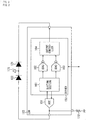
- the ranging module 100 includes a substrate 111, an optical module 112, a laser diode driver (LDD) 113, a lens 114, a range image sensor 115, and an LSI 116.
- the optical module 112, the LDD 113, the lens 114, the range image sensor 115, and the LSI 116 are mounted on the substrate 111. Furthermore, the optical module 112 and the LDD 113 form a light emitter 101 that performs emission of laser light.
- the optical module 112 includes a laser diode (LD) 121, a photodiode (PD) 122, and a diffuser 123.
- LD laser diode
- PD photodiode
- the LD 121 is a light-emitting element that outputs laser light of a predetermined wavelength. For example, under control of the LDD 113, the LD 121 outputs laser light to be used for measurement of a distance to an object.
- the PD 122 is a light-receiving element used for measurement of the intensity (power) of laser light outputted from the LD 121, and outputs a received light signal indicating an amount of received light.
- the PD 122 receives return light that is a portion of the laser light outputted from the LD 121 and returning by being reflected by the diffuser 123, and outputs a received light signal indicating an amount of the return light.
- the diffuser 123 is a diffusing member provided for the purpose of making laser light outputted from the LD 121 meet a safety standard, such as IEC (International Electrotechnical Commission) 60825-1.
- the laser light outputted from the LD 121 passes through the diffuser 123 thereby being diffused, and becomes diffused light. Furthermore, a portion of the laser light is reflected by the diffuser 123, and its return light enters the PD 122.
- the LDD 113 supplies a driving current to the LD 121, thereby controlling light emission of the LD 121. Furthermore, the LDD 113 performs auto power control (APC) to control the intensity (power) of laser light outputted from the LD 121 on the basis of a received light signal from the PD 122.
- APC auto power control
- the lens 114 When laser light is applied from the LD 121 to an object subjected to distance measurement, the lens 114 forms an image of reflected light reflected on and returned from the object on a light-receiving surface of the range image sensor 115.
- the range image sensor 115 is, for example, a ToF range image sensor, and detects a distance (a depth) to a subject on a pixel to pixel basis. More specifically, the range image sensor 115 detects a phase difference between laser light outputted from the LD 121 and reflected light from the subject on a pixel to pixel basis, and supplies range image data indicating the detected phase difference to the LSI 116.
- the LSI 116 controls the LDD 113 and the range image sensor 115, and performs various processing, such as detection of a distance to a subject, on the basis of range image data.
- the disposition of the optical module 112, the LDD 113, the lens 114, the range image sensor 115, and the LSI 116 on the substrate 111 illustrated in FIG. 1 is an example, and may be changed as appropriate.
- FIG. 2 illustrates a configuration example of the LDD 113 illustrated in FIG. 1 .
- the LDD 113 includes an A/D converter (ADC) 151 and a driver 152.
- the driver 152 includes a setting section 161, a current output D/A converter (IDAC) 162, an IDAC 163, and an output controller 164.
- ADC A/D converter
- IDAC current output D/A converter
- an anode of the LD 121 and a cathode of the PD 122 are coupled to a power source 171 of a predetermined voltage. That is, in this example, the LD 121 is an anode common. Furthermore, an input terminal of the ADC 151 is grounded through a resistance 172.
- the ADC 151 performs an A/D conversion of a received light signal supplied from the PD 122, and supplies a digital received light signal to the setting section 161.
- the setting section 161 performs the settings for a switching current and a bias current to be supplied to the LD 121 on the basis of a received light signal from the ADC 151 under control of the LSI 116.
- the setting section 161 supplies the IDAC 162 with a digital input signal indicating a value of a switching current to be outputted from the IDAC 162.
- the setting section 161 supplies the IDAC 163 with a digital input signal indicating a value of a bias current to be outputted from the IDAC 163.
- the IDAC 162 performs a D/A conversion of an input signal, and generates a switching current having a value indicated by the input signal, and then supplies the switching current to the output controller 164.
- the IDAC 163 performs a D/A conversion of an input signal, and generates a bias current having a value indicated by the input signal, and then supplies the bias current to the output controller 164.
- the output controller 164 controls the output of a driving current to the LD 121.
- the output controller 164 amplifies a switching current, and generates a pulsed driving current having a peak at a value in which the amplified switching current and a bias current are added up, and then supplies the driving current to the LD 121.
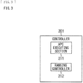
- FIG. 3 illustrates a functional configuration example of the LSI 116 illustrated in FIG. 1 .
- the LSI 116 implements functions including a controller 201.
- the controller 201 includes an APC executing section 211 and a ranging controller 212.
- the APC executing section 211 controls the LDD 113, thereby performing APC to adjust the intensity of laser light outputted from the LD 121.
- the ranging controller 212 controls the distance measurement made by the ranging module 100. More specifically, the ranging controller 212 controls the LDD 113 and the range image sensor 115, thereby controlling a process of applying laser light to an object and acquiring range image data.
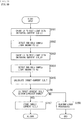
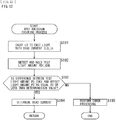
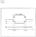
- APC execution processing performed by the ranging module 100 is described with reference to a flowchart of FIG. 4 and a timing chart of FIG. 5 . It is to be noted that this processing is performed, for example, before the distance measurement each time a distance measurement is made by the ranging module 100.
- Step S1 the ranging module 100 performs a background light measuring process.
- the background light measuring process details of the background light measuring process are described with reference to a flowchart of FIG. 6 . It is to be noted that this process is performed in a BG segment illustrated in FIG. 5 .
- the LDD 113 puts the LD 121 into a non-light-emitting state.
- the setting section 161 sets respective values of input signals to the IDAC 162 and the IDAC 163 to cause respective values of a switching current and a bias current to be zero.
- a value of a driving current supplied to the LD 121 becomes zero, and the LD 121 goes into a non-light-emitting state.
- the LDD 113 detects and holds an offset light amount PD_BG.
- the ADC 151 converts a received light signal from the PD 122 when the LD 121 is in a non-light-emitting state from analog to digital, and supplies the converted received light signal to the setting section 161.
- the setting section 161 holds a value of the received light signal at this time as an offset light amount PD_BG.
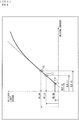
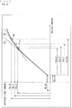
- FIG. 7 is a graph illustrating an example of light-emitting characteristics of the LD 121.
- the horizontal axis indicates a driving current of the LD 121
- the vertical axis indicates an amount of light detected by the PD 122.
- FIG. 7 illustrates a relationship between the driving current of the LD 121 and the amount of light detected by the PD 122 (the emission intensity of the LD 121).
- the LD 121 does not emit light when the driving current is less than a threshold current Ith, and emits light when the driving current becomes equal to or more than the threshold current Ith.
- the emission intensity (emission power) of the LD 121 changes substantially linearly with respect to the driving current. Therefore, the amount of light detected by the PD 122 changes substantially linearly with respect to the driving current in the linear segment.
- the emission intensity of the LD 121 changes non-linearly with respect to the driving current. Specifically, an amount of change in the emission intensity of the LD 121 with respect to the driving current becomes smaller than that in the linear segment. It is to be noted that a segment in which the driving current has exceeded the linear segment is referred to as a non-linear segment.
- the PD 122 receives ambient background light, such as light from the outside, besides return light of the laser light. Thus, the amount of light detected by the PD 122 does not become zero even when the LD 121 does not yet emit light. Therefore, the offset light amount PD_BG indicates an amount of background light detected by the PD 122.
- Step S2 the ranging module 100 performs APC1.
- APC1 details of the APC1 are described with reference to a flowchart of FIG. 8 . It is to be noted that this process is performed in an APC1 section illustrated in FIG. 5 .
- the LDD 113 causes the LD 121 to emit light with a bias current ILD_L1.
- the setting section 161 sets respective values of input signals to the IDAC 162 and the IDAC 163 to cause the value of the switching current to be zero and the value of the bias current to be ILD_L1.
- a bias current having a value of ILD_L1 (hereinafter, referred to as a bias current ILD_L1) is supplied to the LD 121, and the LD 121 emits light.
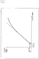
- FIG. 9 illustrates a relationship between the driving current of the LD 121 and the amount of light detected by the PD 122, as with FIG. 7 .
- the bias current ILD_L1 is set, for example, to a value that is near the threshold current Ith of the LD 121 and is larger than the threshold current Ith in the linear segment. It is to be noted that in the APC execution processing, for example, a pre-calculated design value (for example, a catalogue value) is used as the threshold current Ith.
- the LDD 113 detects and holds a sample light amount PD_L1.
- the ADC 151 converts a received light signal from the PD 122 from analog to digital, and supplies the converted received light signal to the setting section 161.
- the setting section 161 holds a value of the received light signal at this time as a sample light amount PD_L1.
- the sample light amount PD_L1 is an amount of light detected by the PD 122 when the LD 121 emits light with the bias current ILD_L1.
- the LDD 113 causes the LD 121 to emit light with a bias current ILD_H1.
- the setting section 161 sets respective values of input signals to the IDAC 162 and the IDAC 163 to cause the value of the switching current to be zero and the value of the bias current to be ILD_H1.
- a bias current having a value of ILD_H1 (hereinafter, referred to as a bias current ILD_H1) is supplied to the LD 121, and the LD 121 emits light.
- the value of the bias current ILD_H1 is set, for example, to a value that is near the threshold current Ith and is larger than the bias current ILD_L1 in the linear segment.
- a sample light amount PD_H1 is detected and held through a process similar to Step S132.
- the sample light amount PD_H1 is an amount of light detected by the PD 122 when the LD 121 emits light with the bias current ILD_H1.
- the setting section 161 calculates a bias current ILD_th.
- the bias current ILD_L1 and the bias current ILD_H1 are included in the linear segment. Accordingly, as illustrated in FIG. 9 , the setting section 161 performs a 2-point interpolation function using a point L1 corresponding to the bias current ILD_L1 and the sample light amount PD_L1 and a point H1 corresponding to the bias current ILD_H1 and the sample light amount PD_H1, thereby calculating a bias current ILD_th corresponding to the offset light amount PD_BG.
- a value of this bias current ILD th is approximately equal to the threshold current Ith, and thus the accuracy of the bias current is improved.
- the bias current ILD th may be calculated by an interpolation process using, for example, three or more sample light amounts in a case where the LD 121 is caused to emit light by three or more bias currents having different values.
- the setting section 161 determines whether or not the bias current ILD_th is within an expected range. That is, a result of the calculation of the bias current ILD_th is checked. For example, the setting section 161 compares the bias current ILD_th with the threshold current Ith, and, in a case where a difference between the two is equal to or less than a predetermined determination value, determines that the bias current ILD th is within the expected range, and the process moves on to Step S137.
- the setting section 161 stores the bias current ILD_th.
- Step S136 in a case where a difference between the bias current ILD_th and the threshold current Ith exceeds the predetermined determination value, the setting section 161 determines that the bias current ILD_th is out of the expected range, and the process moves on to Step S138.
- Step S138 the LDD 113 performs error processing.
- the setting section 161 supplies an error signal to the APC executing section 211. Furthermore, for example, under control of the APC executing section 211, the setting section 161 sets respective values of input signals to the IDAC 162 and the IDAC 163 to zero. Thus, the value of the driving current supplied to the LD 121 becomes zero, and the LD 121 goes into a non-light-emitting state.
- Step S3 the ranging module 100 performs APC2.
- APC2 details of the APC2 are described with reference to a flowchart of FIG. 10 . It is to be noted that this process is performed in an APC2 segment illustrated in FIG. 5 .
- the LDD 113 causes the LD 121 to emit light with a switching current ILD_L2.
- the setting section 161 sets respective values of input signals to the IDAC 162 and the IDAC 163 to cause the value of the switching current to be ILD_L2 and the value of the bias current to be ILD_th.
- a pulsed driving current in which a switching current having a value of ILD L2 (hereinafter, referred to as a switching current ILD L2) and the bias current ILD th are added up is supplied to the LD 121, and the LD 121 emits light.
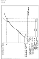
- FIG. 11 illustrates a relationship between the driving current of the LD 121 and the amount of light detected by the PD 122, as with FIG. 7 .
- the ranging module 100 needs to apply laser light to a distant object and receive its reflected light; therefore, the desired intensity (hereinafter, referred to as the target intensity) of laser light from the LD 121 used at the time of distance measurement becomes very high. Therefore, a driving current for causing laser light of the target intensity to be outputted from the LD 121 exceeds the linear segment and is included in the non-linear segment.
- the switching current ILD_L2 is set within the non-linear segment. More specifically, for example, the switching current ILD_L2 is set to a value smaller than a virtual target current ILD_T' in the non-linear segment.
- the virtual target current ILD T' here is a virtual value of a switching current for causing laser light of the target intensity to be outputted from the LD 121 (a current that the bias current ILD_th is subtracted from the driving current).
- a value of a switching current with respect to a target light amount PD_T calculated on the basis of a straight line S2 based on the assumption that also in the non-linear segment, the emission intensity of the LD 121 changes linearly with respect to the driving current is set as a virtual target current ILD_T'.
- the target light amount PD_T is an amount of light detected by the PD 122 when laser light of the target intensity is outputted from the LD 121, and is found in advance, for example, by an actual measurement or calculation.
- a sample light amount PD_L2 is detected and held through a process similar to Step S132 illustrated in FIG. 10 .
- the sample light amount PD_L2 is an amount of light detected by the PD 122 when the LD 121 emits light with a driving current in which the switching current ILD_L2 and the bias current ILD_th are added up.
- the LDD 113 causes the LD 121 to emit light with a switching current ILD_H2.
- the setting section 161 sets respective values of input signals to the IDAC 162 and the IDAC 163 to cause the value of the switching current to be ILD_H2 and the value of the bias current to be ILD_th.
- a pulsed driving current in which a switching current having a value of ILD_H2 (hereinafter, referred to as a switching current ILD_H2) and the bias current ILD th are added up is supplied to the LD 121, and the LD 121 emits light.
- the switching current ILD_H2 is set, for example to a value that is near the virtual target current ILD_T' and is larger than the virtual target current ILD T' in the non-linear segment.
- a sample light amount PD_H2 is detected and held through a process similar to Step S132 illustrated in FIG. 10 .
- the sample light amount PD_H2 is an amount of light detected by the PD 122 when the LD 121 emits light with a driving current in which the switching current ILD_H2 and the bias current ILD_th are added up.
- the setting section 161 calculates a target current ILD_T. For example, as illustrated in FIG. 11 , the setting section 161 performs a 2-point interpolation function using a point L2 corresponding to the switching current ILD L2 and the sample light amount PD_L2 and a point H2 corresponding to the switching current ILD_H2 and the sample light amount PD_H2, thereby calculating a target current ILD_T that is a switching current corresponding to the target light amount PD_T.
- the target current ILD_T is calculated on the basis of a straight line S1 connecting the point L2 and the point H2. Therefore, the accuracy of the target current is improved as compared with, for example, the virtual target current ILD T' calculated on the basis of the straight line S2 based on the assumption that the emission intensity of the LD 121 changes linearly with respect to the driving current also in the non-linear segment.
- the target current ILD_T may be calculated by an interpolation process using, for example, three or more sample light amounts in a case where the LD 121 is caused to emit light by three or more switching currents having different values.
- the setting section 161 determines whether or not the target current ILD_T is within an expected range. That is, a result of the calculation of the target current ILD_T is checked. For example, the setting section 161 compares the target current ILD_T with the virtual target current ILD T', and, in a case where a difference between the two is equal to or less than a predetermined determination value, determines that the target current ILD_T is within the expected range, and the process moves on to Step S167.
- the setting section 161 stores the target current ILD_T.
- Step S166 in a case where a difference between the target current ILD_T and the virtual target current ILD_T' exceeds the predetermined determination value, the setting section 161 determines that the target current ILD_T is out of the expected range, and the process moves on to Step S168.
- Step S168 error processing is performed as with the process at Step S138 illustrated in FIG. 8 .
- Step S4 the ranging module 100 performs an APC1 emission checking process.
- the APC1 emission checking process details of the APC1 emission checking process are described with reference to a flowchart of FIG. 12 . It is to be noted that this process is performed in an APC1 emission checking segment illustrated in FIG. 5 .
- the LDD 113 causes the LD 121 to emit light with a bias current ILD_th.
- the setting section 161 sets respective values of input signals to the IDAC 162 and the IDAC 163 to cause the value of the switching current to be zero and the value of the bias current to be ILD_th.
- a bias current having a value of ILD th (hereinafter, referred to as a bias current ILD_th) is supplied to the LD 121, and the LD 121 emits light.
- Step S192 a test light amount PD1_CHK is detected and held through a process similar to Step S132 illustrated in FIG. 10 .
- FIG. 13 illustrates a relationship between the driving current of the LD 121 and the amount of light detected by the PD 122, as with FIG. 7 .
- the test light amount PD1_CHK is an amount of light detected by the PD 122 when the LD 121 emits light with the bias current ILD_th.
- the setting section 161 determines whether or not a difference between the test light amount PD1_CHK and the offset light amount PD BG is equal to or less than a determination value. Through this determination process, the accuracy of the bias current ILD_th set by the APC1 is checked. For example, in a case where it has been determined that a difference between the two is equal to or less than the predetermined determination value, i.e., in a case where the accuracy of the bias current ILD_th is high, the process moves on to Step S194.
- the setting section 161 determines a bias current. That is, the setting section 161 determines the bias current ILD th set by the APC1 to be a bias current of the LD 121.
- Step S193 in a case where it has been determined that a difference between the two exceeds the predetermined determination value, i.e., in a case where the accuracy of the bias current ILD_th is low, the process moves on to Step S195.
- Step S195 error processing is performed as with the process at Step S138 illustrated in FIG. 8 .
- Step S5 the ranging module 100 performs an APC2 emission checking process.
- the APC2 emission checking process details of the APC2 emission checking process are described with reference to a flowchart of FIG. 14 . It is to be noted that this process is performed in an APC2 emission checking section illustrated in FIG. 5 .
- the LDD 113 causes the LD 121 to emit light with a target current ILD_T.
- the setting section 161 sets respective values of input signals to the IDAC 162 and the IDAC 163 to cause the value of the switching current to be ILD_T and the value of the bias current to be ILD_th.
- a pulsed driving current in which a switching current having a value of ILD T (the target current ILD T) and the bias current ILD_th are added up is supplied to the LD 121, and the LD 121 emits light.
- Step S222 a test light amount PD2_CHK is detected and held through a process similar to Step S132 illustrated in FIG. 10 .
- FIG. 15 illustrates a relationship between the driving current of the LD 121 and the amount of light detected by the PD 122, as with FIG. 7 .
- the test light amount PD2_CHK is an amount of light detected by the PD 122 when the LD 121 emits light with the driving current in which the target current ILD_T and the bias current ILD_th are added up.
- the setting section 161 determines whether or not a difference between the test light amount PD2_CHK and the offset light amount PD_BG is equal to or less than a determination value. Through this determination process, abnormality of the diffuser 123 (for example, installation failure, damage, etc. of the diffuser 123) is detected.
- test light amount PD2_CHK becomes approximately equal to an amount of light in which the return light and background light are added up.
- a difference between the test light amount PD2_CHK and the offset light amount PD_BG becomes larger and exceeds the predetermined determination value.
- the laser light outputted from the LD 121 is made into diffused light by the diffuser 123, and is reduced in intensity and then is applied to an object 301. Therefore, the laser light outputted from the optical module 112 is able to meet a predetermined safety standard.
- test light amount PD2_CHK becomes approximately equal to an amount of background light.
- the test light amount PD2_CHK and the offset light amount PD_BG are approximately equal, and thus a difference between the two is equal to or less than the predetermined determination value.
- the laser light outputted from the LD 121 is directly applied to the object 301 without being reduced in intensity. Therefore, there is a possibility that the laser light outputted from the optical module 112 may not meet the predetermined safety standard.
- Step S224 the process moves on to Step S224.
- the setting section 161 determines whether or not a difference between the test light amount PD2_CHK and the target light amount PD_T is equal to or less than a determination value. Through this determination process, the accuracy of the target current ILD_T set by the APC2 is checked. For example, in a case where it has been determined that a difference between the two is equal to or less than the predetermined determination value, i.e., in a case where the accuracy of the target current ILD_T is high, the process moves on to Step S225.
- the setting section 161 determines a target current. That is, the setting section 161 determines the target current ILD_T set by the APC2 to be a switching current of the LD 121 at the time of distance measurement.
- Step S224 in a case where it has been determined that a difference between the test light amount PD2_CHK and the target light amount PD_T exceeds the predetermined determination value, i.e., in a case where the accuracy of the target current ILD_T is low, the process moves on to Step S226.
- Step S223 in a case where it has been determined that a difference between the test light amount PD2_CHK and the offset light amount PD BG is equal to or less than the predetermined determination value, i.e., in a case where there is assumed to be abnormality of the diffuser 123, the process moves on to Step S226.
- Step S226 error processing is performed as with the process at Step S138 illustrated in FIG. 8 .
- error processing is performed as with the process at Step S138 illustrated in FIG. 8 .
- the diffuser 123 is removed, laser light that does not meet the safety standard is prevented from being applied to the human eyes, etc.
- Step S6 the ranging module 100 starts the distance measurement.
- the driving current (the bias current and the target current) of the LD 121 before the distance measurement.
- a bias current ILD_th' that is a current when the amount of light detected by the PD 122 becomes zero is calculated.
- E1 there is an error E1 between the bias current ILD th' and the threshold current Ith of the LD 121.
- a target current ILD T' (the same current as the above-described virtual target current ILD_T') with respect to the target intensity of the LD 121 is calculated.
- an error E2 there is an error E2 between the target current ILD_T' and a target current calculated in a case where the non-linear segment is taken into consideration.
- a delay in light emission of the LD 121 may occur, for example, as illustrated in FIG. 19 . That is, the timing for the LD 121 to emit light with respect to the driving current is delayed, and the pulse width of the laser light becomes narrower than the pulse width of the driving current. As a result, there is a possibility that the accuracy of the distance measurement may be reduced.
- the influence of background light and the non-linear segment of the LD 121 are taken into consideration, and the accuracy of setting the bias current and the target current of the LD 121 is improved.
- the LD 121 is appropriately driven, and the delay in light emission of the LD 121 is suppressed, and therefore the accuracy of the distance measurement is improved.
- the threshold current Ith of the LD 121 changes with temperature and aged deterioration. Meanwhile, in the ranging module 100, APC is performed before the distance measurement; therefore, the bias current and the target current are appropriately set in accordance with a change in the threshold current Ith. As a result, the LD 121 is appropriately driven, and the delay in light emission of the LD 121 is suppressed, and therefore the accuracy of the distance measurement is improved.
- the ranging module 100 is able to detect abnormality of the diffuser 123 without using a physical detection mechanism. Consequently, it is possible to easily enhance the safety of the ranging module 100.
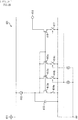
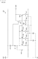
- FIG. 20 is a circuit diagram illustrating a configuration example of a switching current generating circuit 401 that is the first embodiment of the switching current generating circuit.
- the switching current generating circuit 401 includes a current mirror circuit. Specifically, the switching current generating circuit 401 includes a power source 411, a current source 412, transistors 413a to 413c each including an N-type MOSFET, switches 414a to 414c, a capacitor 415, a transistor 416 including an N-type MOSFET, a switch 417, and an output terminal 418.
- the current source 412 includes, for example, the IDAC 162 illustrated in FIG. 2 , and is coupled to between the power source 411 and drains of the transistors 413a to 413c.
- Gates of the transistors 413a to 413c and a gate of the transistor 416 are coupled to each other, and are coupled to the drains of the transistors 413a to 413c.
- a source of the transistor 413a is grounded through the switch 414a.
- the switch 414a is a dummy switch that is always ON.
- a source of the transistor 413b is grounded through the switch 414b.
- the switch 414b is turned ON or OFF by an ON signal or an OFF signal supplied from the APC executing section 211 or the ranging controller 212 illustrated in FIG. 3 . Then, when the switch 414b is turned ON, the transistor 413b is turned ON; when the switch 414b is turned OFF, the transistor 413b is turned OFF.
- a source of the transistor 413c is grounded through the switch 414c.
- the switch 414c is turned ON or OFF by an ON signal or an OFF signal supplied from the APC executing section 211 or the ranging controller 212. Then, when the switch 414c is turned ON, the transistor 413c is turned ON; when the switch 414c is turned OFF, the transistor 413c is turned OFF.
- a drain of the transistor 416 is coupled to the output terminal 418, and a source of the transistor 416 is grounded through the switch 417.
- the switch 417 is turned ON or OFF by an ON signal or an OFF signal supplied from the APC executing section 211 or the ranging controller 212. Then, when the switch 417 is turned ON, the transistor 416 is turned ON; when the switch 417 is turned OFF, the transistor 416 is turned OFF.
- One end of the capacitor 415 is coupled to the drains of the transistors 413a to 413c, and the other end of the capacitor 415 is grounded.
- the capacitor 415 is provided for suppressing variations in gate voltages of the transistors 413a to 413c and the transistor 416 (hereinafter, also referred to as a gate voltage of the current mirror circuit).
- the transistors 413a to 413c form an input stage of the current mirror circuit, and the transistor 416 forms an output stage of the current mirror circuit.
- the size ratio (specifically, (gate width)/(gate length)) of the transistor 413a, the transistor 413b, the transistor 413c, and the transistor 416 is set to Na : Nb : Nc : (Na+Nb+Nc) ⁇ M. Then, depending on whether the input-stage transistors 413a to 413c are in ON or OFF state, the current mirror ratio (also referred to as the ratio of output current and input current or the return ratio) of the current mirror circuit changes.
- the current mirror ratio is (Na+Nb+Nc) ⁇ M/Na.
- the transistor 416 is OFF, and thus no current is outputted.
- the current mirror ratio is (Na+Nb+Nc) ⁇ M/(Na+Nb). Therefore, in the intermediate state, an output current (a switching current) that is (Na+Nb+Nc) ⁇ M/(Na+Nb) times the input current supplied from the current source 402 is outputted from the output terminal 408.
- the current mirror ratio satisfies the equation, the initial state > the intermediate state > the steady state.
- the switching current generating circuit 401 controls the timing to turn the transistors 413b and 413c and the transistor 416 ON or OFF, and thereby improving the slew rate of the driving current of the LD 121.
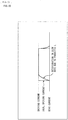
- FIG. 21 A right part of FIG. 21 illustrates an equivalent circuit of the LD 121 on the left.
- the equivalent circuit of the LD 121 is represented by an active resistance 431, a parasitic capacitance 432, a power source 433 that supplies a minimum voltage of an operating voltage Vop of the LD 121, and a parasitic inductance 434. Additionally, the active resistance 431 and the parasitic capacitance 432 are coupled in parallel to between the power source 171 and a + terminal of the power source 433, and the parasitic inductance 434 is coupled to a - terminal of the power source 433.
- the intensity of required laser light is low; therefore, the LD 121 is used in a low driving current range. Then, in the low driving current range, the slew rate at the time of rise of the driving current is determined mainly by respective time constants of the active resistance 431 and the parasitic capacitance 432.
- the LD 121 is used in a very high driving current range. Then, as the driving current becomes higher, the parasitic inductance 434 has greater influence on the slew rate at the time of rise of the driving current than the active resistance 431 and the parasitic capacitance 432.
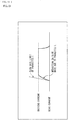
- FIG. 22 illustrates an example of respective waveforms of an ideal driving current and an actual driving current of the LD 121.
- the horizontal axis indicates a time
- the vertical axis indicates a current value.
- the waveform depicted by an alternate long and short dash line indicates the ideal driving current
- the waveform depicted by a solid line indicates the actual driving current.
- the actual driving current is more reduced in the slew rate at the time of its rise than the ideal driving current is.
- the parasitic inductance 434 puts a limit on the slew rate of the driving current, it is difficult to increase the response speed of the driving current beyond the limit.
- the driving current becomes higher, and therefore a high assist current is required.
- a differential current of a typical capacitance is used as an assist current, it is difficult to improve the slew rate because the amount of current is not enough.
- an adder circuit for supplying an assist current is required separately, which increases the size of the transistor 416. If the size of the transistor 416 is increased, a parasitic capacitance between the drain and the gate and between the gate and the source of the transistor 416 becomes larger.
- the gate voltage of the transistor 416 decreases for an instant when the transistor 416 is turned ON, and after that, gradually increases. And then, the gate voltage of the transistor 416 decreases, and thereby a drain current of the transistor 416 (an output current of the current mirror circuit) is reduced. This causes distortion like a sag in the output current of the current mirror circuit.
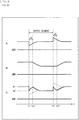
- the horizontal axis indicates a time
- the vertical axis indicates respective gate voltages of the transistors 413a to 413c and the transistor 416 (a gate voltage of the current mirror circuit).
- an output current (a switching current) of the switching current generating circuit 401 is turned ON or OFF by turning the switches 414b and 414c and the switch 417 ON or OFF at the same time.
- Part A of FIG. 24 illustrates changes in the gate voltage caused by turning the output-stage switch 417 ON or OFF, thereby turning the transistor 416 ON or OFF.
- Part B of FIG. 24 illustrates changes in the gate voltage caused by turning the input-stage switches 414b and 414c ON or OFF, thereby turning the transistors 413b and 413c ON or OFF.
- Part C of FIG. 24 illustrates an actual gate voltage in which parts A and B of FIG. 24 are added up.
- the switch 414a Before a time t1, the switch 414a is turned ON, and the switches 414b and 414c and the switch 417 are turned OFF, and thereby the transistor 413a is turned ON, and the transistors 413b and 413c and the transistor 416 are turned OFF. That is, the current mirror circuit is set in the initial state, and the current mirror ratio is set to (Na+Nb+Nc) ⁇ M/Na. However, the transistor 416 is OFF, and thus no current is outputted from the switching current generating circuit 401.
- the switches 414b and 414c and the switch 417 are turned ON, and thereby the transistors 413b and 413c and the transistor 416 are turned ON.
- the current mirror circuit makes transition from the initial state to the steady state, and the current mirror ratio decreases from (Na+Nb+Nc) ⁇ M/Na to M (the current mirror ratio is reduced). Furthermore, the output of an output current that is M times the input current from the switching current generating circuit 401 is started.
- the output-stage transistor 416 is turned ON, which causes a variation in the gate voltage due to the parasitic capacitance between the drain and the gate and between the gate and the source of the transistor 416. That is, as illustrated in part A of FIG. 24 , the gate voltage decreases for an instant at the time t1, and after that, is gradually back to the original voltage, and becomes stable.
- the input-stage transistors 413b and 413c are turned ON, and thereby, the gate voltage gradually decreases, and becomes stable at a predetermined voltage, as illustrated in part B of FIG. 24 .
- the switches 414b and 414c and the switch 417 are turned OFF, and thereby the transistors 413b and 413c and the transistor 416 are turned OFF.
- the current mirror circuit makes transition from the steady state to the initial state, and the current mirror ratio increases from M to (Na+Nb+Nc) ⁇ M/Na (the current mirror ratio is raised).
- the output of a current from the switching current generating circuit 401 is stopped. Therefore, a segment from the time t1 to the time t2 is an output segment of the output current.
- the transistor 416 is turned OFF, which causes a variation in the gate voltage due to the parasitic capacitance of the transistor 416. That is, as illustrated in part A of FIG. 24 , the gate voltage increases for an instant at the time t2, and after that, is gradually back to the original voltage, and becomes stable.
- the input-stage transistors 413b and 413c are turned OFF, and thereby the gate voltage gradually increases and becomes stable at the voltage in the initial state, as illustrated in part B of FIG. 24 .
- the size of the transistor 413a it becomes possible to offset the variation in the gate voltage caused by switching of the output stage illustrated in part A of FIG. 24 and the decrease and increase in the gate voltage caused by switching of the input stage illustrated in part B of FIG. 24 . That is, without having to add a large capacitance, a difference in the gate voltage between before and after the switching of the input-stage transistors 413b and 413c causes an electrical charge to be supplied to the parasitic capacitance of the output-stage transistor 416, and the parasitic capacitance is charged. Thus, the variation in the gate voltage at the time of switching of the transistor 416 is offset.
- the gate voltage exhibits a nearly flat characteristic. That is, in the initial state before the time t1, the transistors 413b and 413c are OFF, and thus the gate voltage becomes a voltage V1 that is higher than a voltage V2 in the steady state. At the time t1, the transistors 413b and 413c and the transistor 416 are turned ON, and the gate voltage instantaneously decreases to the voltage V2 and becomes stable with the transition from the initial state to the steady state. Furthermore, at the time t2, the transistors 413b and 413c and the transistor 416 are turned OFF, and the gate voltage instantaneously increases to the voltage V2 and becomes stable with the transition from the steady state to the initial state.
- the gate voltage changes in nearly flat pulses, and thus the output current of the switching current generating circuit 401 also changes in nearly flat pulses, and a waveform of the output current becomes stable.
- the input-stage transistors 413a to 413c are turned ON or OFF with a delay of a delay time ⁇ T [nsec] after the output-stage transistor 416 is turned ON or OFF.
- the delay time ⁇ T is variable, and is set to be, for example, within 3 nsec.
- Part A of FIG. 25 illustrates, as with part A of FIG. 24 , changes in the gate voltage caused by turning the output-stage switch 417 ON or OFF, thereby turning the transistor 416 ON or OFF.
- Part B of FIG. 25 illustrates, as with part B of FIG. 24 , changes in the gate voltage caused by turning the input-stage switches 414b and 414c ON or OFF, thereby turning the transistors 413b and 413c ON or OFF.
- Part C of FIG. 25 illustrates an actual gate voltage in which parts A and B of FIG. 25 are added up.
- the timing to turn the output-stage switch 417 and the transistor 416 ON or OFF is the same as that in an example of FIG. 24 , and thus the waveform of the gate voltage in part A of FIG. 25 is similar to the waveform of the gate voltage in part A of FIG. 24 .
- the timing to turn the input-stage switches 414b and 414c and the transistors 413b and 413c ON or OFF is delayed by the delay time AT from the timing to turn the output-stage switch 417 and the transistor 416 ON or OFF. Therefore, the waveform of the gate voltage in part B of FIG. 25 is delayed by the delay time ⁇ T from the waveform of the gate voltage in part B of FIG. 24 .
- the gate voltage becomes the voltage V1 higher than the voltage V2 before the time t1, as with an example of part C of FIG. 24 .
- the transistor 416 is turned ON, and accordingly, the gate voltage decreases for an instant and then increases.
- the delay time ⁇ T from the time t1 to a time t11 at which the transistors 413b and 413c are turned ON, there is a raised part where the gate voltage becomes higher than the voltage V2 in the steady state.
- the magnitude of the assist current is adjusted by adjusting the size ratio Na : Nb : Nc of the input-stage transistors 413a to 413c. Furthermore, time to supply the assist current is adjusted by adjusting the delay time ⁇ T Therefore, it becomes possible to suppress the influence of the parasitic inductance 434 and improve the slew rate of the driving current of the LD 121 by appropriately setting the size ratio Na : Nb : Nc and the delay time ⁇ T.
- the transistors 413b and 413c are turned ON, and accordingly the gate voltage gradually decreases and becomes stable at the voltage V2. Furthermore, the current mirror ratio decreases from (Na+Nb+Nc) ⁇ M/Na to M (the current mirror ratio is reduced). Thus, the output current of the switching current generating circuit 401 becomes a predetermined current (a target current), and becomes stable.
- the transistor 416 is turned OFF, and accordingly the gate voltage increases for an instant and then decreases. Furthermore, the output of a current from the switching current generating circuit 401 is stopped.
- the transistors 413b and 413c are turned OFF, and accordingly the gate voltage gradually increases and becomes stable at the voltage V1. Furthermore, the current mirror ratio increases from M to (Na+Nb+Nc) ⁇ M/Na (the current mirror ratio is raised).
- a variation in the gate voltage after the time t2 basically does not affect the output current because the transistor 416 is OFF. However, for example, if an interval until the transistor 416 is turned ON next is short, and this variation in the gate voltage affects the output current, it becomes possible to mask the variation in the gate voltage by adding, for example, a simple logic circuit.
- FIG. 26 illustrates a waveform of the gate voltage, as with part C of FIG. 24 and part C of FIG. 25 .
- the switch 414b and the switch 417 are turned ON, and thereby the input-stage transistor 413b and the output-stage transistor 416 are turned ON.
- the current mirror circuit makes transition from the initial state to the intermediate state, and the current mirror ratio decreases from (Na+Nb+Nc) ⁇ M/Na to (Na+Nb+Nc) ⁇ M/(Na+Nb) (the current mirror ratio is reduced).
- the output of an output current that is (Na+Nb+Nc) ⁇ M/(Na+Nb) times (> M times) the input current from the switching current generating circuit 401 is started.
- the output current becomes higher than the output current in the steady state (M times the input current) from the time t1 to the time t11, and therefore is able to be used as an assist current at the time of rise of the driving current of the LD 121.
- the magnitude of the assist current is adjusted by adjusting the size ratio Na : Nb : Nc of the input-stage transistors 413a to 413c. Furthermore, time to supply the assist current is adjusted by adjusting the delay time ⁇ T Therefore, it becomes possible to suppress the influence of the parasitic inductance 434 and improve the slew rate of the driving current of the LD 121 by appropriately setting the size ratio Na : Nb : Nc and the delay time ⁇ T.
- the switch 414c is turned ON, and thereby the input-stage transistor 413c is turned ON.
- the current mirror circuit makes transition from the intermediate state to the steady state, and the current mirror ratio changes from (Na+Nb+Nc) ⁇ M/(Na+Nb) to M (the current mirror ratio is reduced).
- the gate voltage decreases from the voltage V12 to the voltage V2, and becomes stable.
- an output current of the switching current generating circuit 401 becomes the predetermined current (the target current), and becomes stable.
- the switch 414b and the switch 417 are turned OFF, and thereby the input-stage transistor 413b and the output-stage transistor 416 are turned OFF.
- the current mirror ratio changes from M to (Na+Nb+Nc) ⁇ M/(Na+Nb) (the current mirror ratio is raised).
- the gate voltage increases from the voltage V2 to the voltage V12, and becomes stable. Furthermore, the output of a current from the switching current generating circuit 401 is stopped.
- the switch 414c is turned OFF, and thereby the input-stage transistor 413c is turned OFF.
- the current mirror ratio increases from (Na+Nb+Nc) ⁇ M/(Na+Nb) to (Na+Nb+Nc) ⁇ M/Na (the current mirror ratio is raised).
- the gate voltage instantaneously increases flat from the voltage V12 to the voltage V11, and becomes stable.
- the switching current generating circuit 401 is applicable whether control of the driving current is analog or digital,
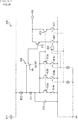
- FIG. 27 is a circuit diagram illustrating a configuration example of a switching current generating circuit 451 that is a second embodiment of the switching current generating circuit.
- the above-described switching current generating circuit 401 is effective particularly in a case where the voltage of the power source 171 ( FIG. 2 ) to which the LD 121 is coupled is sufficiently high.
- the switching current generating circuit 401 does not sometimes work well. That is, in the switching current generating circuit 401, when the driving current starts flowing into the LD 121, the drain voltage of the transistor 416 decreases due to a reverse voltage caused by the parasitic inductance 434. Then, in the case where the voltage of the power source 171 is low, there is a possibility that the drain voltage of the transistor 416 may be insufficient, and a drain current (an output current) may not be sufficiently outputted.
- the switching current generating circuit 451 illustrated in FIG. 27 takes a measure against this phenomenon.
- the switching current generating circuit 451 differs from the switching current generating circuit 401 illustrated in FIG. 20 in that the switching current generating circuit 451 further includes a variable resistance 461, a switch 462, and an AND circuit 463.
- the variable resistance 461 is very low in resistance value, and serves as a shunt circuit. Furthermore, the variable resistance 461 is coupled to the output stage of the current mirror circuit through the switch 417. More specifically, the variable resistance 461 is coupled to between the drain of the transistor 416 (the output terminal 418) and the ground through the switch 417. Then, the variable resistance 461 is coupled to and separated from the output stage of the current mirror circuit by the switch 417.
- the AND circuit 463 inputs an ON signal to the switch 462 in a case where an ON signal is inputted to the switch 414b, and an OFF signal is inputted to the switch 414c, and inputs an OFF signal to the switch 462 in other cases. Therefore, the switch 462 is turned ON in a case where the switch 414b is turned ON, and thereby the transistor 413b is turned ON, and the switch 414c is turned OFF, and thereby the transistor 413c is turned OFF, and is turned OFF in other cases.
- the switching current generating circuit 451 is in a state where the variable resistance 461 is coupled to the output stage of the current mirror circuit.
- the LD 121 is driven with a voltage applied through the variable resistance 461.
- the voltage of the power source 171 is low, it is possible to increase the slew rate of the driving current of the LD 121 without depending on the drain voltage of the transistor 416.
- the current starts flowing into the parasitic inductance 434, and, the drain voltage of the transistor 416 becomes stable.
- an ON signal is inputted to the switch 414c, and the transistor 413c is turned ON an.
- an ON signal is inputted to the switch 462, and the switch 462 is turned OFF.
- the variable resistance 461 is separated from the output stage of the current mirror circuit by the switch 417. Even if the variable resistance 461 is separated in this way, the drain voltage of the transistor 416 is stable, and therefore it is possible to stably supply the driving current to the LD 121.
- a degree of improvement in the slew rate of the driving current of the LD 121 made by the shunt circuit changes depending on the magnitude of a stationary driving current (the driving current in the steady state) after the operation of the LD 121 becomes stable. That is, the higher the stationary driving current becomes, the larger the amount of improvement the shunt circuit provides; the lower the stationary driving current becomes, the smaller the amount of improvement the shunt circuit provides. Therefore, it is desirable that the resistance value of the variable resistance 461 be decreased as the stationary driving current becomes higher, and the resistance value of the variable resistance 461 be increased as the stationary driving current becomes lower.
- the stationary driving current of the LD 121 varies with the output current (the switching current) from the switching current generating circuit 451, and the output current varies with the input current inputted from the current source 412 to the switching current generating circuit 451. Therefore, it is desirable that the resistance value of the variable resistance 461 be decreased as the input current becomes higher, and the resistance value of the variable resistance 461 be increased as the input current becomes lower. This makes it possible to keep the effect of the shunt circuit nearly uniformly and keep the slew rate of the driving current nearly uniformly regardless of the magnitude of the stationary driving current of the LD 121.
- FIG. 28 is a circuit diagram illustrating a configuration example of a switching current generating circuit 501 that is a third embodiment of the switching current generating circuit.
- the switching current generating circuit 501 differs from the switching current generating circuit 451 illustrated in FIG. 27 in that the switching current generating circuit 501 does not include the variable resistance 461, and further includes a resistance 511 and a transistor 512 including an N-type
- the resistance 511 is coupled to between the current source 412 and the drain of the transistor 413a.
- the drain of the transistor 512 is coupled to the output terminal 418, and the gate is coupled to between the current source 412 and the resistance 511, and the source is grounded through the switch 462.
- a variable resistance corresponding to the variable resistance 461 of the switching current generating circuit 451 in FIG. 27 is realized by an on-resistance of the transistor 512.
- a gate voltage of the transistor 512 is defined by a current (an input current) of the current source 412 and the resistance 511. That is, the gate voltage of the transistor 512 linearly changes with voltages generated in both ends of the resistance 511 by the input current. That is, the gate voltage of the transistor 512 increases as the input current becomes higher, and decreases as the input current becomes lower.
- FIG. 29 is a circuit diagram illustrating a configuration example of a switching current generating circuit 551 that is a fourth embodiment of the switching current generating circuit.
- the switching current generating circuit 551 differs from the switching current generating circuit 501 illustrated in FIG. 28 in that the switching current generating circuit 551 further includes a switch 561.
- the switch 561 is coupled to between the current source 412 and the resistance 511 and to the gate of the transistor 512.
- the switch 561 is turned ON when receiving an ON signal inputted from the APC executing section 211 or the ranging controller 212, and couples the gate of the transistor 512 to between the current source 412 and the resistance 511.
- the transistor 512 is turned ON, and the shunt circuit is enabled.
- the switch 561 is turned OFF when receiving an OFF signal inputted from the APC executing section 211 or the ranging controller 212, and couples the gate of the transistor 512 to the ground.
- the transistor 512 is turned OFF, and the shunt circuit is disabled.
- the switch 561 may be turned OFF to disable the shunt circuit.
- the APC2 at step S3 and the APC2 emission checking process at step S5 may be omitted in the APC execution processing illustrated in FIG. 4 , and the target current may be set as a fixed value. It is to be noted that in a case where the APC2 emission checking process is omitted, the process of detecting abnormality of the diffuser 123 may be remained.
- the background light measuring process at Step S1, the APC1 at Step S2, and the APC1 emission checking process at step S4 may be omitted in the APC execution processing illustrated in FIG. 4 , and the bias current may be set as a fixed value.
- an offset light amount may be detected without omitting the background light measuring process, and the detected offset light amount may be used for calculation of the target current.
- the output of laser light from the LD 121 may not be stopped.
- the subsequent processing may be continued using a preset bias current or target current without using the bias current or target current determined to be an error.
- the output of laser light from the LD 121 may not be stopped except in a case where abnormality of the diffuser 123 is detected.
- the subsequent processing may be continued using a preset target current without using the target current determined to be an error.
- each current mirror circuit illustrated in FIGs. 20 and 27 to 29 , there is described an example of using an N-type MOSFET as each transistor on the assumption that the LD 121 is an anode common; however, for example, in a case where the LD 121 is a cathode common, a P-type MOSFET only has to be used as each transistor. Furthermore, for example, it is also possible for each current mirror circuit to use a transistor other than a MOSFET.
- the PD 122 receives, as return light, laser light reflected by the diffuser 123; however, for example, the PD 122 may receive return light reflected by another member. Furthermore, the PD 122 may receive a portion of laser light outputted from the LD 121 by means other than return light.
- the configuration example of the ranging module 100 is not limited to the above-described example.
- the light emitter 101, the range image sensor 115, and the LSI 116 may be provided in different modules from one another, or one of the three may be provided in a different module.
- the technology according to the present disclosure is applicable to various products.
- the technology according to the present disclosure may be achieved in the form of an apparatus to be mounted to a mobile body of any kind.
- the mobile body may include an automobile, an electric vehicle, a hybrid electric vehicle, a motorcycle, a bicycle, any personal mobility device, an airplane, a drone, a vessel, and a robot.
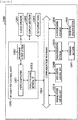
- FIG. 30 is a block diagram depicting an example of schematic configuration of a vehicle control system as an example of a mobile body control system to which the technology according to an embodiment of the present disclosure can be applied.
- the vehicle control system 12000 includes a plurality of electronic control units connected to each other via a communication network 12001.
- the vehicle control system 12000 includes a driving system control unit 12010, a body system control unit 12020, an outside-vehicle information detecting unit 12030, an in-vehicle information detecting unit 12040, and an integrated control unit 12050.
- a microcomputer 12051, a sound/image output section 12052, and a vehicle-mounted network interface (I/F) 12053 are illustrated as a functional configuration of the integrated control unit 12050.
- the driving system control unit 12010 controls the operation of devices related to the driving system of the vehicle in accordance with various kinds of programs.
- the driving system control unit 12010 functions as a control device for a driving force generating device for generating the driving force of the vehicle, such as an internal combustion engine, a driving motor, or the like, a driving force transmitting mechanism for transmitting the driving force to wheels, a steering mechanism for adjusting the steering angle of the vehicle, a braking device for generating the braking force of the vehicle, and the like.
- the body system control unit 12020 controls the operation of various kinds of devices provided to a vehicle body in accordance with various kinds of programs.
- the body system control unit 12020 functions as a control device for a keyless entry system, a smart key system, a power window device, or various kinds of lamps such as a headlamp, a backup lamp, a brake lamp, a turn signal, a fog lamp, or the like.
- radio waves transmitted from a mobile device as an alternative to a key or signals of various kinds of switches can be input to the body system control unit 12020.
- the body system control unit 12020 receives these input radio waves or signals, and controls a door lock device, the power window device, the lamps, or the like of the vehicle.
- the outside-vehicle information detecting unit 12030 detects information about the outside of the vehicle including the vehicle control system 12000.
- the outside-vehicle information detecting unit 12030 is connected with an imaging section 12031.
- the outside-vehicle information detecting unit 12030 makes the imaging section 12031 image an image of the outside of the vehicle, and receives the imaged image.
- the outside-vehicle information detecting unit 12030 may perform processing of detecting an object such as a human, a vehicle, an obstacle, a sign, a character on a road surface, or the like, or processing of detecting a distance thereto.
- the imaging section 12031 is an optical sensor that receives light, and which outputs an electric signal corresponding to a received light amount of the light.
- the imaging section 12031 can output the electric signal as an image, or can output the electric signal as information about a measured distance.
- the light received by the imaging section 12031 may be visible light, or may be invisible light such as infrared rays or the like.
- the in-vehicle information detecting unit 12040 detects information about the inside of the vehicle.
- the in-vehicle information detecting unit 12040 is, for example, connected with a driver state detecting section 12041 that detects the state of a driver.
- the driver state detecting section 12041 for example, includes a camera that images the driver.
- the in-vehicle information detecting unit 12040 may calculate a degree of fatigue of the driver or a degree of concentration of the driver, or may determine whether the driver is dozing.
- the microcomputer 12051 can calculate a control target value for the driving force generating device, the steering mechanism, or the braking device on the basis of the information about the inside or outside of the vehicle which information is obtained by the outside-vehicle information detecting unit 12030 or the in-vehicle information detecting unit 12040, and output a control command to the driving system control unit 12010.
- the microcomputer 12051 can perform cooperative control intended to implement functions of an advanced driver assistance system (ADAS) which functions include collision avoidance or shock mitigation for the vehicle, following driving based on a following distance, vehicle speed maintaining driving, a warning of collision of the vehicle, a warning of deviation of the vehicle from a lane, or the like.
- ADAS advanced driver assistance system
- the microcomputer 12051 can perform cooperative control intended for automatic driving, which makes the vehicle to travel autonomously without depending on the operation of the driver, or the like, by controlling the driving force generating device, the steering mechanism, the braking device, or the like on the basis of the information about the outside or inside of the vehicle which information is obtained by the outside-vehicle information detecting unit 12030 or the in-vehicle information detecting unit 12040.
- the microcomputer 12051 can output a control command to the body system control unit 12020 on the basis of the information about the outside of the vehicle which information is obtained by the outside-vehicle information detecting unit 12030.
- the microcomputer 12051 can perform cooperative control intended to prevent a glare by controlling the headlamp so as to change from a high beam to a low beam, for example, in accordance with the position of a preceding vehicle or an oncoming vehicle detected by the outside-vehicle information detecting unit 12030.
- the sound/image output section 12052 transmits an output signal of at least one of a sound and an image to an output device capable of visually or auditorily notifying information to an occupant of the vehicle or the outside of the vehicle.
- an audio speaker 12061, a display section 12062, and an instrument panel 12063 are illustrated as the output device.
- the display section 12062 may, for example, include at least one of an on-board display and a head-up display.
- FIG. 31 is a diagram depicting an example of the installation position of the imaging section 12031.
- the imaging section 12031 includes imaging sections 12101, 12102, 12103, 12104, and 12105.
- the imaging sections 12101, 12102, 12103, 12104, and 12105 are, for example, disposed at positions on a front nose, sideview mirrors, a rear bumper, and a back door of the vehicle 12100 as well as a position on an upper portion of a windshield within the interior of the vehicle.
- the imaging section 12101 provided to the front nose and the imaging section 12105 provided to the upper portion of the windshield within the interior of the vehicle obtain mainly an image of the front of the vehicle 12100.
- the imaging sections 12102 and 12103 provided to the sideview mirrors obtain mainly an image of the sides of the vehicle 12100.
- the imaging section 12104 provided to the rear bumper or the back door obtains mainly an image of the rear of the vehicle 12100.
- the image of the front obtained by imaging sections 12101 and 12105 is used mainly to detect a preceding vehicle, a pedestrian, an obstacle, a signal, a traffic sign, a lane, or the like.
- FIG. 31 depicts an example of photographing ranges of the imaging sections 12101 to 12104.
- An imaging range 12111 represents the imaging range of the imaging section 12101 provided to the front nose.
- Imaging ranges 12112 and 12113 respectively represent the imaging ranges of the imaging sections 12102 and 12103 provided to the sideview mirrors.
- An imaging range 12114 represents the imaging range of the imaging section 12104 provided to the rear bumper or the back door.
- a bird's-eye image of the vehicle 12100 as viewed from above is obtained by superimposing image data imaged by the imaging sections 12101 to 12104, for example.
- At least one of the imaging sections 12101 to 12104 may have a function of obtaining distance information.
- at least one of the imaging sections 12101 to 12104 may be a stereo camera constituted of a plurality of imaging elements, or may be an imaging element having pixels for phase difference detection.
- the microcomputer 12051 can determine a distance to each three-dimensional object within the imaging ranges 12111 to 12114 and a temporal change in the distance (relative speed with respect to the vehicle 12100) on the basis of the distance information obtained from the imaging sections 12101 to 12104, and thereby extract, as a preceding vehicle, a nearest three-dimensional object in particular that is present on a traveling path of the vehicle 12100 and which travels in substantially the same direction as the vehicle 12100 at a predetermined speed (for example, equal to or more than 0 km/hour). Further, the microcomputer 12051 can set a following distance to be maintained in front of a preceding vehicle in advance, and perform automatic brake control (including following stop control), automatic acceleration control (including following start control), or the like. It is thus possible to perform cooperative control intended for automatic driving that makes the vehicle travel autonomously without depending on the operation of the driver or the like.
- automatic brake control including following stop control
- automatic acceleration control including following start control
- the microcomputer 12051 can classify three-dimensional object data on three-dimensional objects into three-dimensional object data of a two-wheeled vehicle, a standard-sized vehicle, a large-sized vehicle, a pedestrian, a utility pole, and other three-dimensional objects on the basis of the distance information obtained from the imaging sections 12101 to 12104, extract the classified three-dimensional object data, and use the extracted three-dimensional object data for automatic avoidance of an obstacle.
- the microcomputer 12051 identifies obstacles around the vehicle 12100 as obstacles that the driver of the vehicle 12100 can recognize visually and obstacles that are difficult for the driver of the vehicle 12100 to recognize visually. Then, the microcomputer 12051 determines a collision risk indicating a risk of collision with each obstacle.
- the microcomputer 12051 In a situation in which the collision risk is equal to or higher than a set value and there is thus a possibility of collision, the microcomputer 12051 outputs a warning to the driver via the audio speaker 12061 or the display section 12062, and performs forced deceleration or avoidance steering via the driving system control unit 12010. The microcomputer 12051 can thereby assist in driving to avoid collision.
- At least one of the imaging sections 12101 to 12104 may be an infrared camera that detects infrared rays.
- the microcomputer 12051 can, for example, recognize a pedestrian by determining whether or not there is a pedestrian in imaged images of the imaging sections 12101 to 12104. Such recognition of a pedestrian is, for example, performed by a procedure of extracting characteristic points in the imaged images of the imaging sections 12101 to 12104 as infrared cameras and a procedure of determining whether or not it is the pedestrian by performing pattern matching processing on a series of characteristic points representing the contour of the object.
- the sound/image output section 12052 controls the display section 12062 so that a square contour line for emphasis is displayed so as to be superimposed on the recognized pedestrian.
- the sound/image output section 12052 may also control the display section 12062 so that an icon or the like representing the pedestrian is displayed at a desired position.
- the technology according to the disclosure is applicable to, for example, the imaging sections 12101 to 12104, etc., in the configuration described above.
- the ranging module 100 of FIG. 1 is applicable. This makes it possible to improve the accuracy of detection of a distance to an object around the vehicle.
- the above-described series of processing may be performed by hardware, or may be performed by software.
- a program included in the software is installed in a computer.
- the computer here includes a computer built in dedicated hardware (for example, such as the LSI 116 illustrated in FIG. 1 ) and, for example, a general-purpose personal computer or the like that is able to implement various functions by installing various programs therein.
- the program executed by the computer may be a program to cause the processing to be performed in chronological order in line with the order described in the present specification, or may be a program to cause the processing to be performed in parallel or at required timing such as when a call has been made.
- a system means an aggregation of multiple components (devices, modules (parts), etc.), regardless of whether or not all the components are in the same chassis. Therefore, multiple devices that are housed in separate chassis and are connected through a network and one device including multiple modules housed in one chassis are both a system.
- embodiments of the present technology are not limited to the foregoing embodiments, and may be modified in a variety of ways without departing from the scope of the present technology.
- the present technology may have a configuration of cloud computing that allows multiple devices to share one function through a network and perform processing in cooperation.
- one step includes multiple processes
- the multiple processes included in the one step may be performed by one device, or may be shared and performed by multiple devices.
- the present technology may have the following configurations.
Landscapes
- Physics & Mathematics (AREA)
- Engineering & Computer Science (AREA)
- General Physics & Mathematics (AREA)
- Remote Sensing (AREA)
- Computer Networks & Wireless Communication (AREA)
- Radar, Positioning & Navigation (AREA)
- Electromagnetism (AREA)
- Condensed Matter Physics & Semiconductors (AREA)
- Optics & Photonics (AREA)
- Semiconductor Lasers (AREA)
- Optical Radar Systems And Details Thereof (AREA)
- Electronic Switches (AREA)
- Light Receiving Elements (AREA)
Applications Claiming Priority (2)
| Application Number | Priority Date | Filing Date | Title |
|---|---|---|---|
| JP2017160847A JP2019041201A (ja) | 2017-08-24 | 2017-08-24 | 駆動装置、駆動方法、及び、発光装置 |
| PCT/JP2018/030019 WO2019039312A1 (ja) | 2017-08-24 | 2018-08-10 | 駆動装置、駆動方法、及び、発光装置 |
Publications (3)
| Publication Number | Publication Date |
|---|---|
| EP3674743A1 true EP3674743A1 (de) | 2020-07-01 |
| EP3674743A4 EP3674743A4 (de) | 2020-09-02 |
| EP3674743B1 EP3674743B1 (de) | 2022-10-26 |
Family
ID=65440049
Family Applications (1)
| Application Number | Title | Priority Date | Filing Date |
|---|---|---|---|
| EP18848327.5A Active EP3674743B1 (de) | 2017-08-24 | 2018-08-10 | Ansteuervorrichtung, ansteuerverfahren und lichtemittierende vorrichtung |
Country Status (6)
| Country | Link |
|---|---|
| US (1) | US11901700B2 (de) |
| EP (1) | EP3674743B1 (de) |
| JP (1) | JP2019041201A (de) |
| KR (1) | KR102700763B1 (de) |
| CN (1) | CN111033305B (de) |
| WO (1) | WO2019039312A1 (de) |
Families Citing this family (16)
| Publication number | Priority date | Publication date | Assignee | Title |
|---|---|---|---|---|
| JP2020060401A (ja) * | 2018-10-09 | 2020-04-16 | ソニーセミコンダクタソリューションズ株式会社 | 測距装置、及び検出方法 |
| JP2020067388A (ja) * | 2018-10-25 | 2020-04-30 | ソニーセミコンダクタソリューションズ株式会社 | 異常検出装置と異常検出方法およびプログラムと測距装置 |
| JP2020149831A (ja) | 2019-03-13 | 2020-09-17 | ソニーセミコンダクタソリューションズ株式会社 | 故障検出装置、発光駆動装置および発光装置 |
| JP7512570B2 (ja) * | 2019-03-20 | 2024-07-09 | 富士フイルムビジネスイノベーション株式会社 | 発光装置、光学装置および情報処理装置 |
| EP3951423A4 (de) * | 2019-03-25 | 2022-12-21 | Fujifilm Business Innovation Corp. | Lichtemissionsvorrichtung, optische vorrichtung und informationsverarbeitungsvorrichtung |
| JP2020173199A (ja) | 2019-04-12 | 2020-10-22 | ソニーセミコンダクタソリューションズ株式会社 | 発光駆動装置および発光装置 |
| JP7356287B2 (ja) * | 2019-08-06 | 2023-10-04 | ソニーセミコンダクタソリューションズ株式会社 | 半導体レーザ駆動装置、および、電子機器 |
| CN114080546A (zh) * | 2019-08-16 | 2022-02-22 | 索尼半导体解决方案公司 | 保护罩和发光装置 |
| KR20210078114A (ko) * | 2019-12-18 | 2021-06-28 | 주식회사 동운아나텍 | 광원 구동 제어장치 및 방법 |
| KR102391818B1 (ko) * | 2019-12-27 | 2022-04-29 | 주식회사 동운아나텍 | 광파워 출력 안정화 장치 및 그 방법 |
| JP7562570B2 (ja) * | 2020-01-10 | 2024-10-07 | ソニーセミコンダクタソリューションズ株式会社 | 受光装置および測距装置 |
| JP2023145810A (ja) * | 2020-08-11 | 2023-10-12 | ソニーセミコンダクタソリューションズ株式会社 | 面発光レーザ装置及び電子機器 |
| EP4318032A4 (de) * | 2021-03-25 | 2025-01-22 | Fujifilm Business Innovation Corp. | Detektionsvorrichtung, detektionsprogramm, speichermedium, detektionsverfahren und lichtemissionsvorrichtung |
| JP2023066229A (ja) * | 2021-10-28 | 2023-05-15 | 株式会社デンソー | 制御装置、制御方法、制御プログラム |
| JP2023066230A (ja) * | 2021-10-28 | 2023-05-15 | 株式会社デンソー | 制御装置、制御方法、制御プログラム |
| DE102023111618A1 (de) * | 2023-05-04 | 2024-11-07 | Ifm Electronic Gmbh | Beleuchtungsvorrichtung für ein Lichtlaufzeitkamerasystem |
Family Cites Families (19)
| Publication number | Priority date | Publication date | Assignee | Title |
|---|---|---|---|---|
| JPS6466695A (en) | 1987-09-08 | 1989-03-13 | Matsushita Electric Industrial Co Ltd | Liquid crystal driver |
| JP3541407B2 (ja) | 1993-11-25 | 2004-07-14 | 松下電器産業株式会社 | 光ファイバーモジュールのld駆動回路 |
| JPH07294248A (ja) | 1994-04-28 | 1995-11-10 | Hamamatsu Photonics Kk | 測距装置 |
| JP2783241B2 (ja) * | 1996-02-20 | 1998-08-06 | 日本電気株式会社 | 発光素子駆動回路 |
| JPH11298077A (ja) | 1998-04-15 | 1999-10-29 | Ricoh Co Ltd | 半導体レーザ制御装置 |
| JPH11304470A (ja) | 1998-04-16 | 1999-11-05 | Hamamatsu Photonics Kk | 距離検出器 |
| WO2001050640A1 (en) | 1999-12-30 | 2001-07-12 | Maxim Integrated Products, Inc. | Sub-threshold bias control for burst mode optical transmitters |
| EP1298449A3 (de) | 2001-09-21 | 2005-04-27 | Leuze electronic GmbH + Co. | Optischer Sensor |
| JP2005191036A (ja) * | 2003-12-24 | 2005-07-14 | Matsushita Electric Ind Co Ltd | 発光素子駆動回路、デジタルアナログ変換器及び電流駆動回路 |
| CN201007441Y (zh) | 2007-02-12 | 2008-01-16 | 赖奇石 | 电子蜡烛 |
| JP4574650B2 (ja) | 2007-07-09 | 2010-11-04 | キヤノン株式会社 | レーザダイオード駆動装置及び光走査装置 |
| US7907061B2 (en) | 2007-11-14 | 2011-03-15 | Intersil Americas Inc. | Proximity sensors and methods for sensing proximity |
| JP5292808B2 (ja) | 2007-12-28 | 2013-09-18 | 株式会社リコー | 半導体レーザ駆動装置及びその半導体レーザ駆動装置を備えた画像形成装置 |
| US8222591B2 (en) | 2009-07-07 | 2012-07-17 | Intersil Americas Inc. | Proximity sensors with improved ambient light rejection |
| JP5864863B2 (ja) | 2010-03-09 | 2016-02-17 | キヤノン株式会社 | 画像形成装置 |
| JP2011198877A (ja) * | 2010-03-18 | 2011-10-06 | Ricoh Co Ltd | 半導体レーザ駆動装置、該半導体レーザ駆動装置を具備する光走査装置および画像形成装置 |
| JP6225475B2 (ja) | 2013-05-15 | 2017-11-08 | 株式会社リコー | 半導体レーザー駆動装置及び画像形成装置 |
| SG11201606510XA (en) | 2014-03-14 | 2016-09-29 | Heptagon Micro Optics Pte Ltd | Optoelectronic modules operable to recognize spurious reflections and to compensate for errors caused by spurious reflections |
| DE102015212477B4 (de) | 2015-07-03 | 2025-11-27 | Pictiva Displays International Limited | Organisches lichtemittierendes Bauelement und Verfahren zur Herstellung eines organischen lichtemittierenden Bauelements |
-
2017
- 2017-08-24 JP JP2017160847A patent/JP2019041201A/ja active Pending
-
2018
- 2018-08-10 KR KR1020207002259A patent/KR102700763B1/ko active Active
- 2018-08-10 EP EP18848327.5A patent/EP3674743B1/de active Active
- 2018-08-10 CN CN201880053481.9A patent/CN111033305B/zh active Active
- 2018-08-10 US US16/639,657 patent/US11901700B2/en active Active
- 2018-08-10 WO PCT/JP2018/030019 patent/WO2019039312A1/ja not_active Ceased
Also Published As
| Publication number | Publication date |
|---|---|
| US11901700B2 (en) | 2024-02-13 |
| KR102700763B1 (ko) | 2024-08-30 |
| JP2019041201A (ja) | 2019-03-14 |
| WO2019039312A1 (ja) | 2019-02-28 |
| US20200176951A1 (en) | 2020-06-04 |
| KR20200041865A (ko) | 2020-04-22 |
| CN111033305A (zh) | 2020-04-17 |
| CN111033305B (zh) | 2023-11-24 |
| EP3674743A4 (de) | 2020-09-02 |
| EP3674743B1 (de) | 2022-10-26 |
Similar Documents
| Publication | Publication Date | Title |
|---|---|---|
| EP3674743B1 (de) | Ansteuervorrichtung, ansteuerverfahren und lichtemittierende vorrichtung | |
| US12207008B2 (en) | Solid-state image sensor and electronic device | |
| US20220070392A1 (en) | Event signal detection sensor and control method | |
| US12422549B2 (en) | Distance measurement sensor | |
| US20240230897A1 (en) | Photodetector and photodetection system | |
| US12571892B2 (en) | Distance measurement device and distance measurement method | |
| US12164029B2 (en) | Time measurement device and time measurement apparatus | |
| JP7562570B2 (ja) | 受光装置および測距装置 | |
| EP4216540A1 (de) | Entfernungsmesssystem und lichtdetektionsvorrichtung | |
| US12306346B2 (en) | Time measurement device | |
| CN114502977A (zh) | 光接收装置、测距装置和光接收电路 | |
| US20240426983A1 (en) | Distance measuring device, distance measuring system, and distance measuring method | |
| US20250097606A1 (en) | Signal generation circuit and photodetection apparatus | |
| US20230231060A1 (en) | Photodetection circuit and distance measuring device | |
| US20240255622A1 (en) | Photodetector, photodetection system, and photodetection method | |
| EP4692844A1 (de) | Lichtdetektionsvorrichtung und abstandsmesssystem | |
| US20230204770A1 (en) | Ranging device and ranging system | |
| US20230318604A1 (en) | Control circuit and driving circuit |
Legal Events
| Date | Code | Title | Description |
|---|---|---|---|
| STAA | Information on the status of an ep patent application or granted ep patent |
Free format text: STATUS: THE INTERNATIONAL PUBLICATION HAS BEEN MADE |
|
| PUAI | Public reference made under article 153(3) epc to a published international application that has entered the european phase |
Free format text: ORIGINAL CODE: 0009012 |
|
| STAA | Information on the status of an ep patent application or granted ep patent |
Free format text: STATUS: REQUEST FOR EXAMINATION WAS MADE |
|
| 17P | Request for examination filed |
Effective date: 20200321 |
|
| AK | Designated contracting states |
Kind code of ref document: A1 Designated state(s): AL AT BE BG CH CY CZ DE DK EE ES FI FR GB GR HR HU IE IS IT LI LT LU LV MC MK MT NL NO PL PT RO RS SE SI SK SM TR |
|
| AX | Request for extension of the european patent |
Extension state: BA ME |
|
| A4 | Supplementary search report drawn up and despatched |
Effective date: 20200731 |
|
| RIC1 | Information provided on ipc code assigned before grant |
Ipc: G01S 7/497 20060101ALI20200727BHEP Ipc: H01S 5/0683 20060101ALI20200727BHEP Ipc: G01S 7/484 20060101AFI20200727BHEP |
|
| DAV | Request for validation of the european patent (deleted) | ||
| DAX | Request for extension of the european patent (deleted) | ||
| GRAP | Despatch of communication of intention to grant a patent |
Free format text: ORIGINAL CODE: EPIDOSNIGR1 |
|
| STAA | Information on the status of an ep patent application or granted ep patent |
Free format text: STATUS: GRANT OF PATENT IS INTENDED |
|
| INTG | Intention to grant announced |
Effective date: 20220516 |
|
| GRAS | Grant fee paid |
Free format text: ORIGINAL CODE: EPIDOSNIGR3 |
|
| GRAA | (expected) grant |
Free format text: ORIGINAL CODE: 0009210 |
|
| STAA | Information on the status of an ep patent application or granted ep patent |
Free format text: STATUS: THE PATENT HAS BEEN GRANTED |
|
| AK | Designated contracting states |
Kind code of ref document: B1 Designated state(s): AL AT BE BG CH CY CZ DE DK EE ES FI FR GB GR HR HU IE IS IT LI LT LU LV MC MK MT NL NO PL PT RO RS SE SI SK SM TR |
|
| REG | Reference to a national code |
Ref country code: GB Ref legal event code: FG4D |
|
| REG | Reference to a national code |
Ref country code: CH Ref legal event code: EP |
|
| REG | Reference to a national code |
Ref country code: DE Ref legal event code: R096 Ref document number: 602018042374 Country of ref document: DE |
|
| REG | Reference to a national code |
Ref country code: AT Ref legal event code: REF Ref document number: 1527412 Country of ref document: AT Kind code of ref document: T Effective date: 20221115 |
|
| REG | Reference to a national code |
Ref country code: IE Ref legal event code: FG4D |
|
| REG | Reference to a national code |
Ref country code: LT Ref legal event code: MG9D |
|
| REG | Reference to a national code |
Ref country code: NL Ref legal event code: MP Effective date: 20221026 |
|
| REG | Reference to a national code |
Ref country code: AT Ref legal event code: MK05 Ref document number: 1527412 Country of ref document: AT Kind code of ref document: T Effective date: 20221026 |
|
| PG25 | Lapsed in a contracting state [announced via postgrant information from national office to epo] |
Ref country code: NL Free format text: LAPSE BECAUSE OF FAILURE TO SUBMIT A TRANSLATION OF THE DESCRIPTION OR TO PAY THE FEE WITHIN THE PRESCRIBED TIME-LIMIT Effective date: 20221026 |
|
| PG25 | Lapsed in a contracting state [announced via postgrant information from national office to epo] |
Ref country code: SE Free format text: LAPSE BECAUSE OF FAILURE TO SUBMIT A TRANSLATION OF THE DESCRIPTION OR TO PAY THE FEE WITHIN THE PRESCRIBED TIME-LIMIT Effective date: 20221026 Ref country code: PT Free format text: LAPSE BECAUSE OF FAILURE TO SUBMIT A TRANSLATION OF THE DESCRIPTION OR TO PAY THE FEE WITHIN THE PRESCRIBED TIME-LIMIT Effective date: 20230227 Ref country code: NO Free format text: LAPSE BECAUSE OF FAILURE TO SUBMIT A TRANSLATION OF THE DESCRIPTION OR TO PAY THE FEE WITHIN THE PRESCRIBED TIME-LIMIT Effective date: 20230126 Ref country code: LT Free format text: LAPSE BECAUSE OF FAILURE TO SUBMIT A TRANSLATION OF THE DESCRIPTION OR TO PAY THE FEE WITHIN THE PRESCRIBED TIME-LIMIT Effective date: 20221026 Ref country code: FI Free format text: LAPSE BECAUSE OF FAILURE TO SUBMIT A TRANSLATION OF THE DESCRIPTION OR TO PAY THE FEE WITHIN THE PRESCRIBED TIME-LIMIT Effective date: 20221026 Ref country code: ES Free format text: LAPSE BECAUSE OF FAILURE TO SUBMIT A TRANSLATION OF THE DESCRIPTION OR TO PAY THE FEE WITHIN THE PRESCRIBED TIME-LIMIT Effective date: 20221026 Ref country code: AT Free format text: LAPSE BECAUSE OF FAILURE TO SUBMIT A TRANSLATION OF THE DESCRIPTION OR TO PAY THE FEE WITHIN THE PRESCRIBED TIME-LIMIT Effective date: 20221026 |
|
| PG25 | Lapsed in a contracting state [announced via postgrant information from national office to epo] |
Ref country code: RS Free format text: LAPSE BECAUSE OF FAILURE TO SUBMIT A TRANSLATION OF THE DESCRIPTION OR TO PAY THE FEE WITHIN THE PRESCRIBED TIME-LIMIT Effective date: 20221026 Ref country code: PL Free format text: LAPSE BECAUSE OF FAILURE TO SUBMIT A TRANSLATION OF THE DESCRIPTION OR TO PAY THE FEE WITHIN THE PRESCRIBED TIME-LIMIT Effective date: 20221026 Ref country code: LV Free format text: LAPSE BECAUSE OF FAILURE TO SUBMIT A TRANSLATION OF THE DESCRIPTION OR TO PAY THE FEE WITHIN THE PRESCRIBED TIME-LIMIT Effective date: 20221026 Ref country code: IS Free format text: LAPSE BECAUSE OF FAILURE TO SUBMIT A TRANSLATION OF THE DESCRIPTION OR TO PAY THE FEE WITHIN THE PRESCRIBED TIME-LIMIT Effective date: 20230226 Ref country code: HR Free format text: LAPSE BECAUSE OF FAILURE TO SUBMIT A TRANSLATION OF THE DESCRIPTION OR TO PAY THE FEE WITHIN THE PRESCRIBED TIME-LIMIT Effective date: 20221026 Ref country code: GR Free format text: LAPSE BECAUSE OF FAILURE TO SUBMIT A TRANSLATION OF THE DESCRIPTION OR TO PAY THE FEE WITHIN THE PRESCRIBED TIME-LIMIT Effective date: 20230127 |
|
| P01 | Opt-out of the competence of the unified patent court (upc) registered |
Effective date: 20230528 |
|
| REG | Reference to a national code |
Ref country code: DE Ref legal event code: R097 Ref document number: 602018042374 Country of ref document: DE |
|
| PG25 | Lapsed in a contracting state [announced via postgrant information from national office to epo] |
Ref country code: SM Free format text: LAPSE BECAUSE OF FAILURE TO SUBMIT A TRANSLATION OF THE DESCRIPTION OR TO PAY THE FEE WITHIN THE PRESCRIBED TIME-LIMIT Effective date: 20221026 Ref country code: RO Free format text: LAPSE BECAUSE OF FAILURE TO SUBMIT A TRANSLATION OF THE DESCRIPTION OR TO PAY THE FEE WITHIN THE PRESCRIBED TIME-LIMIT Effective date: 20221026 Ref country code: EE Free format text: LAPSE BECAUSE OF FAILURE TO SUBMIT A TRANSLATION OF THE DESCRIPTION OR TO PAY THE FEE WITHIN THE PRESCRIBED TIME-LIMIT Effective date: 20221026 Ref country code: DK Free format text: LAPSE BECAUSE OF FAILURE TO SUBMIT A TRANSLATION OF THE DESCRIPTION OR TO PAY THE FEE WITHIN THE PRESCRIBED TIME-LIMIT Effective date: 20221026 Ref country code: CZ Free format text: LAPSE BECAUSE OF FAILURE TO SUBMIT A TRANSLATION OF THE DESCRIPTION OR TO PAY THE FEE WITHIN THE PRESCRIBED TIME-LIMIT Effective date: 20221026 |
|
| PG25 | Lapsed in a contracting state [announced via postgrant information from national office to epo] |
Ref country code: SK Free format text: LAPSE BECAUSE OF FAILURE TO SUBMIT A TRANSLATION OF THE DESCRIPTION OR TO PAY THE FEE WITHIN THE PRESCRIBED TIME-LIMIT Effective date: 20221026 Ref country code: AL Free format text: LAPSE BECAUSE OF FAILURE TO SUBMIT A TRANSLATION OF THE DESCRIPTION OR TO PAY THE FEE WITHIN THE PRESCRIBED TIME-LIMIT Effective date: 20221026 |
|
| PLBE | No opposition filed within time limit |
Free format text: ORIGINAL CODE: 0009261 |
|
| STAA | Information on the status of an ep patent application or granted ep patent |
Free format text: STATUS: NO OPPOSITION FILED WITHIN TIME LIMIT |
|
| 26N | No opposition filed |
Effective date: 20230727 |
|
| PG25 | Lapsed in a contracting state [announced via postgrant information from national office to epo] |
Ref country code: SI Free format text: LAPSE BECAUSE OF FAILURE TO SUBMIT A TRANSLATION OF THE DESCRIPTION OR TO PAY THE FEE WITHIN THE PRESCRIBED TIME-LIMIT Effective date: 20221026 |
|
| PG25 | Lapsed in a contracting state [announced via postgrant information from national office to epo] |
Ref country code: MC Free format text: LAPSE BECAUSE OF FAILURE TO SUBMIT A TRANSLATION OF THE DESCRIPTION OR TO PAY THE FEE WITHIN THE PRESCRIBED TIME-LIMIT Effective date: 20221026 |
|
| REG | Reference to a national code |
Ref country code: CH Ref legal event code: PL |
|
| PG25 | Lapsed in a contracting state [announced via postgrant information from national office to epo] |
Ref country code: MC Free format text: LAPSE BECAUSE OF FAILURE TO SUBMIT A TRANSLATION OF THE DESCRIPTION OR TO PAY THE FEE WITHIN THE PRESCRIBED TIME-LIMIT Effective date: 20221026 |
|
| PG25 | Lapsed in a contracting state [announced via postgrant information from national office to epo] |
Ref country code: LU Free format text: LAPSE BECAUSE OF NON-PAYMENT OF DUE FEES Effective date: 20230810 |
|
| PG25 | Lapsed in a contracting state [announced via postgrant information from national office to epo] |
Ref country code: LU Free format text: LAPSE BECAUSE OF NON-PAYMENT OF DUE FEES Effective date: 20230810 Ref country code: CH Free format text: LAPSE BECAUSE OF NON-PAYMENT OF DUE FEES Effective date: 20230831 |
|
| REG | Reference to a national code |
Ref country code: BE Ref legal event code: MM Effective date: 20230831 |
|
| REG | Reference to a national code |
Ref country code: IE Ref legal event code: MM4A |
|
| PG25 | Lapsed in a contracting state [announced via postgrant information from national office to epo] |
Ref country code: IT Free format text: LAPSE BECAUSE OF FAILURE TO SUBMIT A TRANSLATION OF THE DESCRIPTION OR TO PAY THE FEE WITHIN THE PRESCRIBED TIME-LIMIT Effective date: 20221026 |
|
| PG25 | Lapsed in a contracting state [announced via postgrant information from national office to epo] |
Ref country code: IE Free format text: LAPSE BECAUSE OF NON-PAYMENT OF DUE FEES Effective date: 20230810 |
|
| PG25 | Lapsed in a contracting state [announced via postgrant information from national office to epo] |
Ref country code: IE Free format text: LAPSE BECAUSE OF NON-PAYMENT OF DUE FEES Effective date: 20230810 |
|
| PG25 | Lapsed in a contracting state [announced via postgrant information from national office to epo] |
Ref country code: BE Free format text: LAPSE BECAUSE OF NON-PAYMENT OF DUE FEES Effective date: 20230831 |
|
| PG25 | Lapsed in a contracting state [announced via postgrant information from national office to epo] |
Ref country code: BG Free format text: LAPSE BECAUSE OF FAILURE TO SUBMIT A TRANSLATION OF THE DESCRIPTION OR TO PAY THE FEE WITHIN THE PRESCRIBED TIME-LIMIT Effective date: 20221026 |
|
| PG25 | Lapsed in a contracting state [announced via postgrant information from national office to epo] |
Ref country code: BG Free format text: LAPSE BECAUSE OF FAILURE TO SUBMIT A TRANSLATION OF THE DESCRIPTION OR TO PAY THE FEE WITHIN THE PRESCRIBED TIME-LIMIT Effective date: 20221026 |
|
| PG25 | Lapsed in a contracting state [announced via postgrant information from national office to epo] |
Ref country code: CY Free format text: LAPSE BECAUSE OF FAILURE TO SUBMIT A TRANSLATION OF THE DESCRIPTION OR TO PAY THE FEE WITHIN THE PRESCRIBED TIME-LIMIT; INVALID AB INITIO Effective date: 20180810 |
|
| PG25 | Lapsed in a contracting state [announced via postgrant information from national office to epo] |
Ref country code: HU Free format text: LAPSE BECAUSE OF FAILURE TO SUBMIT A TRANSLATION OF THE DESCRIPTION OR TO PAY THE FEE WITHIN THE PRESCRIBED TIME-LIMIT; INVALID AB INITIO Effective date: 20180810 |
|
| PGFP | Annual fee paid to national office [announced via postgrant information from national office to epo] |
Ref country code: DE Payment date: 20250724 Year of fee payment: 8 |
|
| PGFP | Annual fee paid to national office [announced via postgrant information from national office to epo] |
Ref country code: GB Payment date: 20250724 Year of fee payment: 8 |
|
| PGFP | Annual fee paid to national office [announced via postgrant information from national office to epo] |
Ref country code: FR Payment date: 20250723 Year of fee payment: 8 |
|
| PG25 | Lapsed in a contracting state [announced via postgrant information from national office to epo] |
Ref country code: TR Free format text: LAPSE BECAUSE OF FAILURE TO SUBMIT A TRANSLATION OF THE DESCRIPTION OR TO PAY THE FEE WITHIN THE PRESCRIBED TIME-LIMIT Effective date: 20221026 |