EP3674760B1 - Lichtablenkungsvorrichtung - Google Patents
Lichtablenkungsvorrichtung Download PDFInfo
- Publication number
- EP3674760B1 EP3674760B1 EP18848805.0A EP18848805A EP3674760B1 EP 3674760 B1 EP3674760 B1 EP 3674760B1 EP 18848805 A EP18848805 A EP 18848805A EP 3674760 B1 EP3674760 B1 EP 3674760B1
- Authority
- EP
- European Patent Office
- Prior art keywords
- circular holes
- periodic
- diameter
- dual
- waveguide
- Prior art date
- Legal status (The legal status is an assumption and is not a legal conclusion. Google has not performed a legal analysis and makes no representation as to the accuracy of the status listed.)
- Active
Links
Images


Classifications
-
- G—PHYSICS
- G02—OPTICS
- G02B—OPTICAL ELEMENTS, SYSTEMS OR APPARATUS
- G02B6/00—Light guides; Structural details of arrangements comprising light guides and other optical elements, e.g. couplings
- G02B6/10—Light guides; Structural details of arrangements comprising light guides and other optical elements, e.g. couplings of the optical waveguide type
- G02B6/12—Light guides; Structural details of arrangements comprising light guides and other optical elements, e.g. couplings of the optical waveguide type of the integrated circuit kind
- G02B6/122—Basic optical elements, e.g. light-guiding paths
- G02B6/1225—Basic optical elements, e.g. light-guiding paths comprising photonic band-gap structures or photonic lattices
-
- G—PHYSICS
- G02—OPTICS
- G02B—OPTICAL ELEMENTS, SYSTEMS OR APPARATUS
- G02B6/00—Light guides; Structural details of arrangements comprising light guides and other optical elements, e.g. couplings
- G02B6/10—Light guides; Structural details of arrangements comprising light guides and other optical elements, e.g. couplings of the optical waveguide type
-
- G—PHYSICS
- G02—OPTICS
- G02F—OPTICAL DEVICES OR ARRANGEMENTS FOR THE CONTROL OF LIGHT BY MODIFICATION OF THE OPTICAL PROPERTIES OF THE MEDIA OF THE ELEMENTS INVOLVED THEREIN; NON-LINEAR OPTICS; FREQUENCY-CHANGING OF LIGHT; OPTICAL LOGIC ELEMENTS; OPTICAL ANALOGUE/DIGITAL CONVERTERS
- G02F1/00—Devices or arrangements for the control of the intensity, colour, phase, polarisation or direction of light arriving from an independent light source, e.g. switching, gating or modulating; Non-linear optics
- G02F1/29—Devices or arrangements for the control of the intensity, colour, phase, polarisation or direction of light arriving from an independent light source, e.g. switching, gating or modulating; Non-linear optics for the control of the position or the direction of light beams, i.e. deflection
- G02F1/295—Analog deflection from or in an optical waveguide structure]
Definitions
- the present invention relates to a light deflecting device that controls a traveling direction of light.
- a light beam is applied to an object, the reflected light reflected from the object is detected, information on the distance is obtained from the time difference and frequency difference thereof, and the light beam is scanned two-dimensionally so as to obtain wide-angle three-dimensional information.
- a light deflection device is essential in light beam scanning.
- mechanical mechanisms such as rotation of the entire device, mechanical mirrors such as polygonal mirrors (polygon mirrors) and galvanometer mirrors, and small integrated mirrors using micro machine technology (microelectromechanical system (MEMS) technology).
- MEMS microelectromechanical system
- the diffraction mechanism is configured, for example, by a dual periodic structure of a circular hole pattern according to which circular holes of two types having different diameters are alternately repeatedly arranged in the surface of the photonic crystal along the waveguide, or a dual periodic structure of a circular hole pattern according to which circular holes having long and short grating pitches are alternately repeatedly arranged with two periods in the surface of the photonic crystal along the waveguide, where the incident light is incident on the slow light waveguide and the propagated light of the slow light is converted so that it satisfies a radiation condition and thus radiated into space as a radiated light beam.
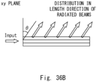
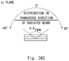
- a light deflection device analysis of a radiated light beam by a light deflection device is performed based on a situation in which light is radiated upward from a photonic crystal waveguide as depicted in Fig. 36A .
- the above-described photonic crystal waveguide has a symmetric structure that is symmetrical with respect to the thickness direction of the waveguide. Due to the symmetric structure of the photonic crystal waveguide, even when the side of the waveguide from which the radiated light beam to be used by the light deflection device is radiated is defined as an upward orientation, radiation of light occur in a up-and-down symmetrical manner with respect to the photonic crystal.
- the side wall is perpendicular and the diameters of the apertures at the upper and lower ends in the thickness direction are identical with each other and the cross-sectional shape is upward-and downward symmetrical in the thickness direction.
- air exists above an SiO 2 cladded material covering the Si slab where the waveguide is formed, and an Si substrate exists below it. In this calculation as well, such air and a substrate are assumed.
- Patent Literatures 2 and 3 a configuration is known according to which point-like defects are provided in addition to the linear defect, the cross-sectional shape of these point-like defects are made up-and-down asymmetrical with reference to the slab surface, and thereby the ratio of the amounts of light radiated upward and downward is changed for the radiated light extracted from the linear defect to the point-like defects.
- the configuration of Patent Literature 2 is such that the point-like defects are provided independently of the waveguide through the linear defect so as to perform branching and coupling and, the configuration of Patent Literature 3 is directed to improve the efficiency of extraction of light with a particular wavelength.
- An object of the present invention is to improve the radiation efficiency of the radiated light beams in a light deflection device.
- a light deflection device of the present invention is defined in claim 1. It is configured by a photonic crystal waveguide having a lattice array with low refractive index parts periodically arranged in a surface of a high refractive-index member.
- This lattice array includes a dual-periodic structure including a first periodic array and a second periodic array different from each other in periodic arrangement of the low refractive index parts, and a linear defect devoid of the low refractive index parts constitutes a waveguide core that propagates incident light.
- the low refractive index parts have an asymmetrical cross-sectional shape with reference to a thickness direction in at least either of the first and second periodic arrays of the dual-periodic structure.
- the asymmetrical cross-sectional shape By virtue of the asymmetrical cross-sectional shape, the sized on both side in the thickness direction of the low refractive index parts are differentiated from each other and, if the low refractive index parts are circular holes, one side in the thickness direction will have a large diameter and the other side a small diameter.
- the wall surface between one end and the other end in the thickness direction of the low refractive index parts is defined by two sloping surfaces and one horizontal surface.
- One sloping surface and the other sloping surface are coupled via the horizontal surface and thus a stepped cross section is defined.
- the perpendicular wall surface may be configured by the sidewall of cylindrical circular holes, in addition to which the perpendicular wall surface may be configured by shallowly cutting part of the surfaces of the low refractive index parts and the high refractive-index member to form a groove and the side wall of this groove can be used to define the perpendicular wall surface.
- the dual periodicity implemented on the lattice array of the photonic crystal waveguide of the present invention includes the first periodic array and the second periodic array that differ from each other in the periodic arrangement. If the periodically arranged low refractive index parts are configured by circular holes, then the different periodic arrays that achieve the dual periodicity can be configured by the following modes of period modulation (Ba) and (Bb):
- circular holes differing in the diameter 2r are arranged in the individual low refractive index parts of the first periodic array and the second periodic array.
- the circular holes are arranged at predetermined intervals in the propagation direction of the waveguide of the individual periodic arrays, and the circular holes of the first periodic array and the circular holes of the second periodic array are alternately arranged in the row extending in the propagation direction of the waveguide.
- the ratio of radiation and the radiation rate can be controlled by adjusting the angle of inclination of the sloping surface of the radiation side and the depth of the perpendicular surface.
- the ratio of radiation is a ratio of the light power of the light radiated on both sides in the thickness direction and indicates the unidirectional radiation property. If the thickness direction is expressed as the upward-downward direction of the radiated light of the light deflection device, then the ratio of radiation is expressed as a ratio Pupper/Plower between the upward light power Pupper and the downward light power Plower.
- the radiation rate is, in the slow light waveguide, the radiation coefficient by which the radiated light beams are radiated in the propagation direction and it is preferable that light is radiated within the range of, for example, 10 1 dB/cm to 10 2 dB/cm.
- the ratio of radiation according to which the amount of radiation from the side of the large aperture diameter becomes large if the angle of inclination of the sloping surface is a small angle, can be changed to such a ratio of radiation that the amount of radiation from the side of the small aperture diameter is large by inverting the ratio of radiation by setting the angle of inclination of the sloping surface to a large angle closer to 90° of the perpendicular wall.
- both of the small-diameter and large-diameter circular holes are configured to have an asymmetrical cross-sectional shape. According to the third mode of asymmetry, the ratio of radiation from the side of the small aperture diameter can be increased.
- the modulation is achieved by the dual periodic structure in which the intervals of arrangement of the circular holes repeatedly appear with grating pitches with different lengths in the propagation direction.
- the first periodic array and the second periodic array are arranged with a positional gap relative to each other in the propagation direction of the waveguide, and the circular holes in the lattice array are repeatedly arranged with the grating pitches with different lengths in the propagation direction of the waveguide.
- the ratio of radiation can be controlled by making the cross-sectional shape of the circular holes asymmetrical and the unidirectional radiation property can be improved.
- the second mode of arrangement is a mode which makes the cross-sectional shape asymmetrical by adjusting the aperture diameter of the circular holes residing at a particular periodic locations.
- the section (b) of Fig. 1A illustrates an example of ⁇ 2r dual periodic structure based on circular holes having different diameters.
- circular holes 20 having different diameters embedded in SiO 2 are arranged with a period twice as long as the grating constant "a" on both side of the Si slab of the photonic crystal waveguide 2 with the waveguide core 12 residing in between.
- the periodically arranged circular holes 20 includes small-diameter circular holes 21 having a diameter of 2r1 and large-diameter circular holes 22 having a diameter of 2r2 (where r2 > r1).
- the small-diameter circular holes 21 and the large-diameter circular holes 22 are respectively arranged with a period twice as long as the grating constant a.
- the light deflection device 1 of the present invention includes, in the lattice array 3, a dual periodic structure including a first periodic array and a second periodic array in which the low refractive index parts 11 are periodically arranged.
- the dual periodic structure contributes to the diffraction function to modulate the radiated light, deflect the propagating light that propagates in the waveguide core 12, and radiate the radiated light beam to the outside; and the function to reduce the dependence of the transverse angle distribution of the radiated light beam upon the wavelength and the refractive index so as to provide homogeneous light beams in a wide angle in the transverse direction.
- the first periodic array and the second periodic array are arranged with a positional gap with respect to each other in the propagation direction of the waveguide, and in the rows of the low refractive index parts arranged in the propagation direction of the waveguide, the low refractive index parts of the circular holes having the same diameter are repeatedly arranged with grating pitches of different lengths in the propagation direction of the waveguide.
- the ⁇ 2r dual periodic modulation achieves modulation through the dual periodic structure in which circular holes of two types with different diameters appear repeatedly.
- the dual periodic structure may consist of, for example, a periodic structure in which large-diameter circular holes repeatedly appear and a periodic structure in which small-diameter circular holes repeatedly appear.
- the large diameter and the small diameter of the circular holes constituting the dual periodic structure reflect their magnitude relationship with respect to the diameter of the reference circular hole or in the context of comparison of these diameters with each other and, with regard to the diameters of the individual circular holes, for example, if the diameter of the reference circular hole is 2r and the diameter difference between the diameters is 2 ⁇ r, then the diameter 2r1 of the large-diameter circular holes is 2(r + ⁇ r) and the diameter 2r2 of the small-diameter circular holes is 2(r - ⁇ r).
- FIGs. 2E and 2F which illustrate the fourth mode of arrangement, in the same manner as in the first mode of arrangement, circular holes are arranged in a V-shape or an inverted V-shape, in addition to which, with regard the periodic sections of two types of the dual periodic structure, the sizes of the circular holes of the low refractive index parts are arranged in a gradational fashion so that the V-shape or inverted V-shape and the gradational arrangement are employed in combination with each other.
- the fifth mode of arrangement is illustrated which is a mode of arrangement that merges the forms of a V-shape and an inverted V-shape.
- the sixth mode of arrangement is illustrated which is a mode in which the linear arrangements of the circular holes of two types are alternately arranged in the transverse direction orthogonal to the propagation direction of the waveguide.
- the first mode of arrangement is a mode of arrangement in which, for the entire lattice array, the circular holes are arranged with different grating pitches
- the section (a) of Fig. 3 illustrates an example of the lattice array in which circular holes are triangularly arranged
- the section (b) of Fig. 3 illustrates an example where the circular holes are arranged in a V-shape.
- the section (c) illustrates an example where, grating-pitch dual periodic structure is adopted for the circular holes of the first row adjacent to the waveguide in the lattice array having triangularly arranged circular holes
- the section (d) of Fig. 3 illustrates an example where the grating-pitch dual periodic structure is adopted for the circular holes of the second row from the waveguide in the lattice array having triangularly arranged circular holes.
- the section (e) illustrates an example where the grating-pitch dual periodic structure is adopted for the first to third rows from the waveguide in the lattice array having triangularly arranged circular holes
- the section (f) of Fig. 3 illustrates an example where the grating-pitch dual periodic structure is adopted for the first to third rows from the waveguide in the lattice array of circular holes arranged in a V-shape.
- the fourth mode of arrangement is a mode of arrangement in which the dual periodicity based upon the grating pitches and the dual periodicity based upon the diameters of the circular holes are combined on the lattice array.
- the section (g) illustrates an example where the dual periodic structure based upon the different grating pitches is adopted for the first row from the waveguide in the lattice array having triangularly arranged circular holes, and the different-diameter dual periodic structure is adopted for the second row from the waveguide.
- the section (h) illustrates an example where a dual periodic structure based on different grating pitches is adopted for the first and third rows from the waveguide in the lattice array having triangularly arranged circular holes, and the different-diameter dual periodic structure is adopted with regard to the second and fourth rows from the waveguide.
- Figs. 4A to 4G are examples where the cross-sectional shape of the small-diameter circular holes are asymmetrical in the ⁇ 2r dual periodic structure based on the circular holes differing in their diameters
- Fig. 4H is an example where the cross-sectional shape of the small-diameter circular holes is asymmetrical in the ⁇ a dual periodic structure based on the arrangement of the circular holes differing in their grating pitches.
- the asymmetrical cross-sectional shape may take multiple forms and the side walls defining the asymmetrical cross-sectional shape may have a wall shape of various forms such as the form of an inclined wall with respect to the thickness direction, a stepped wall defined by at least two walls selected from an inclined wall, a perpendicular wall, and a horizontal wall, and the like.
- the fifth mode is a mode in which the side wall defining the asymmetrical cross-sectional shape is defined by a stepped wall that is stepped in the thickness direction.
- the wall surface between one end and the other end is defined by a sloping surface, a horizontal surface, and a perpendicular surface in the thickness direction of the low refractive index parts; and the sloping surface of the large aperture diameter and the perpendicular surface of the small aperture diameter are coupled via the horizontal surface and thus configured.
- the sixth mode is a mode in which the side wall defining the asymmetrical cross-sectional shape is defined by a stepped wall that is stepped in the thickness direction.
- the wall surface between one end and the other end is defined by a perpendicular surface, a horizontal surface, and a sloping surface in the thickness direction of the low refractive index parts, and the perpendicular surface of the large aperture diameter and the sloping surface whose aperture diameter is small are coupled via the horizontal surface and thus configured.
- the seventh mode is a mode in which the side wall defining the asymmetrical cross-sectional shape is defined by a stepped wall that is stepped in the thickness direction.
- Fig. 4G in the context of the cross-sectional shape of the stepped wall of the seventh mode, by providing a groove section on one side in the sloping surface coupling the upper side and the lower side in the thickness direction of the low refractive index parts, the diameter of one side of the sloping surface is enlarged to impart asymmetry thereto.
- the eighth mode is a mode in which the side wall defining the asymmetrical cross-sectional shape is defined by an inclined wall that is inclined with respect to the thickness direction in the ⁇ a dual periodic structure based on the arrangement of the circular holes differing in their grating pitches.
- the wall surface between one end and the other end is defined by a sloping surface in the thickness direction, and the cross-sectional shape of the low refractive index parts has a trapezoidal shape.
- the wall surface between one end and the other end in the thickness direction are defined by a perpendicular surface
- the low refractive index parts has a cylindrical shape
- the cross-sectional shape has a rectangular shape.
- Figs. 4A to 4H examples are illustrated where the cross-sectional shape of the small-diameter circular holes is asymmetrical, but the configuration may be such that the cross-sectional shape of the large-diameter circular holes is a shape asymmetrical in the thickness direction and, alternatively, the configuration may be such that the cross-sectional shape of both of the small-diameter and large-diameter circular holes is a shape asymmetrical in the thickness direction. It should be noted that, in this case, the radiation efficiency will exhibit different unidirectional radiation property.
- the section (d) depicts the cross section of the light deflection device of the present invention, where the x-direction is a direction orthogonal to the propagation direction of the slow light propagating in the waveguide and the z-direction is the thickness direction of the lamination constituting the light deflection device.
- the lattice array 3 sandwiched by SiO 2 cladded materials 13 on the upper and lower sides, is provided.
- the lattice array 3 is configured by arranging the low refractive index parts 11 at predetermined intervals within the high refractive-index member 10.
- the low refractive index parts 11 are configured by 2r1 small-diameter circular holes 21 and the 2r2 large-diameter circular holes 22 having different diameters. It should be noted that, in the lattice array 3, the linear defect in which no low refractive index parts are arranged constitutes the waveguide.
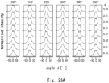
- the sections (a) to (c) are diagrams in which the lattice array 3 of the light deflection device is viewed in the x-y plane, and the sections (a) and (b) of Fig. 5 illustrates examples of a traditional transverse-row array and a V-shape arrangement in the ⁇ 2r dual periodic modulation, and the section (c) of Fig. 5 illustrates an example of the ⁇ a dual periodic modulation. Also, the locations on which DFT analysis and monitoring are performed and the locations to be subjected to excitation during the calculation are indicated by the symbol "x.” It should be noted that, in the sections (a) and (b) of Fig.
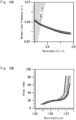
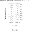
- Fig. 7A indicates normalized frequency a/ ⁇ for wave number (2 ⁇ /a)
- Fig. 7B indicates group refractive index for wavelength ( ⁇ m)
- Fig. 7C indicates radiation coefficient (scattering loss) (dB/cm) for wavelength ( ⁇ m)
- Fig. 7D indicates ratio of radiation Pupper/Plower for wavelength ( ⁇ m).
- Fig. 7E indicates the cross-sectional shape.
- a ratio of 2.5:1 or more is obtained when the angle of inclination ⁇ g falls within the range of 65° to 87°.
- a substantially 2:1 ratio can be obtained when the angle of inclination ⁇ g falls within the range of 75° to 85°.
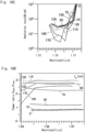
- Figs. 11A to 11E illustrate an example mode where the side walls of the small-diameter and the large-diameter circular holes are inclined walls in the ⁇ 2r dual periodic modulation and the lattice array according to the V-shape arrangement.
- the pieces of characteristic data shown in Figs. 11A to 11E reflect the case where the diameter difference ⁇ 2r of the ⁇ 2r dual-periodicity diameter is set to 10 nm, and the angle of inclination ⁇ g of the inclined wall is changed within the range of 60° to 90°.
- the ratio of radiation of Fig. 11D when the angle of inclination ⁇ g falls within the range of 60° to 90°, the ratio of radiation is not larger than 1, and radiation takes place mainly downward.
- Fig. 12 illustrates an example mode where the side walls of the small-diameter circular holes are inclined walls in the ⁇ 2r dual periodic modulation and the lattice array of transverse-row array. It should be noted that, in the transverse-row array, the circular holes are triangularly arranged, and the small diameters and large diameters are arranged in the transverse direction orthogonal to the propagation direction.
- ⁇ a dual periodic modulation is performed only for the first low close to the waveguide, and the circular holes are arranged with repeated long and short grating pitches and, further, in the first row, the side walls of only the positionally-deviated circular holes or only the circular holes that were not positionally-deviated are provided as an inclined wall.
- the section (a) is a cross-sectional view
- the section (b) of Fig. 18 is a schematic perspective view. In the example mode of Fig.
- the side wall is configured as an inclined wall and the cross-sectional shape thereof is made asymmetrical only for the circular holes of one periodic array.
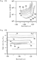
- Figs. 20A and 20B in the case where the inclined wall whose angle of inclination ⁇ g falls within the range of 75 to 85°, the radiated light beams exhibit the tendency of monomodality as compared with the case where the angle of inclination ⁇ g is 90° (perpendicular wall).
- "k" of Figs. 20A and 20B represents the wave number of light, change of which corresponds to the wavelength of the light is being changed or changing the deflection angle of the light in the traveling direction.
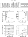
- the sections (a) and (b) illustrate the case where the first to tenth rows in the lattice array according to the V-shape arrangement are subjected to the ⁇ 2r dual periodic modulation and the angle of inclination ⁇ g is set to 90° which corresponds to an angle of a perpendicular wall, and the case where the angle of inclination ⁇ g is set to 80°, the sections (c) and (d) of Fig.
- FIG. 21 illustrate the case where the first to tenth rows in the lattice array of normal transverse-row arrangement are subjected to the ⁇ 2r dual periodic modulation and the angle of inclination ⁇ g is set to 90° which corresponds to an angle of a perpendicular wall, and the case where the angle of inclination ⁇ g is set to 80°, the sections (e) and (f) of Fig. 21 illustrate the case where only the first row in the lattice array is subjected to ⁇ a dual periodic modulation and the angle of inclination ⁇ g is set to 90° which corresponds to an angle of a perpendicular wall, and the case where the angle of inclination ⁇ g is set to 80°.
- the electric field strength distribution of radiation components of Fig. 21 is obtained by performing inverse Fourier transform on the intensity of the radiated beams, and thereby converting them into the mode pattern on the waveguide.
- This mode pattern serves as an indicator for determining in which of the modes the components contributing to the radiated beam are found.
- the mode patterns exist in the range of about three rows among the linear rows of the circular holes from the central waveguide to the outside, and this figure indicates that the dual periodic modulation work effectively within this range. It should be noted that, in Fig. 21 , as the mode pattern where the wave number k is 0.39 and 0.41 are out of the range of use as a light deflector, the mode patterns where the wave number k is 0.43 to 0.49 are meaningful in the context of the light deflector.
Landscapes
- Physics & Mathematics (AREA)
- General Physics & Mathematics (AREA)
- Optics & Photonics (AREA)
- Nonlinear Science (AREA)
- Engineering & Computer Science (AREA)
- Microelectronics & Electronic Packaging (AREA)
- Optical Integrated Circuits (AREA)
- Optical Modulation, Optical Deflection, Nonlinear Optics, Optical Demodulation, Optical Logic Elements (AREA)
Claims (9)
- Lichtablenkungsvorrichtung (1) mit einem photonischen Kristallwellenleiter (2), der einen Wellenleiterkern (12) und eine Gitteranordnung (3) mit Teilen (11) mit niedrigem Brechungsindex aufweist, die periodisch in einer Oberfläche eines Elements (10) mit hohem Brechungsindex angeordnet sind, wobei der Wellenleiterkern (12) durch Bereitstellen eines Abschnitts ohne die Teile mit niedrigem Brechungsindex konfiguriert ist, wobei sich Licht in dem Wellenleiterkern (12) in der Längsrichtung ausbreitet und über den Wellenleiterkern (12) nach außen abgestrahlt wird, wobeidie Gitteranordnung (3) eine doppelt-periodische Struktur aufweist, die eine erste periodische Anordnung und eine zweite periodische Anordnung umfasst, die sich in der periodischen Anordnung der Teile (11) mit niedrigem Brechungsindex voneinander unterscheiden, dadurch gekennzeichnet, dassdie Teile (11) mit niedrigem Brechungsindex eine asymmetrische Querschnittsform in Bezug auf eine Dickenrichtung in mindestens einer der ersten und zweiten periodischen Anordnungen der doppelperiodischen Struktur aufweisen und dadurch die Intensität der Lichtstrahlung in einer Richtung einer Dickenrichtung erhöhen.
- Lichtablenkungsvorrichtung (1) nach Anspruch 1, wobei die Seitenwände der Teile (11) mit niedrigem Brechungsindex, die die asymmetrische Querschnittsform aufweisen, jeweils eine Wandform entweder einer geneigten Wand oder einer gestuften Wand in einer Dickenrichtung haben, wobei die gestufte Wand durch mindestens zwei Wände definiert ist, die aus der Gruppe ausgewählt sind, die aus einer geneigten Wand, einer senkrechten Wand und einer horizontalen Wand besteht.
- Lichtablenkungsvorrichtung (1) nach Anspruch 1 oder 2, wobei die doppelt-periodische Struktur so konfiguriert ist, dass:kreisförmige Löcher (20) mit unterschiedlichen Durchmessern in den Teilen (11) mit niedrigem Brechungsindex der ersten periodischen Anordnung und der zweiten periodischen Anordnung angeordnet sind;die kreisförmigen Löcher (20) in vorbestimmten Abständen in einer Ausbreitungsrichtung des Wellenleiters angeordnet sind, der die periodischen Anordnungen umfasst;die kreisförmigen Löcher (20) der ersten periodischen Anordnung und die kreisförmigen Löcher (20) der zweiten periodischen Anordnung abwechselnd in Reihen angeordnet sind, die sich in der Ausbreitungsrichtung des Hohlleiters (2) erstrecken; undvon den kreisförmigen Löchern (22) mit großem Durchmesser und kreisförmigen Löchern (21) mit kleinem Durchmesser, die sich im Durchmesser voneinander unterscheiden, die kreisförmigen Löcher (21) mit kleinem Durchmesser eine asymmetrische Querschnittsform aufweisen.
- Lichtablenkungsvorrichtung (1) nach Anspruch 1 oder 2, wobei die doppelt-periodische Struktur so gestaltet ist, dass:kreisförmige Löcher (20) mit unterschiedlichen Durchmessern in den Teilen (11) mit niedrigem Brechungsindex der ersten periodischen Anordnungen und der zweiten periodischen Anordnung angeordnet sind;die kreisförmigen Löcher (20) in vorbestimmten Abständen in einer Ausbreitungsrichtung des Wellenleiters (2) angeordnet sind, der die periodische Anordnung umfasst;die kreisförmigen Löcher (20) der ersten periodischen Anordnung und die kreisförmigen Löcher der zweiten periodischen Anordnung abwechselnd in Reihen angeordnet sind, die sich in der Ausbreitungsrichtung des Hohlleiters (2) erstrecken; undaus den kreisförmigen Löchern (22) mit großem Durchmesser und den kreisförmigen Löchern (21) mit kleinem Durchmesser, die sich im Durchmesser voneinander unterscheiden, die kreisförmigen Löcher (22) mit großem Durchmesser eine asymmetrische Querschnittsform aufweisen.
- Lichtablenkungsvorrichtung (1) nach Anspruch 1 oder 2, wobei die doppelt-periodische Struktur so gestaltet ist, dass:die kreisförmigen Löcher (20) mit den unterschiedlichen Durchmessern in den Teilen (11) mit niedrigem Brechungsindex der ersten periodischen Anordnung und der zweiten periodischen Anordnung angeordnet sind;die kreisförmigen Löcher (20) in vorbestimmten Abständen in einer Ausbreitungsrichtung des Wellenleiters angeordnet sind, der die periodischen Anordnungen umfasst;die kreisförmigen Löcher (20) der ersten periodischen Anordnung und die kreisförmigen Löcher (20) der zweiten periodischen Anordnung abwechselnd in Reihen angeordnet sind, die sich in der Ausbreitungsrichtung des Hohlleiters (2) erstrecken; undsich die kreisförmigen Löcher (22) mit großem Durchmesser und die kreisförmigen Löcher (21) mit kleinem Durchmesser im Durchmesser voneinander unterscheiden und eine asymmetrische Querschnittsform aufweisen.
- Lichtablenkungsvorrichtung (1) nach Anspruch 1 oder 2, wobei die doppelt-periodische Struktur so konfiguriert ist, dass:die kreisförmigen Löcher (20) mit unterschiedlichen Durchmessern in den Teilen (11) mit niedrigem Brechungsindex der ersten periodischen Anordnung und der zweiten periodischen Anordnung angeordnet sind, wobei die kreisförmigen Löcher in vorgegebenen Abständen in Ausbreitungsrichtung eines Wellenleiters (2) der periodischen Anordnungen angeordnet sind;die kreisförmigen Löcher (20) der ersten periodischen Anordnung und die kreisförmigen Löcher der zweiten periodischen Anordnung abwechselnd in der gleichen Reihe angeordnet sind, die sich in der Ausbreitungsrichtung des Hohlleiters (2) erstreckt; unddie kreisförmigen Löcher (20) jeder periodischen Anordnung der ersten periodischen Anordnung und der zweiten periodischen Anordnung eine asymmetrische Querschnittsform aufweisen.
- Lichtablenkungsvorrichtung (1) nach Anspruch 3 oder 6, wobei die periodische Anordnung der kreisförmigen Löcher (20) mit der asymmetrischen Querschnittsform eine periodische Anordnung der zweiten Reihe aus einem Zeilendefekt ohne die kreisförmigen Löcher zwischen den Reihen in der Ausbreitungsrichtung des Hohlleiters (2) ist.
- Lichtablenkungsvorrichtung (1) nach Anspruch 3 oder 6, wobei unter den kreisförmigen Löchern (20), die in der Gitteranordnung (3) vorgesehen sind, die doppelt-periodischen kreisförmigen Löcher der geradzahligen Gitterreihen in Ausbreitungsrichtung des Hohlleiters (2) einen vergrößerten oder verkleinerten Durchmesser im Vergleich zu den kreisförmigen Löchern (20) an anderen Stellen aufweisen.
- Lichtablenkungsvorrichtung (1) nach Anspruch 2, wobei die senkrechte Wandfläche eine Seitenwand einer Nut ist, die durch Entfernen eines Teils der Oberflächen einer Vielzahl der Teile mit niedrigem Brechungsindex, die eine asymmetrische Querschnittsform haben, und des Elements (10) mit hohem Brechungsindex gebildet ist.
Applications Claiming Priority (2)
| Application Number | Priority Date | Filing Date | Title |
|---|---|---|---|
| JP2017160825 | 2017-08-24 | ||
| PCT/JP2018/031052 WO2019039526A1 (ja) | 2017-08-24 | 2018-08-22 | 光偏向デバイス |
Publications (3)
| Publication Number | Publication Date |
|---|---|
| EP3674760A1 EP3674760A1 (de) | 2020-07-01 |
| EP3674760A4 EP3674760A4 (de) | 2021-04-21 |
| EP3674760B1 true EP3674760B1 (de) | 2024-07-10 |
Family
ID=65439109
Family Applications (1)
| Application Number | Title | Priority Date | Filing Date |
|---|---|---|---|
| EP18848805.0A Active EP3674760B1 (de) | 2017-08-24 | 2018-08-22 | Lichtablenkungsvorrichtung |
Country Status (5)
| Country | Link |
|---|---|
| US (1) | US11067746B2 (de) |
| EP (1) | EP3674760B1 (de) |
| JP (1) | JP7134443B2 (de) |
| CN (1) | CN111164477B (de) |
| WO (1) | WO2019039526A1 (de) |
Families Citing this family (2)
| Publication number | Priority date | Publication date | Assignee | Title |
|---|---|---|---|---|
| DE112022002553B4 (de) * | 2021-07-14 | 2025-02-27 | Ngk Insulators, Ltd. | Optische abtastvorrichtung |
| WO2024073151A1 (en) * | 2022-09-30 | 2024-04-04 | Purdue Research Foundation | Optical phased array gratings based on extreme skin-depth metamaterial waveguides |
Family Cites Families (18)
| Publication number | Priority date | Publication date | Assignee | Title |
|---|---|---|---|---|
| JP3925769B2 (ja) | 2000-03-24 | 2007-06-06 | 関西ティー・エル・オー株式会社 | 2次元フォトニック結晶及び合分波器 |
| TW574588B (en) * | 2001-03-22 | 2004-02-01 | Matsushita Electric Works Ltd | Light-beam deflecting device with photonic crystal, optical switch using the same, and light-beam deflecting method |
| JP4219668B2 (ja) * | 2001-12-13 | 2009-02-04 | パナソニック株式会社 | フォトニック結晶の作製方法及び光デバイス作製方法 |
| JPWO2003081303A1 (ja) | 2002-03-27 | 2005-07-28 | 三菱電機株式会社 | 光学素子の製造方法 |
| JP2004258169A (ja) * | 2003-02-25 | 2004-09-16 | Alps Electric Co Ltd | 光偏向素子及びそれを用いた光スイッチ |
| JP3999152B2 (ja) | 2003-03-25 | 2007-10-31 | アルプス電気株式会社 | 2次元フォトニック結晶スラブ及びこれを用いた光デバイス |
| JP2005208180A (ja) | 2004-01-21 | 2005-08-04 | Nikon Corp | 光学素子の製造方法 |
| US7054524B2 (en) | 2004-08-30 | 2006-05-30 | Energy Conversion Devices, Inc. | Asymmetric photonic crystal waveguide element having symmetric mode fields |
| JP4534036B2 (ja) | 2004-09-08 | 2010-09-01 | 国立大学法人京都大学 | 光ヘッド及び光記録再生装置 |
| JP2006184618A (ja) | 2004-12-28 | 2006-07-13 | Kyoto Univ | 2次元フォトニック結晶及びそれを用いた光機能素子 |
| US7630604B2 (en) * | 2006-10-26 | 2009-12-08 | The Board Of Trustees Of The Leland Stanford Junior University | Dipole induced transparency drop-filter cavity-waveguide system |
| JP4971045B2 (ja) | 2007-06-15 | 2012-07-11 | 株式会社リコー | 光制御素子 |
| US9535308B2 (en) * | 2013-09-25 | 2017-01-03 | Oracle International Corporation | Enhanced optical modulation using slow light |
| WO2016008771A1 (en) * | 2014-07-14 | 2016-01-21 | University Of Copenhagen | Optical device having efficient light-matter interface for quantum simulations |
| CN104252019B (zh) * | 2014-10-15 | 2017-04-19 | 山东大学 | 一种二维组合型光子晶体及其应用 |
| US10215918B2 (en) | 2015-11-24 | 2019-02-26 | Omega Optics, Inc. | Subwavelength photonic crystal waveguide in optical systems |
| CN108700790B (zh) * | 2016-01-22 | 2021-10-22 | 国立大学法人横浜国立大学 | 光偏转器及激光雷达装置 |
| JP6675889B2 (ja) | 2016-03-08 | 2020-04-08 | 三菱重工業株式会社 | 動弁装置及びクロスヘッド式内燃機関 |
-
2018
- 2018-08-22 WO PCT/JP2018/031052 patent/WO2019039526A1/ja not_active Ceased
- 2018-08-22 EP EP18848805.0A patent/EP3674760B1/de active Active
- 2018-08-22 JP JP2019537667A patent/JP7134443B2/ja active Active
- 2018-08-22 CN CN201880062107.5A patent/CN111164477B/zh active Active
- 2018-08-22 US US16/641,217 patent/US11067746B2/en active Active
Also Published As
| Publication number | Publication date |
|---|---|
| US11067746B2 (en) | 2021-07-20 |
| CN111164477B (zh) | 2022-07-05 |
| WO2019039526A1 (ja) | 2019-02-28 |
| EP3674760A4 (de) | 2021-04-21 |
| EP3674760A1 (de) | 2020-07-01 |
| CN111164477A (zh) | 2020-05-15 |
| JP7134443B2 (ja) | 2022-09-12 |
| US20200225411A1 (en) | 2020-07-16 |
| JPWO2019039526A1 (ja) | 2020-10-15 |
Similar Documents
| Publication | Publication Date | Title |
|---|---|---|
| JP6879561B2 (ja) | 光偏向デバイスおよびライダー装置 | |
| JP7076822B2 (ja) | 光受信器アレイ、及びライダー装置 | |
| JP3846228B2 (ja) | 導波路 | |
| JP3459827B2 (ja) | 2次元フォトニック結晶光分合波器 | |
| US7116878B2 (en) | Optical waveguide structure | |
| EP3674760B1 (de) | Lichtablenkungsvorrichtung | |
| Cakmak et al. | High efficiency of graded index photonic crystal as an input coupler | |
| CN114153029A (zh) | 一种基于连续域束缚态的光栅结构 | |
| US6782169B2 (en) | System for efficient coupling to photonic crystal waveguides | |
| CN1449507A (zh) | 声光可调谐滤波器 | |
| Tanaka et al. | Analysis of a line-defect waveguide on a silicon-on-insulator two-dimensional photonic-crystal slab | |
| US6836494B1 (en) | Structure and method for processing optical energy | |
| JP3999152B2 (ja) | 2次元フォトニック結晶スラブ及びこれを用いた光デバイス | |
| JP6883828B2 (ja) | 光偏向デバイス | |
| TWI292496B (de) | ||
| JP6931237B2 (ja) | 光偏向デバイス、及びライダー装置 | |
| Feng et al. | Tuning beam power-splitting characteristics through modulating a photonic crystal slab’s output surface | |
| JP2003156642A (ja) | 光導波路およびその製造方法 | |
| US12066739B2 (en) | Optical scanner | |
| JP6945816B2 (ja) | 光偏向デバイス | |
| KR102223750B1 (ko) | 광의 위상을 가변할 수 있는 배열 안테나 | |
| Li et al. | Probing photonic crystals on silicon-on-insulator with Ge∕ Si self-assembled islands as an internal source | |
| EP2058643B1 (de) | Berührungslose Messsonde | |
| US12321011B2 (en) | Turning grating device for emission of arbitrary optical beam profiles from waveguides into two-dimensional space | |
| JP4956741B2 (ja) | フォトニック結晶導波路 |
Legal Events
| Date | Code | Title | Description |
|---|---|---|---|
| STAA | Information on the status of an ep patent application or granted ep patent |
Free format text: STATUS: THE INTERNATIONAL PUBLICATION HAS BEEN MADE |
|
| PUAI | Public reference made under article 153(3) epc to a published international application that has entered the european phase |
Free format text: ORIGINAL CODE: 0009012 |
|
| STAA | Information on the status of an ep patent application or granted ep patent |
Free format text: STATUS: REQUEST FOR EXAMINATION WAS MADE |
|
| 17P | Request for examination filed |
Effective date: 20200304 |
|
| AK | Designated contracting states |
Kind code of ref document: A1 Designated state(s): AL AT BE BG CH CY CZ DE DK EE ES FI FR GB GR HR HU IE IS IT LI LT LU LV MC MK MT NL NO PL PT RO RS SE SI SK SM TR |
|
| AX | Request for extension of the european patent |
Extension state: BA ME |
|
| DAV | Request for validation of the european patent (deleted) | ||
| DAX | Request for extension of the european patent (deleted) | ||
| A4 | Supplementary search report drawn up and despatched |
Effective date: 20210324 |
|
| RIC1 | Information provided on ipc code assigned before grant |
Ipc: G02B 6/122 20060101AFI20210318BHEP Ipc: G02F 1/29 20060101ALI20210318BHEP |
|
| GRAP | Despatch of communication of intention to grant a patent |
Free format text: ORIGINAL CODE: EPIDOSNIGR1 |
|
| STAA | Information on the status of an ep patent application or granted ep patent |
Free format text: STATUS: GRANT OF PATENT IS INTENDED |
|
| INTG | Intention to grant announced |
Effective date: 20240326 |
|
| GRAS | Grant fee paid |
Free format text: ORIGINAL CODE: EPIDOSNIGR3 |
|
| GRAA | (expected) grant |
Free format text: ORIGINAL CODE: 0009210 |
|
| STAA | Information on the status of an ep patent application or granted ep patent |
Free format text: STATUS: THE PATENT HAS BEEN GRANTED |
|
| AK | Designated contracting states |
Kind code of ref document: B1 Designated state(s): AL AT BE BG CH CY CZ DE DK EE ES FI FR GB GR HR HU IE IS IT LI LT LU LV MC MK MT NL NO PL PT RO RS SE SI SK SM TR |
|
| REG | Reference to a national code |
Ref country code: CH Ref legal event code: EP |
|
| REG | Reference to a national code |
Ref country code: DE Ref legal event code: R096 Ref document number: 602018071680 Country of ref document: DE |
|
| REG | Reference to a national code |
Ref country code: LT Ref legal event code: MG9D |
|
| REG | Reference to a national code |
Ref country code: NL Ref legal event code: MP Effective date: 20240710 |
|
| PG25 | Lapsed in a contracting state [announced via postgrant information from national office to epo] |
Ref country code: PT Free format text: LAPSE BECAUSE OF FAILURE TO SUBMIT A TRANSLATION OF THE DESCRIPTION OR TO PAY THE FEE WITHIN THE PRESCRIBED TIME-LIMIT Effective date: 20241111 |
|
| REG | Reference to a national code |
Ref country code: AT Ref legal event code: MK05 Ref document number: 1702536 Country of ref document: AT Kind code of ref document: T Effective date: 20240710 |
|
| PG25 | Lapsed in a contracting state [announced via postgrant information from national office to epo] |
Ref country code: NL Free format text: LAPSE BECAUSE OF FAILURE TO SUBMIT A TRANSLATION OF THE DESCRIPTION OR TO PAY THE FEE WITHIN THE PRESCRIBED TIME-LIMIT Effective date: 20240710 |
|
| PG25 | Lapsed in a contracting state [announced via postgrant information from national office to epo] |
Ref country code: PT Free format text: LAPSE BECAUSE OF FAILURE TO SUBMIT A TRANSLATION OF THE DESCRIPTION OR TO PAY THE FEE WITHIN THE PRESCRIBED TIME-LIMIT Effective date: 20241111 Ref country code: NL Free format text: LAPSE BECAUSE OF FAILURE TO SUBMIT A TRANSLATION OF THE DESCRIPTION OR TO PAY THE FEE WITHIN THE PRESCRIBED TIME-LIMIT Effective date: 20240710 |
|
| PG25 | Lapsed in a contracting state [announced via postgrant information from national office to epo] |
Ref country code: NO Free format text: LAPSE BECAUSE OF FAILURE TO SUBMIT A TRANSLATION OF THE DESCRIPTION OR TO PAY THE FEE WITHIN THE PRESCRIBED TIME-LIMIT Effective date: 20241010 |
|
| PG25 | Lapsed in a contracting state [announced via postgrant information from national office to epo] |
Ref country code: FI Free format text: LAPSE BECAUSE OF FAILURE TO SUBMIT A TRANSLATION OF THE DESCRIPTION OR TO PAY THE FEE WITHIN THE PRESCRIBED TIME-LIMIT Effective date: 20240710 Ref country code: GR Free format text: LAPSE BECAUSE OF FAILURE TO SUBMIT A TRANSLATION OF THE DESCRIPTION OR TO PAY THE FEE WITHIN THE PRESCRIBED TIME-LIMIT Effective date: 20241011 Ref country code: PL Free format text: LAPSE BECAUSE OF FAILURE TO SUBMIT A TRANSLATION OF THE DESCRIPTION OR TO PAY THE FEE WITHIN THE PRESCRIBED TIME-LIMIT Effective date: 20240710 |
|
| PG25 | Lapsed in a contracting state [announced via postgrant information from national office to epo] |
Ref country code: BG Free format text: LAPSE BECAUSE OF FAILURE TO SUBMIT A TRANSLATION OF THE DESCRIPTION OR TO PAY THE FEE WITHIN THE PRESCRIBED TIME-LIMIT Effective date: 20240710 |
|
| PG25 | Lapsed in a contracting state [announced via postgrant information from national office to epo] |
Ref country code: LV Free format text: LAPSE BECAUSE OF FAILURE TO SUBMIT A TRANSLATION OF THE DESCRIPTION OR TO PAY THE FEE WITHIN THE PRESCRIBED TIME-LIMIT Effective date: 20240710 |
|
| PG25 | Lapsed in a contracting state [announced via postgrant information from national office to epo] |
Ref country code: IS Free format text: LAPSE BECAUSE OF FAILURE TO SUBMIT A TRANSLATION OF THE DESCRIPTION OR TO PAY THE FEE WITHIN THE PRESCRIBED TIME-LIMIT Effective date: 20241110 Ref country code: AT Free format text: LAPSE BECAUSE OF FAILURE TO SUBMIT A TRANSLATION OF THE DESCRIPTION OR TO PAY THE FEE WITHIN THE PRESCRIBED TIME-LIMIT Effective date: 20240710 |
|
| PG25 | Lapsed in a contracting state [announced via postgrant information from national office to epo] |
Ref country code: HR Free format text: LAPSE BECAUSE OF FAILURE TO SUBMIT A TRANSLATION OF THE DESCRIPTION OR TO PAY THE FEE WITHIN THE PRESCRIBED TIME-LIMIT Effective date: 20240710 |
|
| PG25 | Lapsed in a contracting state [announced via postgrant information from national office to epo] |
Ref country code: ES Free format text: LAPSE BECAUSE OF FAILURE TO SUBMIT A TRANSLATION OF THE DESCRIPTION OR TO PAY THE FEE WITHIN THE PRESCRIBED TIME-LIMIT Effective date: 20240710 Ref country code: RS Free format text: LAPSE BECAUSE OF FAILURE TO SUBMIT A TRANSLATION OF THE DESCRIPTION OR TO PAY THE FEE WITHIN THE PRESCRIBED TIME-LIMIT Effective date: 20241010 |
|
| PG25 | Lapsed in a contracting state [announced via postgrant information from national office to epo] |
Ref country code: RS Free format text: LAPSE BECAUSE OF FAILURE TO SUBMIT A TRANSLATION OF THE DESCRIPTION OR TO PAY THE FEE WITHIN THE PRESCRIBED TIME-LIMIT Effective date: 20241010 Ref country code: PL Free format text: LAPSE BECAUSE OF FAILURE TO SUBMIT A TRANSLATION OF THE DESCRIPTION OR TO PAY THE FEE WITHIN THE PRESCRIBED TIME-LIMIT Effective date: 20240710 Ref country code: NO Free format text: LAPSE BECAUSE OF FAILURE TO SUBMIT A TRANSLATION OF THE DESCRIPTION OR TO PAY THE FEE WITHIN THE PRESCRIBED TIME-LIMIT Effective date: 20241010 Ref country code: LV Free format text: LAPSE BECAUSE OF FAILURE TO SUBMIT A TRANSLATION OF THE DESCRIPTION OR TO PAY THE FEE WITHIN THE PRESCRIBED TIME-LIMIT Effective date: 20240710 Ref country code: IS Free format text: LAPSE BECAUSE OF FAILURE TO SUBMIT A TRANSLATION OF THE DESCRIPTION OR TO PAY THE FEE WITHIN THE PRESCRIBED TIME-LIMIT Effective date: 20241110 Ref country code: HR Free format text: LAPSE BECAUSE OF FAILURE TO SUBMIT A TRANSLATION OF THE DESCRIPTION OR TO PAY THE FEE WITHIN THE PRESCRIBED TIME-LIMIT Effective date: 20240710 Ref country code: GR Free format text: LAPSE BECAUSE OF FAILURE TO SUBMIT A TRANSLATION OF THE DESCRIPTION OR TO PAY THE FEE WITHIN THE PRESCRIBED TIME-LIMIT Effective date: 20241011 Ref country code: FI Free format text: LAPSE BECAUSE OF FAILURE TO SUBMIT A TRANSLATION OF THE DESCRIPTION OR TO PAY THE FEE WITHIN THE PRESCRIBED TIME-LIMIT Effective date: 20240710 Ref country code: ES Free format text: LAPSE BECAUSE OF FAILURE TO SUBMIT A TRANSLATION OF THE DESCRIPTION OR TO PAY THE FEE WITHIN THE PRESCRIBED TIME-LIMIT Effective date: 20240710 Ref country code: BG Free format text: LAPSE BECAUSE OF FAILURE TO SUBMIT A TRANSLATION OF THE DESCRIPTION OR TO PAY THE FEE WITHIN THE PRESCRIBED TIME-LIMIT Effective date: 20240710 Ref country code: AT Free format text: LAPSE BECAUSE OF FAILURE TO SUBMIT A TRANSLATION OF THE DESCRIPTION OR TO PAY THE FEE WITHIN THE PRESCRIBED TIME-LIMIT Effective date: 20240710 |
|
| REG | Reference to a national code |
Ref country code: CH Ref legal event code: PL |
|
| REG | Reference to a national code |
Ref country code: DE Ref legal event code: R097 Ref document number: 602018071680 Country of ref document: DE |
|
| PG25 | Lapsed in a contracting state [announced via postgrant information from national office to epo] |
Ref country code: DK Free format text: LAPSE BECAUSE OF FAILURE TO SUBMIT A TRANSLATION OF THE DESCRIPTION OR TO PAY THE FEE WITHIN THE PRESCRIBED TIME-LIMIT Effective date: 20240710 Ref country code: RO Free format text: LAPSE BECAUSE OF FAILURE TO SUBMIT A TRANSLATION OF THE DESCRIPTION OR TO PAY THE FEE WITHIN THE PRESCRIBED TIME-LIMIT Effective date: 20240710 Ref country code: SM Free format text: LAPSE BECAUSE OF FAILURE TO SUBMIT A TRANSLATION OF THE DESCRIPTION OR TO PAY THE FEE WITHIN THE PRESCRIBED TIME-LIMIT Effective date: 20240710 |
|
| PG25 | Lapsed in a contracting state [announced via postgrant information from national office to epo] |
Ref country code: LU Free format text: LAPSE BECAUSE OF NON-PAYMENT OF DUE FEES Effective date: 20240822 |
|
| PG25 | Lapsed in a contracting state [announced via postgrant information from national office to epo] |
Ref country code: MC Free format text: LAPSE BECAUSE OF FAILURE TO SUBMIT A TRANSLATION OF THE DESCRIPTION OR TO PAY THE FEE WITHIN THE PRESCRIBED TIME-LIMIT Effective date: 20240710 Ref country code: CH Free format text: LAPSE BECAUSE OF NON-PAYMENT OF DUE FEES Effective date: 20240831 Ref country code: EE Free format text: LAPSE BECAUSE OF FAILURE TO SUBMIT A TRANSLATION OF THE DESCRIPTION OR TO PAY THE FEE WITHIN THE PRESCRIBED TIME-LIMIT Effective date: 20240710 |
|
| PG25 | Lapsed in a contracting state [announced via postgrant information from national office to epo] |
Ref country code: CZ Free format text: LAPSE BECAUSE OF FAILURE TO SUBMIT A TRANSLATION OF THE DESCRIPTION OR TO PAY THE FEE WITHIN THE PRESCRIBED TIME-LIMIT Effective date: 20240710 |
|
| PG25 | Lapsed in a contracting state [announced via postgrant information from national office to epo] |
Ref country code: IT Free format text: LAPSE BECAUSE OF FAILURE TO SUBMIT A TRANSLATION OF THE DESCRIPTION OR TO PAY THE FEE WITHIN THE PRESCRIBED TIME-LIMIT Effective date: 20240710 Ref country code: SK Free format text: LAPSE BECAUSE OF FAILURE TO SUBMIT A TRANSLATION OF THE DESCRIPTION OR TO PAY THE FEE WITHIN THE PRESCRIBED TIME-LIMIT Effective date: 20240710 |
|
| PLBE | No opposition filed within time limit |
Free format text: ORIGINAL CODE: 0009261 |
|
| STAA | Information on the status of an ep patent application or granted ep patent |
Free format text: STATUS: NO OPPOSITION FILED WITHIN TIME LIMIT |
|
| 26N | No opposition filed |
Effective date: 20250411 |
|
| GBPC | Gb: european patent ceased through non-payment of renewal fee |
Effective date: 20241010 |
|
| REG | Reference to a national code |
Ref country code: BE Ref legal event code: MM Effective date: 20240831 |
|
| PG25 | Lapsed in a contracting state [announced via postgrant information from national office to epo] |
Ref country code: GB Free format text: LAPSE BECAUSE OF NON-PAYMENT OF DUE FEES Effective date: 20241010 |
|
| PG25 | Lapsed in a contracting state [announced via postgrant information from national office to epo] |
Ref country code: BE Free format text: LAPSE BECAUSE OF NON-PAYMENT OF DUE FEES Effective date: 20240831 |
|
| PG25 | Lapsed in a contracting state [announced via postgrant information from national office to epo] |
Ref country code: FR Free format text: LAPSE BECAUSE OF NON-PAYMENT OF DUE FEES Effective date: 20240910 |
|
| PG25 | Lapsed in a contracting state [announced via postgrant information from national office to epo] |
Ref country code: IE Free format text: LAPSE BECAUSE OF NON-PAYMENT OF DUE FEES Effective date: 20240822 |
|
| PG25 | Lapsed in a contracting state [announced via postgrant information from national office to epo] |
Ref country code: SE Free format text: LAPSE BECAUSE OF FAILURE TO SUBMIT A TRANSLATION OF THE DESCRIPTION OR TO PAY THE FEE WITHIN THE PRESCRIBED TIME-LIMIT Effective date: 20240710 |
|
| PGFP | Annual fee paid to national office [announced via postgrant information from national office to epo] |
Ref country code: DE Payment date: 20250829 Year of fee payment: 8 |
|
| PG25 | Lapsed in a contracting state [announced via postgrant information from national office to epo] |
Ref country code: CY Free format text: LAPSE BECAUSE OF FAILURE TO SUBMIT A TRANSLATION OF THE DESCRIPTION OR TO PAY THE FEE WITHIN THE PRESCRIBED TIME-LIMIT; INVALID AB INITIO Effective date: 20180822 |
|
| PG25 | Lapsed in a contracting state [announced via postgrant information from national office to epo] |
Ref country code: HU Free format text: LAPSE BECAUSE OF FAILURE TO SUBMIT A TRANSLATION OF THE DESCRIPTION OR TO PAY THE FEE WITHIN THE PRESCRIBED TIME-LIMIT; INVALID AB INITIO Effective date: 20180822 |