EP3674862A2 - Anzeigevorrichtung mit integrierter antenne - Google Patents
Anzeigevorrichtung mit integrierter antenne Download PDFInfo
- Publication number
- EP3674862A2 EP3674862A2 EP19218791.2A EP19218791A EP3674862A2 EP 3674862 A2 EP3674862 A2 EP 3674862A2 EP 19218791 A EP19218791 A EP 19218791A EP 3674862 A2 EP3674862 A2 EP 3674862A2
- Authority
- EP
- European Patent Office
- Prior art keywords
- antenna
- electrode
- patterns
- touch screen
- touch
- Prior art date
- Legal status (The legal status is an assumption and is not a legal conclusion. Google has not performed a legal analysis and makes no representation as to the accuracy of the status listed.)
- Pending
Links
Images


Classifications
-
- G—PHYSICS
- G06—COMPUTING OR CALCULATING; COUNTING
- G06F—ELECTRIC DIGITAL DATA PROCESSING
- G06F3/00—Input arrangements for transferring data to be processed into a form capable of being handled by the computer; Output arrangements for transferring data from processing unit to output unit, e.g. interface arrangements
- G06F3/01—Input arrangements or combined input and output arrangements for interaction between user and computer
- G06F3/03—Arrangements for converting the position or the displacement of a member into a coded form
- G06F3/041—Digitisers, e.g. for touch screens or touch pads, characterised by the transducing means
- G06F3/0412—Digitisers structurally integrated in a display
-
- G—PHYSICS
- G06—COMPUTING OR CALCULATING; COUNTING
- G06F—ELECTRIC DIGITAL DATA PROCESSING
- G06F1/00—Details not covered by groups G06F3/00 - G06F13/00 and G06F21/00
- G06F1/16—Constructional details or arrangements
- G06F1/1613—Constructional details or arrangements for portable computers
- G06F1/1626—Constructional details or arrangements for portable computers with a single-body enclosure integrating a flat display, e.g. Personal Digital Assistants [PDAs]
-
- G—PHYSICS
- G06—COMPUTING OR CALCULATING; COUNTING
- G06F—ELECTRIC DIGITAL DATA PROCESSING
- G06F3/00—Input arrangements for transferring data to be processed into a form capable of being handled by the computer; Output arrangements for transferring data from processing unit to output unit, e.g. interface arrangements
- G06F3/01—Input arrangements or combined input and output arrangements for interaction between user and computer
- G06F3/03—Arrangements for converting the position or the displacement of a member into a coded form
- G06F3/041—Digitisers, e.g. for touch screens or touch pads, characterised by the transducing means
- G06F3/0416—Control or interface arrangements specially adapted for digitisers
- G06F3/04166—Details of scanning methods, e.g. sampling time, grouping of sub areas or time sharing with display driving
-
- G—PHYSICS
- G06—COMPUTING OR CALCULATING; COUNTING
- G06F—ELECTRIC DIGITAL DATA PROCESSING
- G06F3/00—Input arrangements for transferring data to be processed into a form capable of being handled by the computer; Output arrangements for transferring data from processing unit to output unit, e.g. interface arrangements
- G06F3/01—Input arrangements or combined input and output arrangements for interaction between user and computer
- G06F3/03—Arrangements for converting the position or the displacement of a member into a coded form
- G06F3/041—Digitisers, e.g. for touch screens or touch pads, characterised by the transducing means
- G06F3/044—Digitisers, e.g. for touch screens or touch pads, characterised by the transducing means by capacitive means
- G06F3/0443—Digitisers, e.g. for touch screens or touch pads, characterised by the transducing means by capacitive means using a single layer of sensing electrodes
-
- G—PHYSICS
- G06—COMPUTING OR CALCULATING; COUNTING
- G06F—ELECTRIC DIGITAL DATA PROCESSING
- G06F3/00—Input arrangements for transferring data to be processed into a form capable of being handled by the computer; Output arrangements for transferring data from processing unit to output unit, e.g. interface arrangements
- G06F3/01—Input arrangements or combined input and output arrangements for interaction between user and computer
- G06F3/03—Arrangements for converting the position or the displacement of a member into a coded form
- G06F3/041—Digitisers, e.g. for touch screens or touch pads, characterised by the transducing means
- G06F3/044—Digitisers, e.g. for touch screens or touch pads, characterised by the transducing means by capacitive means
- G06F3/0446—Digitisers, e.g. for touch screens or touch pads, characterised by the transducing means by capacitive means using a grid-like structure of electrodes in at least two directions, e.g. using row and column electrodes
-
- H—ELECTRICITY
- H01—ELECTRIC ELEMENTS
- H01Q—ANTENNAS, i.e. RADIO AERIALS
- H01Q1/00—Details of, or arrangements associated with, antennas
- H01Q1/12—Supports; Mounting means
- H01Q1/22—Supports; Mounting means by structural association with other equipment or articles
-
- H—ELECTRICITY
- H01—ELECTRIC ELEMENTS
- H01Q—ANTENNAS, i.e. RADIO AERIALS
- H01Q1/00—Details of, or arrangements associated with, antennas
- H01Q1/12—Supports; Mounting means
- H01Q1/22—Supports; Mounting means by structural association with other equipment or articles
- H01Q1/24—Supports; Mounting means by structural association with other equipment or articles with receiving set
- H01Q1/241—Supports; Mounting means by structural association with other equipment or articles with receiving set used in mobile communications, e.g. GSM
- H01Q1/242—Supports; Mounting means by structural association with other equipment or articles with receiving set used in mobile communications, e.g. GSM specially adapted for hand-held use
- H01Q1/243—Supports; Mounting means by structural association with other equipment or articles with receiving set used in mobile communications, e.g. GSM specially adapted for hand-held use with built-in antennas
-
- H—ELECTRICITY
- H01—ELECTRIC ELEMENTS
- H01Q—ANTENNAS, i.e. RADIO AERIALS
- H01Q1/00—Details of, or arrangements associated with, antennas
- H01Q1/36—Structural form of radiating elements, e.g. cone, spiral, umbrella; Particular materials used therewith
- H01Q1/38—Structural form of radiating elements, e.g. cone, spiral, umbrella; Particular materials used therewith formed by a conductive layer on an insulating support
-
- H—ELECTRICITY
- H01—ELECTRIC ELEMENTS
- H01Q—ANTENNAS, i.e. RADIO AERIALS
- H01Q21/00—Antenna arrays or systems
-
- H—ELECTRICITY
- H01—ELECTRIC ELEMENTS
- H01Q—ANTENNAS, i.e. RADIO AERIALS
- H01Q21/00—Antenna arrays or systems
- H01Q21/06—Arrays of individually energised antenna units similarly polarised and spaced apart
- H01Q21/061—Two dimensional planar arrays
- H01Q21/065—Patch antenna array
-
- G—PHYSICS
- G06—COMPUTING OR CALCULATING; COUNTING
- G06F—ELECTRIC DIGITAL DATA PROCESSING
- G06F2203/00—Indexing scheme relating to G06F3/00 - G06F3/048
- G06F2203/041—Indexing scheme relating to G06F3/041 - G06F3/045
- G06F2203/04103—Manufacturing, i.e. details related to manufacturing processes specially suited for touch sensitive devices
-
- G—PHYSICS
- G06—COMPUTING OR CALCULATING; COUNTING
- G06F—ELECTRIC DIGITAL DATA PROCESSING
- G06F2203/00—Indexing scheme relating to G06F3/00 - G06F3/048
- G06F2203/041—Indexing scheme relating to G06F3/041 - G06F3/045
- G06F2203/04107—Shielding in digitiser, i.e. guard or shielding arrangements, mostly for capacitive touchscreens, e.g. driven shields, driven grounds
-
- G—PHYSICS
- G06—COMPUTING OR CALCULATING; COUNTING
- G06F—ELECTRIC DIGITAL DATA PROCESSING
- G06F2203/00—Indexing scheme relating to G06F3/00 - G06F3/048
- G06F2203/041—Indexing scheme relating to G06F3/041 - G06F3/045
- G06F2203/04111—Cross over in capacitive digitiser, i.e. details of structures for connecting electrodes of the sensing pattern where the connections cross each other, e.g. bridge structures comprising an insulating layer, or vias through substrate
-
- G—PHYSICS
- G06—COMPUTING OR CALCULATING; COUNTING
- G06F—ELECTRIC DIGITAL DATA PROCESSING
- G06F2203/00—Indexing scheme relating to G06F3/00 - G06F3/048
- G06F2203/041—Indexing scheme relating to G06F3/041 - G06F3/045
- G06F2203/04112—Electrode mesh in capacitive digitiser: electrode for touch sensing is formed of a mesh of very fine, normally metallic, interconnected lines that are almost invisible to see. This provides a quite large but transparent electrode surface, without need for ITO or similar transparent conductive material
Definitions
- the present disclosure relates to display apparatus having a touch screen and an antenna.
- a touch screen is a type of input device that allows a user to input information by touching a display screen with a finger or a pen, while viewing the screen.
- electronic devices such as televisions, mobile phones, tablet computers, navigation device, a game device, or the like has a touch screen capable of recognizing a user's touch.
- electronic devices such as mobile phones and tablet computers have antennas for performing communication via a network.
- a display apparatus with an integrated antenna as defined in claim 1. Accordingly, the present disclosure is directed to providing a display apparatus with an integrated antenna that substantially obviates one or more problems due to limitations and disadvantages of the related art.
- An example of the present disclosure is directed to providing a display apparatus with an integrated antenna, in which an antenna and a touch screen are embedded.
- a display apparatus with an integrated antenna including a display panel including a touch screen and an antenna electrode.
- the display panel is divided into a display area and a non-display area surrounding the display area and includes a pixel array part including pixel driving circuits provided on the display area and an electrode array part provided on the pixel array part and including the touch screen and the antenna electrode.
- the display area includes pixels each including the pixel driving circuit, and a portion of the touch screen is open.
- first, second, etc. may be used herein to describe various elements, these elements should not be limited by these terms. These terms are only used to distinguish one element from another. For example, a first element could be termed a second element, and, similarly, a second element could be termed a first element, without departing from the scope of the present disclosure.
- At least one should be understood as including any and all combinations of one or more of the associated listed items.
- the meaning of "at least one of a first item, a second item, and a third item” denotes the combination of all items proposed from two or more of the first item, the second item, and the third item as well as the first item, the second item, or the third item.
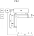
- FIG. 1 is a diagram illustrating an example of a display apparatus with an integrated antenna according to the present disclosure.
- the display apparatus with an integrated antenna includes a display panel 10 including a touch screen and an antenna electrode, a gate driver 200 transmitting a scan signal to gate lines GL1 to GLg provided in the display panel, a data driver 300 supplying data voltages to data lines DL1 to DLd provided in the display panel 10, a controller 400 controlling the gate driver 200 and the data driver 300, an antenna driver 700 transmitting an antenna signal transmitted from an external system to a wireless communication network via the antenna electrode or transmitting an antenna signal received from the antenna electrode to the external system, and a touch driver 600 driving the touch screen.
- the gate driver 200 generates scan signals using gate control signals GCS transmitted from the controller 400 and then supplies the scan signals to the gate lines GL1 to GLg.
- the gate driver 200 is formed independently of the display panel 10 and is connected to the display panel 10 through a tape carrier package (TCP), a chip-on film (COF), or a flexible printed circuit board (FPCB). However, the gate driver 200 may be formed directly in a non-display area of the display panel 10 using a gate in panel (GIP) method.
- TCP tape carrier package
- COF chip-on film
- FPCB flexible printed circuit board
- GIP gate in panel
- the data driver 300 converts image data transmitted from the controller 400 into data voltages and then supplies the data voltages to the data lines DL1 to DLd.
- the controller 400 generates a gate control signal GCS for controlling driving of the gate driver 200 and a data control signal DCS for controlling driving of the data driver 300 using a timing synchronization signal input from the external system 900. Further, the controller 400 converts input image data input from the external system 900 into image data and transmits the image data to the data driver 300.
- the antenna driver 700 transmits the antenna signal transmitted from the external system 900 to a wireless communication network through the antenna electrode provided in the display panel 10 or transmits the antenna signal received from the antenna electrode to the external system 900.
- the touch driver 600 determines whether the display panel 10 is touched using touch sensing signals received from the touch screen.
- a touch position of the display panel 10 may be determined by the touch driver 600 or may be determined by the controller 400 that receives information related to the touch from the touch driver 600.
- the display panel 10 is divided into a display area AA and a non-display area NAA surrounding the display area AA and includes a pixel array part 100 including pixel driving circuits and light emitting devices provided on the display area AA and an electrode array part 500 provided on the pixel array part 100 and including the touch screen and the antenna electrode.
- a pixel 110 including the pixel driving circuit and the light emitting device is provided, and a portion corresponding to the light emitting device of the touch screen is open.
- the display area AA is provided in an intermediate area of the display panel 10 and may be defined as an area for displaying an image.
- the display area AA may have a rectangular shape, a rectangular shape in which each corner portion has a predetermined radius of curvature, or a non-square shape having at least six sides, or may be formed in various shapes.
- the non-display area NAA surrounds the display area AA, and thus the shape of the non-display area NAA may be variously changed according to the shape of the display area AA.
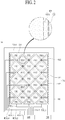
- FIG. 2 is a view showing a planar structure of a display panel applied to a display apparatus with an integrated antenna according to the present disclosure
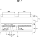
- FIG. 3 is a cross-sectional view taken along line A-A' of FIG. 2 . Since the line A-A' in FIG. 3 extends over two pixels, a cross-section of two pixels is shown in FIG. 3 .
- the display panel 10 applied to the display apparatus with an integrated antenna according to the present disclosure is divided into the display area AA and the non-display area NAA as shown in FIGS. 1 to 3 .
- the display panel 10 may be a panel including a light emitting device such as an organic light emitting diode, or a panel including liquid crystal.
- a light emitting device such as an organic light emitting diode
- a panel including liquid crystal a light emitting device including liquid crystal.
- a pixel 110 including the pixel driving circuit and the light emitting device ED is provided in the display area AA.
- the display panel 10 includes the substrate 102 including the display area AA and the non-display area NAA surrounding the display area AA, a pixel array layer 104 including the pixel driving circuits and the light emitting devices ED provided on the display area AA, an insulating layer 106 covering the pixel array layer 104, an antenna electrode 502 provided on the insulating layer 106, an encapsulation layer 504 provided on the antenna electrode 502, a touch screen TS provided on the encapsulation layer 504, and a passivation layer 524 covering the touch screen TS.
- the substrate 102 is a base substrate (or base layer) and includes a plastic material or a glass material.
- the pixel array layer 104 includes the pixel driving circuits and the light emitting devices (EDs).
- EDs light emitting devices
- the pixel driving circuit controls the amount of current flowing in the light emitting device ED based on a data voltage supplied from the data line DL in response to a scan signal supplied from one gate line GL.
- the pixel driving circuit may include two thin film transistors and one capacitor.
- the pixel driving circuit may include a driving transistor Tdr controlling the amount of current supplied to the light emitting device ED according to the data voltage, a switching transistor supplying the data voltage supplied from the data line DL to the driving transistor Tdr, and a capacitor storing a voltage between a gate and a source of the driving transistor Tdr.
- the pixel driving circuit may further include at least one transistor for sensing a characteristic change of the driving transistor Tdr or compensating for a change in characteristic of the driving transistor Tdr.
- the light emitting device ED emits light by a current supplied from the pixel driving circuit and emits light having a luminance corresponding to a magnitude of the current.
- the light emitting device ED includes a first electrode ED1 electrically connected to the driving transistor Tdr, a light emitting layer ED2 formed on the first electrode ED1, and a second electrode ED3 electrically connected to the light emitting layer ED2. That is, the light emitting device ED includes the first electrode ED1, the light emitting layer ED2 provided on the first electrode ED1, and the second electrode ED3 provided on the light emitting layer ED2.
- the light emitting layer ED2 may include any one of a blue light emitting portion, a green light emitting portion, and a red light emitting portion for emitting light having a color corresponding to a color set in the pixel 110.
- the light emitting layer ED2 may include any one of an organic light emitting layer, an inorganic light emitting layer, and a quantum dot light emitting layer, or may include a stacked or mixed structure of the organic light emitting layer (or the inorganic light emitting layer) and the quantum dot light emitting layer.
- the pixel array layer 104 may include the pixel driving circuits and the light emitting devices ED.
- the driving transistor Tdr which constitutes the pixel driving circuit
- the light emitting device ED connected to the driving transistor Tdr.
- the first electrode ED1 constituting the light emitting device ED is referred to as an anode
- the second electrode ED3 is referred to as a cathode.
- the cathode ED3 is provided on the entire surface of the display area AA of the display panel 10 as shown in FIG. 3 .
- the insulating layer 106 covers the pixel array layer 104, and particularly covers the cathode ED3.
- the insulating layer 106 may be formed of a dielectric.
- the insulating layer 106 may be formed of a material such as silicon nitride (SiNx) or silicon oxide (SiOx).
- the cathode ED3, the insulating layer 106, and the antenna electrode 502 form an antenna.
- the antenna electrode 502 is provided on the insulating layer 106.
- the antenna electrode 502 may be formed of a transparent conductive material, that is, a metal.
- the cathode ED3 connected to a ground, the antenna electrode 502 formed of a transparent conductive material, and the insulating layer 106 provided between the cathode ED3 and the antenna electrode 502 constitute the antenna, and the antenna serves to receive an antenna signal received through a wireless communication network or output an antenna signal transmitted from the antenna driver 700 to the wireless communication network.
- the antenna electrode 502 is provided on the top of the cathode ED3, the insulating layer 106 is provided between the cathode ED3 and the antenna electrode 502, and the cathode ED3 and the antenna electrode 502 form the antenna.
- the encapsulation layer 504 is provided on the antenna electrode 502.
- the encapsulation layer 504 may prevent oxygen or moisture from penetrating into the light emitting device ED provided in the pixel array layer 104.
- the encapsulation layer 504 may include at least one inorganic layer.
- the encapsulation layer 504 may include a plurality of inorganic layers and organic layers provided between the plurality of inorganic layers.
- the inorganic layer may serve to block penetration of water or oxygen and may be formed of an inorganic material such as silicon nitride, aluminum nitride, zirconium nitride, titanium nitride, hafnium nitride, tantalum nitride, silicon oxide, aluminum oxide, or titanium oxide, or the like.
- an inorganic material such as silicon nitride, aluminum nitride, zirconium nitride, titanium nitride, hafnium nitride, tantalum nitride, silicon oxide, aluminum oxide, or titanium oxide, or the like.
- the organic layer may be formed to have a relatively thicker than the inorganic layer so as to cover foreign objects that may occur during a manufacturing process.
- the organic layer may be formed of an organic material such as silicon oxycarbon (SiOCz) acryl or epoxy-based resin.
- the organic layer may be formed by a coating process, for example, an inkjet coating process or a slit coating process.
- the touch screen TS is provided on the encapsulation layer 504.
- the touch screen TS may be configured according to a self-capacitance method or according to a mutual-capacitance method.
- the touch driver 600 supplies a touch driving signal to each of electrode patterns EP constituting the touch screen TS and receives a touch sensing signal from each of the electrode patterns EP.
- the touch driver 600 sequentially applies a touch driving signal to each of the touch driving electrodes formed by the electrode patterns EP constituting the touch screen TS, and receives touch sensing signals respectively from the touch sensing electrodes formed by the electrode patterns EP constituting the touch screen TS.
- the electrode pattern EP may be formed in a rhombus shape within the display area AA and may be formed in a triangular shape in an area of the display area AA adjacent to the non-display area NAA.
- the shape of the electrode pattern EP may be variously changed.
- the electrode pattern EP may constitute the touch driving electrode or may constitute the touch sensing electrode in a touch screen configured according to the mutual-capacitance.
- the electrode pattern EP may be one independent touch electrode in a touch screen configured according to the self-capacitance method. In the following description of other drawings, the feature may be applied in the same scheme.
- a touch screen TS using the mutual-capacitance method will be described as an example of the present disclosure.
- the present disclosure may also be applied to a touch screen TS using the self-capacitance method.
- the passivation layer 524 covers the touch screen TS.
- the passivation layer 524 may be formed of an inorganic material, for example, silicon oxide (SiOx) or silicon nitride (SiNx).
- the touch screen TS and the antenna electrode 502 are provided on different layers, and the antenna electrode 502 is provided between the pixel array part 510 and the touch screen TS.
- a portion of the touch screen TS corresponding to the light emitting device ED is open.
- the open portion corresponding to the light emitting device is referred to as an open area OPA.
- the portion corresponding to the light emitting device ED is open.
- the portion of the touch screen TS corresponding to the light emitting device ED of the touch screen TS is open.
- the substrate 102, the pixel array layer 104, and the insulating layer 106 constitute the pixel array part 100, and the antenna electrode 502, the encapsulation layer 504, the touch screen TS, and the passivation layer 524 constitute the electrode array part 500.
- the display panel 10 includes the pixel array part 100 including the pixels 110 and the electrode array part 500 provided on the pixel array part 100 and including the touch screen TS and the antenna electrode 502.
- the electrode array part 500 may be divided into an antenna array part 510 and a touch array part 520.
- the electrode array part 500 includes the antenna array part 510 including the antenna electrode 502 and the touch array part 520 including the touch screen TS.
- the antenna array part 510 is provided on the pixel array part 100 and the touch array part 520 is provided on the antenna array part 510.
- the touch screen TS includes the electrode patterns EP as shown in FIG. 2 .
- each of the electrode patterns EP covers at least two pixels. Sizes of the electrode patterns EP may be variously set according to a touch object (finger or pen), touch sensitivity, the number of coordinates to be sensed, and the like.
- the portion of the touch screen TS corresponding to the light emitting device ED is open, and in particular, a portion of the electrode pattern EP corresponding to the light emitting devices EDs provided in the at least two pixels covered by the electrode pattern EP is open.
- the light emitting devices ED may be separated by a bank 108, and an electrode pattern line 522 constituting the electrode pattern EP is formed in an area corresponding to the bank 108, and an area of the electrode pattern EP corresponding to the light emitting device ED is an open area OPA. That is, one electrode pattern EP includes a plurality of open areas OPA and a plurality of electrode pattern lines 522 that distinguish between the open areas OPA as shown in FIG. 2 .
- the touch screen TS and the antenna electrode 502 are provided on different layers, and the antenna electrode 502 is provided between the pixel array part 100 and the touch screen TS.
- the antenna electrode 502 is provided in the portion of the touch screen TS corresponding to the light emitting device ED, that is, in the open area OPA.
- the antenna electrode 502 since the antenna electrode 502 is provided in the entirety of the display area AA of the display panel 10 in the form of a plate, the antenna electrode 502 may be provided in the open area OPA.
- the touch screen TS When the touch screen TS is configured using the mutual scheme, the touch screen TS includes driving electrodes and reception electrodes.
- the touch screen TS including three driving electrodes and four reception electrodes is shown as an example of the present disclosure.
- the number of the driving electrodes and the number of the reception electrodes may be variously set according to the size of the display panel 10 or the like.
- Each of the driving electrodes includes driving electrode patterns extending in a first direction of the display panel 10 among the electrode patterns EP.
- the driving electrode patterns constituting the first driving electrode are denoted by TX1
- the driving electrode patterns constituting the second driving electrode are denoted by TX2
- the driving electrode patterns constituting the third driving electrode are denoted by TX3.
- the first direction may be a lengthwise direction in FIG. 2 and may be parallel to the data line DL in FIG. 1 .
- the driving electrode patterns constituting the first driving electrode are electrically connected to each other by first driving electrode bridges
- the driving electrode patterns constituting the second driving electrode are electrically connected to each other by second driving electrode bridges
- the driving electrode patterns constituting the third driving electrode are electrically connected to each other by third driving electrode bridges.
- Each of the reception electrodes includes reception electrode patterns extending in a second direction different from the first direction among the electrode patterns EP.
- the reception electrode patterns constituting the first reception electrode are denoted by RX1
- the reception electrode patterns constituting the second reception electrode are denoted by RX2
- the reception electrode patterns constituting the third reception electrode are denoted by RX3
- the reception electrode patterns constituting the fourth reception electrode are denoted by RX4.
- the second direction may be a widthwise direction in FIG. 2 and may be parallel to the gate line GL in FIG. 1 .
- the reception electrode patterns constituting the first reception electrode are electrically connected to each other by the first reception electrode bridges
- the reception electrode patterns constituting the second reception electrode are electrically connected to each other by the second reception electrode bridges
- the reception electrode patterns constituting the third reception electrode are electrically connected to each other by the third reception electrode bridges
- the reception electrode patterns constituting the fourth reception electrode are electrically connected to each other by the fourth reception electrode bridges.
- the touch screen TS is shown as a single layer on the top of the encapsulation layer 504 in FIGS. 2 and 3
- the reception electrode patterns, the driving electrode patterns, the reception electrode bridges, and the driving electrode bridges may be configured as a plurality of layers including at least one insulating layer.
- the first driving electrode to the third driving electrode are connected to the touch driver 600 by first driving electrode line to third driving electrode line TXL1, TXL2, and TXL3, respectively, and the first reception electrode to the fourth reception electrode are connected to the touch driver 600 by the first reception electrode line to the fourth reception electrode line RXL1, RXL2, RXL3, and RXL4, respectively.
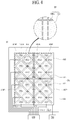
- FIGS. 4 to 6 are views showing another example of a planar structure of a display panel applied to the display apparatus with an integrated antenna according to the present disclosure.
- the same or similar contents as those described with reference to FIGS. 1 to 3 are omitted or briefly described.
- the display panel 10 includes the pixel array part including the pixels 110 and the electrode array part 500 provided on the pixel array part 100 and including the touch screen TS and the antenna electrode 502.
- the electrode array part 500 includes the antenna array part 510 provided on the pixel array part 100 and including the antenna electrode 502 and the touch array part 520 provided on the antenna array part 510 and including the touch screen TS.
- the touch screen TS and the antenna electrode 502 are provided on different layers and the antenna electrode is provided between the pixel array part 100 and the touch screen TS.
- the antenna electrode 502 may be formed in a single plate shape and may be provided on the entire surface of the display area AA as shown in FIG. 2 , and may include at least two antenna patterns ANP as shown in FIG. 6 .
- FIG. 4 illustrates an antenna electrode 502 including four antenna patterns ANP
- FIG. 5 illustrates an antenna electrode 502 including 16 antenna patterns ANP.
- FIG. 6 illustrates an antenna electrode 502 including antenna patterns ANP separated in the same form as the electrode patterns EP.
- the antenna patterns ANP may be formed in various shapes such as a square, a hexagon, an octagon, and a circle.
- the antenna patterns ANP may be electrically connected through antenna bridges ANB and connected to the antenna driver 700.
- the touch screen TS is driven by the touch driver 600, and the antenna electrode 502 is driven by the antenna driver 700.
- the touch driver 600 and the antenna driver 700 are independently driven. That is, the process of determining whether the display panel 10 is touched by the touch driver 600 is not affected by the process of outputting or receiving an antenna signal by the antenna driver 700 using the antenna electrode 502.
- the antenna is a passive element, an output compared with an input is reduced, and therefore it is necessary to secure an antenna gain through a low-resistance wiring.
- the characteristics of the antenna are affected not only by resistance but also by capacitance between a ground metal and the antenna electrode.
- a low dielectric constant material must be applied and the size of the antenna is also determined according to a magnitude of capacitance.
- the cathode ED3 provided on the entire surface of the display panel may be used as a ground electrode of the antenna, capacitance of the antenna may be increased, thereby improving performance of the antenna.
- the antenna electrode is divided into a plurality of antenna patterns, performance of the antenna may be improved.
- the antenna electrode 502 since the shape of the antenna electrode 502 does not affect the touch screen TS and other elements, the antenna electrode 502 may be divided into various types of antenna patterns ANP as shown in FIGS. 4 to 6 , and thus, performance of the antenna may be improved.
- the antenna of the above-described type applied to the present disclosure is referred to as a patch antenna.
- the patch antenna uses a method of supplying electricity through a rectangular or circular metal provided on a microstrip substrate.
- the microstrip substrate may correspond to the cathode ED3 in the present disclosure, and the metal may correspond to the antenna electrode 502.
- the patch antenna may be embedded in the display panel 10 together with the touch screen TS, and the performance of the patch antenna may be improved.
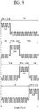
- FIG. 7 is a view illustrating another example of a planar structure of a display panel applied to a display apparatus with an integrated antenna according to the present disclosure
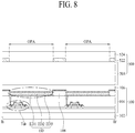
- FIG. 8 is a cross-sectional view taken along line B-B' of FIG. 7
- FIG. 9 is a view illustrating an operation method of a touch mode and an antenna mode according to an embodiment of the present disclosure
- FIG. 10 is a view illustrating another example of an operation method of a touch mode and an antenna mode applied to the present disclosure. Since the line B-B' in FIG. 7 extends over two pixels, the cross-section of the two pixels is shown in FIG. 8 .
- the same or similar contents as those described with reference to FIGS. 1 to 6 are omitted or briefly described.
- a display apparatus with an integrated antenna includes a display panel 10 including a touch screen and an antenna electrode, a gate driver 200 transmitting scan signals to gate lines GL1 to GLg provided in the display panel 10, a data driver 300 supplying data voltages to the data lines DL1 to DLd provided in the display panel 10, a controller 400 controlling the gate driver 200 and the data driver 300, an antenna driver 700 transmitting an antenna signal transmitted from an external system to a wireless communication network via the antenna electrode or transmitting an antenna signal received from the antenna electrode to the external system, and a touch driver 600 driving the touch screen.
- the display panel 10 includes array part 100 including the pixels 110 and the electrode array part 500 provided on the pixel array part 100 and including the touch screen and the antenna electrode.
- the display area includes a pixel including a pixel driving circuit and a light emitting device, and a portion of the touch screen corresponding to the light emitting device is open.
- the portion of the touch screen corresponding to the light emitting device ED is open.
- the open portion corresponding to the light emitting device is referred to as an open area OPA.
- the electrode array part 500 may be used as the touch screen or as the antenna.
- the entirety of the electrode array part 500 may be used as the touch screen or as the antenna.
- a portion of the electrode array part 500 corresponding to the light emitting device ED is open and a portion of the electrode patterns EP constituting the electrode array part 500 corresponding to the light emitting device ED provided in at least two pixels covered by the electrode pattern EP is open.
- the light emitting devices ED may be separated by the bank 108, an area corresponding to the bank 108 includes the electrode pattern line 522 constituting the electrode pattern EP, and an area of the electrode pattern EP corresponding to the light emitting device ED is the open area OPA.
- the electrode array part 500 includes an encapsulation layer 504 provided on the pixel array part, an electrode unit ELU provided on the encapsulation layer 504, and a passivation layer 524 covering the electrode unit ELU, and the electrode unit ELU is used as at least one of the touch screen and the antenna electrode.
- the light emitting device ED includes an anode electrode ED1, a light emitting layer ED2 provided on the anode electrode ED1, and a cathode ED3 provided on the light emitting layer ED2.
- the cathode ED3 is provided on the entire display area AA, and the electrode patterns EP included in the at least one antenna area and the cathode ED3 form an antenna.
- a difference of the present disclosure described with reference to FIGS. 7 and 8 is that, in the display panel 10 shown in FIGS. 7 and 8 , some of the electrode patterns EP is used as the touch screen and the other is used as the antenna electrode. In the display panel 10 shown in FIGS. 7 and 8 , all of the electrode patterns EP may be used as the touch screen or may be used as the antenna electrode.
- the electrode patterns EP are used only as the touch screen, the display panel 10 shown in FIGS. 7 and 8 , the electrode patterns EP may be used as the touch screen and the antenna electrode.
- the electrode patterns EP constitute the touch screen TS, but, in the description of FIGS. 7 to 10 , the electrode patterns EPs constitute the electrode unit ELU. That is, the electrode unit ELU may be used as the touch screen and the antenna electrode.
- the electrode unit ELU includes the electrode patterns EP and the electrode patterns EP include external patterns RX1_1, RX1_2, RX2_1, RX2_2, RX3_1, RX3_2, RX4_1, RX4_2, TX1_1, TX1_2, TX2_1, TX2_2, TX3_1, and TX3_2 adjacent to the non-display area NAA and internal patterns TX1, TX2, TX3, RX1, RX2, RX3, and RX4 surrounded by the external patterns.
- the external patterns are used as the touch screen in the touch mode and as the antenna electrode in the antenna mode.
- the internal patterns may also be used as the antenna electrode in the antenna mode.
- a display panel in which only the external patterns are used as the touch screen or the antenna electrode will be described as an example of the present disclosure.
- the external patterns may be divided into at least two antenna areas.
- external patterns constituting any one of the at least two antenna areas are used as the antenna electrode, and external patterns constituting the remaining antenna area may be used as the touch screen.
- the external patterns constituting the remaining antenna area of the at least two antenna areas are used as the antenna electrode, and the external patterns that constitute the any one antenna area may be used as the touch screen.
- the external patterns may be divided into at least two antenna areas, and the antenna areas may alternately be used as an antenna electrode.
- FIG. 7 shows the display panel 10 in which the external patterns are divided into four antenna areas as an example of the present disclosure.
- the external patterns RX1_1, RX2_1, RX3_1, and RX4_1 provided on a first side of the display area AA may form a first antenna group 1GR
- external patterns RX1_2, RX2_2, RX3_2 and RX4_2 provided on a second side of the display area AA facing the first side may form a second antenna group 2GR
- external patterns TX1_1, TX2_1, and TX3_1 provided between the first side and the second side of the display area AA may form a third antenna group 3GR
- external patterns TX1_2, TX2_2, and TX3_2 provided on a fourth side of the display area AA facing the third side may form a fourth antenna group 4GR.
- the first side may refer to a left side of the display panel shown in FIG. 7
- the second side may refer to a right side of the display panel
- the third side may refer to the top of the display panel
- the fourth side may refer to the bottom of the display panel.
- the touch driver 700 uses all of the electrode patterns as the touch screen in the touch mode TM and connects at least one of the first to fourth antenna groups 1GR to 4GR to the antenna driver 700 in the antenna mode AM. That is, in the touch mode TM, all the electrode patterns EP are used as the touch screen, and in the antenna mode AM, electrode patterns EP included in at least one of the first to fourth antenna groups 1GR to 4GR may be used as the antenna electrode.
- the external patterns constituting the first antenna group 1GR are used as the antenna electrode
- the external patterns constituting the second antenna group 2GR are used as the antenna electrode
- the external patterns constituting the third group 3GR are used as the antenna electrode
- the external patterns constituting the fourth group 4GR are used as the antenna electrode.
- each of the first to fourth groups 1GR to 4GR is used as an antenna electrode, that is, in the first antenna mode AM, the second antenna mode AM, the third antenna mode AM, and the fourth antenna mode AM, the remaining antenna patterns are not driven.
- an antenna function is performed by at least one of the first to fourth groups 1GR to 4GR and the touch function is not performed.
- the touch mode TM all the electrode patterns EP are used as a touch screen.
- a plurality of touch driving signals are supplied to the electrode patterns EP, so that a touch may be detected.
- the antenna mode AM may be concurrent with the touch mode TM.
- the touch mode TM for touch sensing may occur in all the periods of one frame period, and the antenna mode AM for transmitting and receiving an antenna signal may occur in a part of one frame period.
- transmission and reception of the antenna signal may be performed using signals having an amplitude larger than the touch driving signals, as shown in FIG. 10 . That is, in order to prevent interference between the antenna signal and the touch driving signal, the antenna signal may have an amplitude larger than the touch driving signal.
- touch sensing may be continuously performed, and the antenna signal may be transmitted and received only during a part of one frame period.
- electrode patterns EP included in at least one of the first to fourth antenna groups 1GR to 4GR may be used as the antenna electrode in a part of the one frame period.
- the antenna mode AM may also continuously occur substantially in the one frame period. Therefore, the transmitting and receiving function of the antenna signal may be improved.
- the internal patterns TX1, TX2, TX3, RX1, RX2, RX3, and RX4 may be used as a touch screen during one frame period. Therefore, whether the display panel 10 is touched may be continuously determined during the one frame period.
- only the first antenna group 1GR among the first to fourth antenna groups 1GR to 4GR may be used as the antenna electrode during a 1/4 of one frame period
- only the second antenna group 2GR may be used as the antenna electrode during another 1/4 period
- only the third antenna group 3RG may be used as the antenna electrode during another 1/4 period
- only the fourth antenna group 4RG may be used as the antenna electrode during the remaining 1/4 period.
- all of the first to fourth antenna groups 1GR to 4GR may be used as the antenna electrode.
- all of the external patterns since all of the external patterns are used as antenna electrode, touch sensitivity of the touch screen may be reduced. Therefore, in the display panel that does not require high touch sensitivity, all of the external patterns may be used as the antenna electrode during a part of one frame period.
- the antenna groups may be set in various numbers and types, and the number and positions of antenna groups driven in the antenna mode may also be variously set.
- a display panel in which only the external patterns are used as the touch screen or the antenna electrode, the external patterns are divided into first to fourth antenna groups 1GR to 4GR as illustrated in FIG. 7 , and the first to fourth antenna groups 1GR to 4GR operate in the form shown in FIG. 10 will be described as an example of the present disclosure.
- the touch driver 600 includes a driving signal supply part 610 sequentially transmitting touch driving signals to the driving electrodes and a touch sensing part 620 receiving a touch sensing signal from the reception electrodes and determining whether a touch is applied.
- Each of the driving electrodes includes driving electrode patterns extending in the first direction of the display panel 10 among the electrode patterns EP.
- driving electrode patterns constituting the first driving electrode are denoted by TX1
- driving electrode patterns constituting the second driving electrode are denoted by TX2
- driving electrode patterns constituting the third driving electrode are denoted by TX3.
- the driving electrode patterns constituting the first driving electrode are electrically connected to each other by the first driving electrode bridges
- the driving electrode patterns constituting the second driving electrode are electrically connected to each other by the second driving electrode bridges
- the driving electrode patterns constituting the third driving electrode are electrically connected to each other by the third driving electrode bridges.
- a driving electrode pattern TX1_1 provided on the third side among the driving electrode patterns constituting the first driving electrode, a driving electrode pattern TX2_1 provided on the third side among the driving electrode patterns constituting the second driving electrode, and a driving electrode pattern TX3_1 provided on the third side among the driving electrode patterns constituting the third driving electrode are external patterns included in the third antenna group 3RG.
- a driving electrode pattern TX1_2 provided on the fourth side among the driving electrode patterns constituting the first driving electrode, a driving electrode pattern TX2_2 provided on the fourth side among the driving electrode patterns constituting the second driving electrode, and a driving electrode pattern TX3_2 provided on the fourth side among the driving electrode patterns constituting the third driving electrode are external patterns included in the fourth antenna group 3RG.
- Driving electrode patterns excluding the two external patterns provided on the third side and the fourth side among the driving electrode patterns constituting the first driving electrode are internal patterns
- driving electrode patterns excluding the two external patterns provided on the third side and the fourth side among the driving electrode patterns constituting the second driving electrode are internal patterns
- driving electrode patterns excluding the two external patterns provided on the third side and the fourth side among the driving electrode patterns constituting the third driving electrode are internal patterns.
- the internal patterns among the driving electrode patterns constituting the first driving electrode are connected to the driving signal supply part 610 through the first internal pattern line TL1
- the external pattern provided on the third side is connected to the driving signal supply part 610 through the (1_1)th external pattern line TL1_1 provided on the third side
- the external pattern provided on the fourth side is connected to the driving signal supply part 610 through the (1_2)th external pattern line TL1_2.
- the driving electrode patterns constituting the second driving electrode are also connected to the driving signal supply part 610 through the second internal pattern line TL2, the (2_1)th external pattern line TL2_1, and the (2_2)th external pattern line TL2_2.
- the driving electrode patterns constituting the third driving electrode are also connected to the driving signal supply part 610 through the third internal pattern line TL3, the (3_1)th external pattern line TL3_1, and the (3_2)th external pattern line TL3_2.
- Each of the reception electrodes includes reception electrode patterns extending in the second direction different from the first direction among the electrode patterns EP.
- the reception electrode patterns constituting the first reception electrode are denoted by RX1
- the reception electrode patterns constituting the second reception electrode are denoted by RX2
- the reception electrode patterns constituting the third reception electrode are denoted by RX3
- the reception electrode patterns constituting the fourth reception electrode are denoted by RX4.
- the reception electrode patterns constituting the first reception electrode are electrically connected to each other by first reception electrode bridges
- the reception electrode patterns constituting the second reception electrode are electrically connected to each other by second reception electrode bridges
- the reception electrode patterns constituting the third reception electrode are electrically connected to each other by the third reception electrode bridges
- the reception electrode patterns constituting the fourth reception electrode are electrically connected to each other by the fourth reception electrode bridges.
- Each of the first to fourth reception electrodes may be classified into internal patterns and external patterns similarly to the first to third driving electrodes.
- the internal patterns among the reception electrode patterns constituting the first reception electrode are connected to the touch sensing part 620 through the first internal pattern line RL1, the external pattern provided on the first side is connected to the touch sensing part 620 through the (1_1)th external pattern line RL1_1, and the external pattern provided on the second side is connected to the touch sensing part 620 through the (1_2)th external pattern line RL1_2.
- the reception electrode patterns constituting the second reception electrode are also connected to the touch sensing part 620 through the second internal pattern line RL2, the (2_1)th external pattern line RL2_1. and the (2_2)th external pattern line RL2_2.
- the reception electrode patterns constituting the third reception electrode are also connected to the touch sensing part 620 through the third internal pattern line RL3, the (3_1)th external pattern line RL3_1, and the (3_2)th external pattern line RL3_2.
- the reception electrode patterns constituting the fourth reception electrode are also connected to the touch sensing part 620 through the fourth internal pattern line RL4, the (4_1)th external pattern line RL4_1, and the (4_2)th external pattern line RL4_2.
- a touch driving signal is sequentially supplied to the first to third driving electrodes. That is, after the touch driving signal is supplied to the first driving electrode in the touch mode, the touch driving signal is supplied to the second driving electrode, and finally, the touch driving signal is supplied to the third driving electrode.
- the driving signal supply part 610 includes a first driving switch 612 for sequentially supplying the touch driving signal to the first to third driving electrodes, a second driving switch 613 for connecting the external patterns constituting the first to third driving electrodes to the antenna driver 700, and a touch driving signal generating unit 611 for outputting the touch driving signal to the first driving switch 612.
- a touch synchronization signal TSS for controlling the first driving switch 612 may be generated by the touch driving signal generating unit 611 or may be transmitted from the controller 400.
- An antenna synchronization signal ASS for controlling the second driving switch 613 may be generated by the touch driving signal generating unit 611 or may be transmitted from the controller 400.
- the first driving switch 612 connects one of the first to third driving electrodes to the touch drive signal generating unit 611 as shown in FIG. 7 .
- the second driving switches 613 connect the (1_1)th external pattern line TL1_1, the (1_2)th external pattern line TL1_2, the (2_1)th external pattern line TL2_1, the (2_2)th external pattern line TL2_2, the (3_1)th external pattern line TL3_1, and the (3_2)th external pattern line TL3_2 connected to the driving electrodes to the antenna driver 700 or to the first driving switch 612.
- the second driving switches 613 connect the lines to the first driving switch 612.
- the first driving switch 612 sequentially supplies the touch driving signal to the driving electrodes by the touch synchronization signal TSS.
- the touch driving signal may be sequentially supplied to the first to third driving electrodes.
- the second driving switches 613 connect the lines to the antenna driver 700.
- the second driving switches 613 connected to the same antenna group among the second driving switches 613 are simultaneously connected to the antenna driver 700, and the second driving switches 613, are sequentially connected to the antenna driver 700.
- the antenna groups may sequentially perform the function of the antenna electrode.
- the first to fourth reception electrodes are connected to the touch sensing part 620.
- the external patterns constituting the first to fourth reception electrodes must be connected to the antenna driver 700.
- the touch sensing part 620 includes sensing switches 622 for connecting the external patterns constituting the first to fourth reception electrodes to the antenna driver 700 and a touch determining unit 621 receiving touch sensing signals from the first to fourth reception electrodes and determining whether the display panel 10 is touched.
- the antenna synchronization signal ASS for controlling the sensing switches 622 may be generated by the touch determining unit 621 or may be transmitted from the controller 400.
- the antenna synchronization signal ASS for controlling the sensing switches 622 may be the same signal as the antenna synchronization signal ASS for controlling the second driving switches 613.
- the sensing switches 622 connect the lines connected to the first to fourth reception electrodes to the touch determining unit 621.
- the touch determining unit 621 determines whether the display panel 10 is touched using the touch sensing signals received from the first to fourth reception electrodes.
- the sensing switches 622 connect the lines connected to the external patterns constituting the first to fourth reception electrodes to the antenna driver 700.
- the sensing switches 622 connected to the same antenna group among the sensing switches 622 are simultaneously connected to the antenna driver 700, and the sensing switches 622 connected to different antenna groups are sequentially connected to the antenna driver 700.
- the antenna groups may sequentially perform the function of the antenna electrode.
- one antenna group may include external patterns connected to the reception electrodes and external patterns connected to the driving electrodes.
- the external patterns included in one antenna group must be connected to the antenna driver 700 at the same time.
- the antenna synchronization signal ASS for controlling the sensing switches 622 may be the same signal as the antenna synchronization signal ASS for controlling the second driving switches 613.
- the electrode unit ELU is driven in a time division manner so that the electrode unit ELU may be used as a touch screen and an antenna electrode.
- an antenna signal may be transmitted and received even while it is determined whether the touch is applied.
- the antenna signal may be radiated to the front surface of the display panel 10 or an antenna signal may be received from the front surface of the display panel 10.
- the transmission/reception efficiency of the antenna may be increased.
- the touch driving signal generating unit 611 may be configured not to output the touch driving signal in the antenna mode AM when at least one of the first to fourth antenna groups 1GR to 4GR is used as an antenna electrode and if the remaining electrode patterns EP are not driven.
- FIG. 11 is a view showing another example of a planar structure of a display panel applied to a display apparatus with an integrated antenna according to the present disclosure.
- the same or similar contents as those described with reference to FIGS. 1 to 10 are omitted or briefly described.
- the electrode pattern EP may be formed in a rhombus shape within the display area AA as shown in FIG. 11 and may be formed in a triangular shape in the area of the display area AA adjacent to the non-display area NAA. Also, as shown in FIG. 11 , the electrode pattern EP may be used as one independent touch electrode in a touch screen configured according to the self-capacitance method. In addition, one electrode pattern EP includes a plurality of open areas OPA and a plurality of electrode pattern lines 522 demarcating the open areas OPA as shown in FIG. 11 .
- the touch screen applied to the display apparatus with an integrated antenna may be configured according to the mutual-capacitance method as shown in FIG. 7 or may be configured in the self-capacitance manner as shown in FIG. 11 .
- Each of the electrode patterns EP illustrated in FIG. 11 is denoted by reference numerals such as EP1_1, EP2_1, EP3_1, EP4_1, EP5, or the like.
- reference numerals such as EP1_1, EP2_1, EP3_1, EP4_1, EP5, or the like.
- reference numerals as shown in FIG. 11 are used. And in a case where the electrode patterns EP need not be separately described, reference numeral EP is used.
- the electrode patterns EP shown in FIG. 11 are separated from each other independently, unlike the electrode patterns EP shown in FIG. 7 . That is, the electrode patterns EP shown in FIG. 11 are formed to have the same structure as the electrode patterns EP shown in FIG. 7 , except that they are separated from each other. Therefore, in the following description, the features of the self-capacitance scheme will be described based on the contents described in FIG. 7 .
- the external patterns EP1_1, EP1_2, EP1_3, and EP1_4 included in the first antenna group 1GR are connected to a first antenna part 711 or a first touch part 651 through a first switching unit 810
- the external patterns EP2_1, EP2_2, EP2_3, and EP2_4 included in the second antenna group 2GR are connected to a second antenna part 712 or a second touch part 652 through a second switching unit 820
- the external patterns EP3_1, EP3_2, and EP3_3 included in the third antenna group 3GR are connected to a third antenna part 713 or a third touch part 653 through a third switching unit 830
- the external patterns EP4_1, EP4_2, and EP4_3 included in the fourth antenna group 4GR are connected to a fourth antenna part 714 or a fourth touch part 654 through a fourth switching unit 840
- the internal patterns EP5 are connected to a fifth touch part 655.
- the first to fourth antenna units 711 to 714 constitute the antenna driver 700 and the first to fifth touch parts 651 to 655 constitute the touch driver 600.
- the first to fourth switching units 810 to 840 connect the first to fourth antenna groups 1GR to 4GR to the touch driver 600.
- the touch driver 600 supplies a touch driving signal to each of the electrode patterns EP, and then, determines whether the display panel 10 is touched using the touch sensing signals received from each of the electrode patterns EP.
- each of the external patterns and each of the internal patterns receives the touch driving signal individually, and each of the touch sensing signals generated by each of the external patterns and each of the internal patterns is also transmitted to the touch driver 600 individually through the first to fifth touch parts 651 to 655.
- the touch driver 600 determines whether each of the external patterns and the internal patterns is touched using the touch sensing signals.
- the first to fourth switching units 810 to 840 connect at least one of the first to fourth antenna groups 1GR to 4GR to the antenna driver 700.
- the antenna driver 700 may transmit an antenna signal transmitted from the external system 900 to the wireless communication network through at least one of the first to fourth antenna groups 1GR to 4GR or transmit an antenna signal received through at least one of the first to fourth antenna groups 1GR to 4GR to the external system 900.
- the touch driver 600 may not output a touch driving signal.
- the antenna mode AM and the touch mode TM may be independently generated as described above with reference to FIG. 9 .
- the antenna mode AM may be generated together with the touch mode TM as described with reference to FIG. 10 .
- the first to fourth switching units 810 to 840 may connect at least one of the first to fourth antenna groups 1GR to 4GR to the antenna driver 700 and connect the remaining groups to the touch driver 600 in the antenna mode AM. Accordingly, in the antenna mode AM, the touch driving signal may be supplied to the other remaining electrode patterns EP, excluding the electrode patterns included in the antenna group connected to the antenna driver 700.
- the function of transmitting and receiving the antenna signal and the function of sensing the touch may be performed at the same time.
- the antenna since the antenna may be embedded in the display area of the display panel, a narrow bezel may be realized.
- the cathode of the light emitting device may be used as a ground electrode of the antenna, the characteristics of the antenna may be improved as compared with the related art.
- the word 'open' is used to mean that light and signals to/from the antenna may enter/leave the display device. In the particular implementations disclosed, this is achieved by providing gaps between the electrode pattern lines, but the skilled person will appreciate other ways of achieving this.
Landscapes
- Engineering & Computer Science (AREA)
- Theoretical Computer Science (AREA)
- General Engineering & Computer Science (AREA)
- Human Computer Interaction (AREA)
- Physics & Mathematics (AREA)
- General Physics & Mathematics (AREA)
- Computer Networks & Wireless Communication (AREA)
- Computer Hardware Design (AREA)
- Devices For Indicating Variable Information By Combining Individual Elements (AREA)
- Position Input By Displaying (AREA)
- Control Of El Displays (AREA)
- Electroluminescent Light Sources (AREA)
- Support Of Aerials (AREA)
- Details Of Aerials (AREA)
Applications Claiming Priority (1)
| Application Number | Priority Date | Filing Date | Title |
|---|---|---|---|
| KR1020180173502A KR102671154B1 (ko) | 2018-12-31 | 2018-12-31 | 안테나 일체형 표시장치 |
Publications (2)
| Publication Number | Publication Date |
|---|---|
| EP3674862A2 true EP3674862A2 (de) | 2020-07-01 |
| EP3674862A3 EP3674862A3 (de) | 2020-09-09 |
Family
ID=69005293
Family Applications (1)
| Application Number | Title | Priority Date | Filing Date |
|---|---|---|---|
| EP19218791.2A Pending EP3674862A3 (de) | 2018-12-31 | 2019-12-20 | Anzeigevorrichtung mit integrierter antenne |
Country Status (4)
| Country | Link |
|---|---|
| US (1) | US11175759B2 (de) |
| EP (1) | EP3674862A3 (de) |
| KR (1) | KR102671154B1 (de) |
| CN (1) | CN111381712B (de) |
Cited By (1)
| Publication number | Priority date | Publication date | Assignee | Title |
|---|---|---|---|---|
| CN114203060A (zh) * | 2020-09-18 | 2022-03-18 | 北京小米移动软件有限公司 | Micro LED显示面板和电子设备 |
Families Citing this family (23)
| Publication number | Priority date | Publication date | Assignee | Title |
|---|---|---|---|---|
| KR102089458B1 (ko) * | 2019-02-21 | 2020-03-16 | 동우 화인켐 주식회사 | 터치 센서 및 안테나를 포함하는 화상 표시 장치 |
| KR102099830B1 (ko) * | 2019-06-17 | 2020-04-10 | 동우 화인켐 주식회사 | 안테나 결합 모듈 및 이를 포함하는 디스플레이 장치 |
| KR102806193B1 (ko) * | 2019-09-10 | 2025-05-13 | 삼성전자주식회사 | 무선 충전 기능을 제공하는 전자 장치 및 그의 동작 방법 |
| KR102915058B1 (ko) * | 2019-10-08 | 2026-01-21 | 삼성디스플레이 주식회사 | 표시 장치 |
| US11016542B1 (en) * | 2020-02-25 | 2021-05-25 | Facebook, Inc. | Touch pad sensors operative as antennas |
| KR102913520B1 (ko) * | 2020-08-11 | 2026-01-15 | 동우 화인켐 주식회사 | 안테나 삽입 전극 구조체 및 이를 포함하는 화상 표시 장치 |
| TWI779339B (zh) * | 2020-08-25 | 2022-10-01 | 香港商南京矽力微電子(香港)有限公司 | 無線電子標籤及其系統 |
| CN112181200B (zh) * | 2020-09-28 | 2024-05-28 | 业成科技(成都)有限公司 | 触控显示模组以及触控显示装置 |
| KR102878665B1 (ko) * | 2020-12-16 | 2025-11-03 | 삼성디스플레이 주식회사 | 전자 장치 |
| CN112612374B (zh) * | 2020-12-28 | 2025-01-10 | 维沃移动通信有限公司 | 显示模组和电子设备 |
| CN112863350B (zh) * | 2021-01-19 | 2023-01-10 | 京东方科技集团股份有限公司 | 显示屏及显示终端 |
| KR102419269B1 (ko) * | 2021-01-20 | 2022-07-08 | 동우 화인켐 주식회사 | 안테나 어레이, 이를 포함하는 안테나 장치 및 디스플레이 장치 |
| US11172060B1 (en) * | 2021-02-13 | 2021-11-09 | Motorola Mobility Llc | Communication device having antenna tuning based on hand position detected by edge display |
| KR20230040625A (ko) | 2021-09-16 | 2023-03-23 | 삼성전자주식회사 | 안테나를 포함하는 전자 장치 |
| US20240381702A1 (en) * | 2021-09-24 | 2024-11-14 | Semiconductor Energy Laboratory Co., Ltd. | Display apparatus |
| CN114553993B (zh) * | 2021-12-27 | 2025-07-15 | 云谷(固安)科技有限公司 | 显示面板及显示装置 |
| CN114335985A (zh) * | 2021-12-29 | 2022-04-12 | 云谷(固安)科技有限公司 | 一种显示面板及显示模组 |
| CN114327146B (zh) * | 2021-12-31 | 2023-10-20 | 云谷(固安)科技有限公司 | 显示面板和显示装置 |
| CN114530694B (zh) * | 2022-04-24 | 2022-07-05 | 云谷(固安)科技有限公司 | 无线通信结构、显示面板和无线通信装置 |
| US12148982B2 (en) | 2022-05-16 | 2024-11-19 | Meta Platforms Technologies, Llc | Touch sensor and integrated antenna integrated film |
| KR20240000929A (ko) * | 2022-06-24 | 2024-01-03 | 동우 화인켐 주식회사 | 안테나 구조체 및 이를 포함하는 화상 표시 장치 |
| US12487494B2 (en) | 2022-08-26 | 2025-12-02 | Beijing Boe Optoelectronics Technology Co., Ltd. | Display substrate, manufacturing method thereof and display device |
| CN117940840A (zh) | 2022-08-26 | 2024-04-26 | 京东方科技集团股份有限公司 | 显示基板及其制备方法、显示装置 |
Family Cites Families (20)
| Publication number | Priority date | Publication date | Assignee | Title |
|---|---|---|---|---|
| EP1079296A2 (de) | 1999-08-06 | 2001-02-28 | Lucent Technologies Inc. | Elektronisch steuerbarer Antennenarray, der in einem tragbaren Rechner eingebettet ist |
| US6529096B2 (en) * | 2000-05-30 | 2003-03-04 | Matsushita Electric Industrial Co., Ltd. | Dielectric filter, antenna duplexer, and communications appliance |
| KR101177603B1 (ko) | 2005-07-04 | 2012-08-27 | 텔레폰악티에볼라겟엘엠에릭슨(펍) | 일체형 안테나를 갖는 일렉트로닉스 장치 |
| JP2010034617A (ja) * | 2008-07-24 | 2010-02-12 | Sony Corp | 通信装置 |
| JP2011138403A (ja) * | 2009-12-28 | 2011-07-14 | Sony Corp | 情報処理装置 |
| US20120034888A1 (en) | 2010-08-05 | 2012-02-09 | Franco De Flaviis | Method and System for Utilizing a Touchscreen Interface as an Antenna |
| KR102248849B1 (ko) | 2014-03-05 | 2021-05-07 | 삼성전자주식회사 | 안테나 장치 및 그를 구비하는 전자 장치 |
| CN103944614B (zh) * | 2014-03-21 | 2017-01-11 | 深圳市汇顶科技股份有限公司 | 近场通信系统和终端 |
| KR102139217B1 (ko) | 2014-09-25 | 2020-07-29 | 삼성전자주식회사 | 안테나 장치 |
| US20160188092A1 (en) * | 2014-12-22 | 2016-06-30 | Paneratech, Inc. | Touchscreen antenna system and design method thereof |
| KR102429283B1 (ko) | 2015-05-27 | 2022-08-05 | 삼성전자주식회사 | 디스플레이 장치 |
| CN105529539B (zh) | 2016-01-26 | 2018-06-05 | 广东欧珀移动通信有限公司 | 一种天线阵列及移动终端 |
| KR102499120B1 (ko) * | 2016-02-17 | 2023-02-15 | 삼성전자주식회사 | 안테나를 포함하는 전자 장치 |
| KR102469566B1 (ko) | 2016-03-31 | 2022-11-22 | 삼성전자주식회사 | 안테나 장치를 포함하는 전자 장치 |
| KR102334098B1 (ko) | 2016-04-20 | 2021-12-03 | 삼성전자주식회사 | 디스플레이가 포함된 전자 장치 |
| KR102666192B1 (ko) * | 2016-07-28 | 2024-05-14 | 삼성디스플레이 주식회사 | 표시 장치 |
| KR102737612B1 (ko) * | 2017-01-03 | 2024-12-05 | 삼성전자 주식회사 | 터치 정확도 향상을 위한 터치 센서의 배치 방법 및 상기 방법을 이용한 전자 장치 |
| KR102096417B1 (ko) | 2017-02-28 | 2020-04-02 | 동우 화인켐 주식회사 | 필름 타입의 마이크로스트립 패치 안테나 |
| US10732764B1 (en) * | 2018-09-05 | 2020-08-04 | Amazon Technologies, Inc. | Integrated touch control electrode and antenna |
| KR102190667B1 (ko) * | 2018-10-05 | 2020-12-14 | 동우 화인켐 주식회사 | 터치 센서-안테나 모듈 및 이를 포함하는 디스플레이 장치 |
-
2018
- 2018-12-31 KR KR1020180173502A patent/KR102671154B1/ko active Active
-
2019
- 2019-11-27 CN CN201911184189.3A patent/CN111381712B/zh active Active
- 2019-12-13 US US16/714,438 patent/US11175759B2/en active Active
- 2019-12-20 EP EP19218791.2A patent/EP3674862A3/de active Pending
Cited By (1)
| Publication number | Priority date | Publication date | Assignee | Title |
|---|---|---|---|---|
| CN114203060A (zh) * | 2020-09-18 | 2022-03-18 | 北京小米移动软件有限公司 | Micro LED显示面板和电子设备 |
Also Published As
| Publication number | Publication date |
|---|---|
| CN111381712B (zh) | 2023-06-06 |
| EP3674862A3 (de) | 2020-09-09 |
| KR102671154B1 (ko) | 2024-05-30 |
| US11175759B2 (en) | 2021-11-16 |
| US20200209995A1 (en) | 2020-07-02 |
| KR20200082674A (ko) | 2020-07-08 |
| CN111381712A (zh) | 2020-07-07 |
Similar Documents
| Publication | Publication Date | Title |
|---|---|---|
| EP3674862A2 (de) | Anzeigevorrichtung mit integrierter antenne | |
| US20240220042A1 (en) | Display device including touch screen function | |
| US10754461B2 (en) | Display device with integrated touch screen | |
| US11086158B2 (en) | Array substrate, display panel and man-machine interactive terminal | |
| US10936098B2 (en) | Display apparatus with integrated touch screen | |
| KR102601818B1 (ko) | 터치 센서를 구비하는 표시장치 | |
| US10996778B2 (en) | Display apparatus with integrated touch screen and method for fabricating the same | |
| US20140110683A1 (en) | Organic light emitting diode touch display panel | |
| US12353099B2 (en) | Display device | |
| KR20220075519A (ko) | 터치 디스플레이 장치 | |
| EP3457267B1 (de) | Eingabeerfassungsvorrichtung und anzeigemodul damit | |
| KR20170080314A (ko) | 터치패널이 내장된 표시장치 | |
| KR20240092665A (ko) | 터치 감지 장치 및 그를 포함하는 표시 장치 | |
| KR20230065760A (ko) | 터치 디스플레이 장치 및 디스플레이 패널 | |
| US20240423038A1 (en) | Display device | |
| US9678588B2 (en) | Wire-bonded borderless display | |
| US12455645B2 (en) | Touch display device | |
| US12547272B2 (en) | Sensor device and driving method thereof | |
| KR20250073794A (ko) | 터치 디스플레이 장치 및 디스플레이 패널 |
Legal Events
| Date | Code | Title | Description |
|---|---|---|---|
| PUAI | Public reference made under article 153(3) epc to a published international application that has entered the european phase |
Free format text: ORIGINAL CODE: 0009012 |
|
| STAA | Information on the status of an ep patent application or granted ep patent |
Free format text: STATUS: REQUEST FOR EXAMINATION WAS MADE |
|
| 17P | Request for examination filed |
Effective date: 20191220 |
|
| AK | Designated contracting states |
Kind code of ref document: A2 Designated state(s): AL AT BE BG CH CY CZ DE DK EE ES FI FR GB GR HR HU IE IS IT LI LT LU LV MC MK MT NL NO PL PT RO RS SE SI SK SM TR |
|
| AX | Request for extension of the european patent |
Extension state: BA ME |
|
| PUAL | Search report despatched |
Free format text: ORIGINAL CODE: 0009013 |
|
| AK | Designated contracting states |
Kind code of ref document: A3 Designated state(s): AL AT BE BG CH CY CZ DE DK EE ES FI FR GB GR HR HU IE IS IT LI LT LU LV MC MK MT NL NO PL PT RO RS SE SI SK SM TR |
|
| AX | Request for extension of the european patent |
Extension state: BA ME |
|
| RIC1 | Information provided on ipc code assigned before grant |
Ipc: G06F 3/044 20060101ALI20200805BHEP Ipc: G06F 3/041 20060101AFI20200805BHEP |
|
| RBV | Designated contracting states (corrected) |
Designated state(s): AL AT BE BG CH CY CZ DE DK EE ES FI FR GB GR HR HU IE IS IT LI LT LU LV MC MK MT NL NO PL PT RO RS SE SI SK SM TR |