EP3674863A1 - Verfahren zur herstellung einer berührungssteuerungsstruktur und berührungssteuerungsstruktur - Google Patents
Verfahren zur herstellung einer berührungssteuerungsstruktur und berührungssteuerungsstruktur Download PDFInfo
- Publication number
- EP3674863A1 EP3674863A1 EP18788994.4A EP18788994A EP3674863A1 EP 3674863 A1 EP3674863 A1 EP 3674863A1 EP 18788994 A EP18788994 A EP 18788994A EP 3674863 A1 EP3674863 A1 EP 3674863A1
- Authority
- EP
- European Patent Office
- Prior art keywords
- conductive layer
- pattern
- layer pattern
- touch structure
- manufacturing
- Prior art date
- Legal status (The legal status is an assumption and is not a legal conclusion. Google has not performed a legal analysis and makes no representation as to the accuracy of the status listed.)
- Withdrawn
Links
Images





Classifications
-
- G—PHYSICS
- G06—COMPUTING OR CALCULATING; COUNTING
- G06F—ELECTRIC DIGITAL DATA PROCESSING
- G06F3/00—Input arrangements for transferring data to be processed into a form capable of being handled by the computer; Output arrangements for transferring data from processing unit to output unit, e.g. interface arrangements
- G06F3/01—Input arrangements or combined input and output arrangements for interaction between user and computer
- G06F3/03—Arrangements for converting the position or the displacement of a member into a coded form
- G06F3/041—Digitisers, e.g. for touch screens or touch pads, characterised by the transducing means
- G06F3/044—Digitisers, e.g. for touch screens or touch pads, characterised by the transducing means by capacitive means
-
- G—PHYSICS
- G06—COMPUTING OR CALCULATING; COUNTING
- G06F—ELECTRIC DIGITAL DATA PROCESSING
- G06F3/00—Input arrangements for transferring data to be processed into a form capable of being handled by the computer; Output arrangements for transferring data from processing unit to output unit, e.g. interface arrangements
- G06F3/01—Input arrangements or combined input and output arrangements for interaction between user and computer
- G06F3/03—Arrangements for converting the position or the displacement of a member into a coded form
- G06F3/041—Digitisers, e.g. for touch screens or touch pads, characterised by the transducing means
- G06F3/044—Digitisers, e.g. for touch screens or touch pads, characterised by the transducing means by capacitive means
- G06F3/0446—Digitisers, e.g. for touch screens or touch pads, characterised by the transducing means by capacitive means using a grid-like structure of electrodes in at least two directions, e.g. using row and column electrodes
-
- G—PHYSICS
- G06—COMPUTING OR CALCULATING; COUNTING
- G06F—ELECTRIC DIGITAL DATA PROCESSING
- G06F3/00—Input arrangements for transferring data to be processed into a form capable of being handled by the computer; Output arrangements for transferring data from processing unit to output unit, e.g. interface arrangements
- G06F3/01—Input arrangements or combined input and output arrangements for interaction between user and computer
- G06F3/03—Arrangements for converting the position or the displacement of a member into a coded form
- G06F3/041—Digitisers, e.g. for touch screens or touch pads, characterised by the transducing means
- G06F3/0416—Control or interface arrangements specially adapted for digitisers
- G06F3/04164—Connections between sensors and controllers, e.g. routing lines between electrodes and connection pads
-
- G—PHYSICS
- G06—COMPUTING OR CALCULATING; COUNTING
- G06F—ELECTRIC DIGITAL DATA PROCESSING
- G06F3/00—Input arrangements for transferring data to be processed into a form capable of being handled by the computer; Output arrangements for transferring data from processing unit to output unit, e.g. interface arrangements
- G06F3/01—Input arrangements or combined input and output arrangements for interaction between user and computer
- G06F3/03—Arrangements for converting the position or the displacement of a member into a coded form
- G06F3/041—Digitisers, e.g. for touch screens or touch pads, characterised by the transducing means
- G06F3/044—Digitisers, e.g. for touch screens or touch pads, characterised by the transducing means by capacitive means
- G06F3/0443—Digitisers, e.g. for touch screens or touch pads, characterised by the transducing means by capacitive means using a single layer of sensing electrodes
-
- G—PHYSICS
- G06—COMPUTING OR CALCULATING; COUNTING
- G06F—ELECTRIC DIGITAL DATA PROCESSING
- G06F3/00—Input arrangements for transferring data to be processed into a form capable of being handled by the computer; Output arrangements for transferring data from processing unit to output unit, e.g. interface arrangements
- G06F3/01—Input arrangements or combined input and output arrangements for interaction between user and computer
- G06F3/03—Arrangements for converting the position or the displacement of a member into a coded form
- G06F3/041—Digitisers, e.g. for touch screens or touch pads, characterised by the transducing means
- G06F3/044—Digitisers, e.g. for touch screens or touch pads, characterised by the transducing means by capacitive means
- G06F3/0445—Digitisers, e.g. for touch screens or touch pads, characterised by the transducing means by capacitive means using two or more layers of sensing electrodes, e.g. using two layers of electrodes separated by a dielectric layer
-
- H—ELECTRICITY
- H05—ELECTRIC TECHNIQUES NOT OTHERWISE PROVIDED FOR
- H05K—PRINTED CIRCUITS; CASINGS OR CONSTRUCTIONAL DETAILS OF ELECTRIC APPARATUS; MANUFACTURE OF ASSEMBLAGES OF ELECTRICAL COMPONENTS
- H05K3/00—Apparatus or processes for manufacturing printed circuits
- H05K3/46—Manufacturing multilayer circuits
- H05K3/4685—Manufacturing of cross-over conductors
-
- G—PHYSICS
- G06—COMPUTING OR CALCULATING; COUNTING
- G06F—ELECTRIC DIGITAL DATA PROCESSING
- G06F2203/00—Indexing scheme relating to G06F3/00 - G06F3/048
- G06F2203/041—Indexing scheme relating to G06F3/041 - G06F3/045
- G06F2203/04103—Manufacturing, i.e. details related to manufacturing processes specially suited for touch sensitive devices
-
- G—PHYSICS
- G06—COMPUTING OR CALCULATING; COUNTING
- G06F—ELECTRIC DIGITAL DATA PROCESSING
- G06F2203/00—Indexing scheme relating to G06F3/00 - G06F3/048
- G06F2203/041—Indexing scheme relating to G06F3/041 - G06F3/045
- G06F2203/04111—Cross over in capacitive digitiser, i.e. details of structures for connecting electrodes of the sensing pattern where the connections cross each other, e.g. bridge structures comprising an insulating layer, or vias through substrate
-
- H—ELECTRICITY
- H05—ELECTRIC TECHNIQUES NOT OTHERWISE PROVIDED FOR
- H05K—PRINTED CIRCUITS; CASINGS OR CONSTRUCTIONAL DETAILS OF ELECTRIC APPARATUS; MANUFACTURE OF ASSEMBLAGES OF ELECTRICAL COMPONENTS
- H05K3/00—Apparatus or processes for manufacturing printed circuits
- H05K3/46—Manufacturing multilayer circuits
- H05K3/4688—Composite multilayer circuits, i.e. comprising insulating layers having different properties
Definitions
- Embodiments of the present disclosure relate to a method of manufacturing a touch structure and a touch structure.
- touch structures can achieve human-computer interactions simply and conveniently, and provide a new multimedia human-computer interaction method for people.
- the touch structures can be divided into a resistive type, a capacitive type, a surface acoustic wave type and an infrared type, in which the capacitive type touch structure is widely used because of its high accuracy and strong anti-interference ability.
- the capacitive type touch structure has advantages such as sensitive touch response, achieving multi-touch easily, and so on, and therefore greatly satisfies people's pursuit of operation convenience.
- At least one embodiment of the present disclosure provides a method of manufacturing a touch structure, the method comprises: forming a first conductive layer on a base substrate; forming a second conductive layer on the first conductive layer; and patterning the first conductive layer and the second conductive layer to respectively form a first conductive layer pattern and a second conductive layer pattern, where the first conductive layer pattern is formed after the second conductive layer pattern is formed, and the first conductive layer pattern and the second conductive layer pattern are different from each other.
- a photolithography process is performed on the first conductive layer to form the first conductive layer pattern.
- the photolithography process is performed on the first conductive layer to form the first conductive layer pattern by using the second conductive layer pattern as an alignment mark .
- a photoresist coating process, an exposing process, and a developing process are performed on the first conductive layer to form a first photoresist pattern
- the second conductive layer is formed on the first conductive layer and the first photoresist pattern
- the second conductive layer is patterned to form the second conductive layer pattern
- the first conductive layer is etched using the first photoresist pattern to form the first conductive layer pattern.
- the second conductive layer is patterned to form the second conductive layer pattern by using the first photoresist pattern as an alignment mark.
- a same etchant is used to etch the second conductive layer to pattern the second conductive layer and etch the first conductive layer using the first photoresist pattern to form the first conductive layer pattern.
- the same etchant comprises a weak acid solution.
- the weak acid solution comprises an oxalic acid solution or a phosphoric acid solution.
- the first conductive layer is a first transparent conductive layer
- the second conductive layer is a metal layer
- the first conductive layer pattern is a first transparent conductive layer pattern
- the second conductive layer pattern is a metal layer pattern.
- the touch structure comprises a touch region and a periphery region, and the second conductive layer pattern is formed in the periphery region.
- the first conductive layer pattern is formed in both the touch region and the periphery region, and a portion of the first conductive layer pattern formed in the touch region comprises: a first sensing line pattern formed along a first direction, the first sensing line pattern comprising a plurality of first sensing electrodes that are spaced apart from each other; and a second sensing line pattern extending along a second direction, the second sensing line pattern passing through intervals of the plurality of first sensing electrodes, and in the periphery region, the second conductive layer pattern and a portion of the first conductive layer pattern in the periphery region are formed to be lead wires of the first sensing line pattern and the second sensing line pattern.
- the method of manufacturing a touch structure further comprises: forming a first protective layer, and patterning the first protective layer to form a first protective layer pattern, where the first protective layer pattern exposes at least a portion of the plurality of first sensing electrodes.
- a via hole is formed in the first protective layer pattern to expose the portion of the plurality of first sensing electrodes.
- the method of manufacturing a touch structure further comprises: forming a third conductive layer, and patterning the third conductive layer to form a third conductive layer pattern, where the third conductive layer pattern is formed on the first protective layer pattern, and electrically connects adjacent first sensing electrodes to each other through the portion exposed of the plurality of first sensing electrodes.
- the method of manufacturing a touch structure further comprises: forming a second protective layer to cover at least the first conductive layer pattern and the third conductive layer pattern, and patterning the second protective layer to form a second protective layer pattern.
- the first protective layer further exposes the second conductive layer pattern, and the second protective layer pattern covers the second conductive layer pattern.
- a material of the base substrate comprises a polycycloolefin polymer material.
- At least one embodiment of the present disclosure provides a touch structure manufactured by any one of the above methods.
- connection is not intended to define a physical connection or mechanical connection, but may include an electrical connection, directly or indirectly.
- "On,” “under,” “right,” “left” and the like are only used to indicate relative position relationship, and when the position of the object which is described is changed, the relative position relationship may be changed accordingly.
- Manufacture processes of a touch structure generally adopt a method of forming functional layers one by one on a substrate and etching the functional layers to form functional patterns, such as forming a first functional layer on the substrate, and etching the first functional layer to form a first functional layer pattern, and then forming a second functional layer, and etching the second functional layer to form a second functional layer pattern...
- the first functional layer pattern and the second functional layer pattern that are different from each other are formed, for example, by two patterning processes or one single gray tone process.
- At least one embodiment of the present disclosure provides a method of manufacturing a touch structure, the method comprises: forming a first conductive layer on a base substrate; forming a second conductive layer on the first conductive layer; and patterning the first conductive layer and the second conductive layer to respectively form a first conductive layer pattern and a second conductive layer pattern, where the first conductive layer pattern is formed after the second conductive layer pattern is formed, and the first conductive layer pattern and the second conductive layer pattern are different from each other.
- the first conductive layer pattern and the second conductive layer pattern are formed, for example, in different regions, or formed to comprise at least partially different patterns (such as different wires, electrodes, contact pads, or the like), or the first conductive layer pattern and the second conductive layer pattern are formed to be laminated to each other, but are designed to have different widths and so on, and therefore the first conductive layer pattern and the second conductive layer pattern are different from each other.
- At least one embodiment of the present disclosure provides a touch structure, which is manufactured by any one of the methods provided by embodiments of the present disclosure.
- the capacitive touch structure can operate by using the current sensing of a human body.
- a coupling capacitor is formed by the user's finger and a working surface of the touch structure. Because high frequency signals are loaded on the working surface, the finger absorbs a small current, and a controller can analyze to obtain a touch position by sensing the current.
- the capacitive touch structure can be divided into two types comprising a surface type capacitive touch structure and a projected type capacitive touch structure.
- the projected type capacitive touch structure can be divided into two types comprising a self-capacitive touch structure and a mutual capacitive touch structure. In the following, the mutual capacitive touch structure which is more common is briefly introduced as an example.
- the mutual capacitive touch structure generally comprises a plurality of lateral electrodes and a plurality of longitudinal electrodes formed on a substrate, and capacitors are formed at positions where the two sets of electrodes intersect, that is to say, the two sets of electrodes respectively constitute two electrodes of the capacitors.
- the finger may affect a coupling state between the two electrodes near the touch point, so as to change the capacitance between the two electrodes.
- capacitance variation data of the touch structure and coordinates of each capacitor coordinates of each touch point can be obtained.
- the lateral electrodes sequentially emit excitation signals, and all the longitudinal electrodes receive signals at the same time or sequentially, so that capacitance values of all intersections of the lateral electrodes and the longitudinal electrodes can be obtained, that is, capacitance values of the two-dimensional plane of the whole touch structure can be obtained. Therefore, even if there are multiple touch points on the touch structure, actual coordinates of each touch point can be calculated.
- Embodiments of the present disclosure provide a touch structure and a method of manufacturing a touch structure.
- Fig. 1 is a flow diagram of a method of manufacturing a touch structure provided by the embodiment;
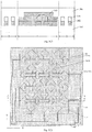
- Fig. 3 is a plane schematic diagram of a first conductive layer pattern of a touch structure provided by the embodiment;
- Fig. 5C2 is a plane schematic diagram of the touch structure.
- the touch structure is formed on a substrate.
- the method comprises following steps S101-S104.
- a first conductive layer 102 is first formed on a base substrate 101.
- a material of the base substrate 101 may comprise, for example, a polymer material, such as a polycycloolefin polymer material (COP), or the material of the base substrate 101 may comprise glass, quartz, ceramics, or the like, which is not limited in the embodiment.
- a material of the first conductive layer 102 may comprise, for example, a transparent conductive material, such as indium tin oxide (ITO), indium zinc oxide (IZO), or the like.
- the first conductive layer 102 may be formed on a surface of the base substrate 101 by, for example, a sputtering method or a deposition method.
- the first conductive layer 102 may be formed on the base substrate 101 by a magnetron sputtering method, a chemical vapor deposition method or the like.
- the base substrate 101 may also directly adopt a material that has been coated with the first conductive layer 102, for example, adopt a commercially available polycycloolefin polymer material (COP) having a surface coated with ITO.
- COP polycycloolefin polymer material
- the second conductive layer 103 is directly formed on the first conductive layer 102.
- the second conductive layer 103 may be, for example, a metal layer, and a material of the metal layer may comprise, for example, copper or copper alloy, aluminum or aluminum alloy, or the like.
- the second conductive layer 103 may be formed on a surface of the first conductive layer 102 by, for example, a sputtering method or the like.
- the second conductive layer 103 is patterned to form a second conductive layer pattern 1031.
- an etchant only having an etching effect on the second conductive layer 103 but having no etching effect on the first conductive layer 102 may be used.
- the second conductive layer 103 is the metal layer and the first conductive layer 102 is an indium tin oxide layer (ITO layer)
- an etchant such as hydrogen peroxide or the like, which has an etching effect on the metal layer but has no etching effect on the ITO, may be used to etch the second conductive layer 103, so as to form the second conductive layer pattern 1031. Because the etchant does not have the etching effect on the first conductive layer 102, the integrity of the first conductive layer 102 can be maintained.
- the touch structure may comprise a touch region 1 and a periphery region 2, and the second conductive layer pattern 1031 is formed in the periphery region 2.
- the second conductive layer 103 may be patterned by a photolithography process, and the photolithography process comprises steps of photoresist coating, exposing, developing, etching, and so on.
- the first conductive layer 102 is patterned to form a first conductive layer pattern.
- the first conductive layer 102 may be patterned by a photolithography process.
- the photolithography process comprises steps of photoresist coating, exposing, developing, etching, and so on.
- the first conductive layer 102 may be etched by aqua regia as an etchant to form the first conductive layer pattern.
- the second conductive layer pattern 1031 which has been formed may be covered by the photoresist pattern to be protected, so that the second conductive layer pattern 1031 is not adversely affected by the etchant during a process of etching the first conductive layer 102.
- the second conductive layer pattern 1031 or a portion may be used as an alignment mark to etch the first conductive layer 103, so as to form the first conductive layer pattern.
- the position of the second conductive layer pattern 1031 may be scanned by a photographing system of an exposure machine, and the alignment operation may be performed; alternatively, after the second conductive layer pattern 1031 is formed, an alignment mark is formed based on the second conductive layer pattern 1031, and the alignment mark is used for the alignment operation of the exposure machine, so that the formed first conductive layer pattern is aligned with the second conductive layer pattern 1031.
- the first conductive layer pattern may be formed, for example, in both the touch region 1 and the periphery region 2, and comprise a touch pattern in the touch region 1 and a periphery pattern 1022 in the periphery region 2.
- Fig. 3 is a plane schematic diagram of the first conductive layer pattern in the embodiment
- Fig. 2D is a sectional schematic diagram taken along line A-A of Fig. 3
- the touch pattern of the first conductive layer pattern in the touch region 1 comprises, for example, a first sensing line pattern 1021A formed along a first direction, such as an X direction in the figure, and the first sensing line pattern 1021A comprises a plurality of first sensing electrodes that are spaced apart from each other.
- the touch pattern further comprises a second sensing line pattern 1021B extending along a second direction, such as a Y direction in the figure, the second sensing line pattern 1021B passes through intervals of the plurality of first sensing electrodes 1021A.
- the first direction and the second direction are substantially perpendicular to each other.
- the touch region 1 in Fig. 2D only shows two first sensing electrodes comprised in the first sensing line pattern 1021A and one second sensing line pattern 1021B extending in the Y direction disposed at an interval between the two first sensing electrodes.
- the number of the first sensing electrodes comprised in the first sensing line pattern 1021A and the number of the second sensing line patterns 1021B may be more, and the embodiment is not limited in this aspect.
- the second conductive layer pattern 1031 and the periphery pattern 1022 of the first conductive layer pattern in the periphery region 2 may be, for example, lead wires of the first sensing line pattern 1021A and the second sensing line pattern 1021B, so as to connect the first sensing line pattern 1021A and the second sensing line pattern 1021B with a control unit 100 that performs functions such as calculating the touch position and so on.
- a position at which the periphery pattern 1022 of the first conductive layer pattern in the periphery region 2 is formed corresponds to a position at which the second conductive layer pattern 1031 is formed.
- the second conductive layer pattern 1031 is formed, when the periphery pattern 1022 of the first conductive layer pattern is etched, the second conductive layer pattern 1031 is coated with the photoresist, thereby preventing the etchant for etching the first conductive layer from corroding the second conductive layer pattern 1031.
- the method for manufacturing the touch structure provided by the embodiment is illustrated in Fig. 4 , and the method may further comprise steps S105-S107.
- Fig. 5A1 and Fig. 5A2 are respectively a sectional schematic diagram and a plane schematic diagram of the touch structure formed in this step (the sectional schematic diagram is obtained by taken along the line A-A as a hatching line in the plane schematic diagram.
- the touch region 1 in the sectional schematic diagram of Fig. 5A1 only shows two first sensing electrodes comprised in the first sensing line pattern 1021A and one second sensing line pattern 1021B extending in the Y direction disposed at the interval between the two first sensing electrodes).
- the touch region 1 in the sectional schematic diagram of Fig. 5A1 only shows two first sensing electrodes comprised in the first sensing line pattern 1021A and one second sensing line pattern 1021B extending in the Y direction disposed at the interval between the two first sensing electrodes).
- a first protective layer 104 may be formed on the first conductive layer pattern, and the first protective layer 104 is patterned to form a first protective layer pattern, and the first protective layer pattern exposes at least a portion of the plurality of first sensing electrodes.
- the portion of the plurality of first sensing electrodes may be exposed by a method of forming a via hole 1041 in the first protective layer pattern.
- the first protective layer pattern may cover or expose the second conductive layer pattern 1031.
- the first protective layer 104 may be, for example, an organic insulating layer, and a material of the organic insulating layer may comprise, for example, a polymer material such as resin or the like, and the organic insulating layer is formed on the first conductive layer pattern by a coating method or the like.
- the material and specific forming method of the first protective layer 104 are not limited by the embodiment.
- the first protective layer 104 may be patterned by a photolithography process to form the first protective layer pattern, and the photolithography process comprises steps of photoresist coating, exposing, developing, etching, and so on.
- a third conductive layer 105 may further be formed, and the third conductive layer 105 is patterned to form a third conductive layer pattern.
- the third conductive layer 105 may also be patterned by a photolithography process to form the third conductive layer pattern.
- the third conductive layer pattern may be formed, for example, on the first protective layer pattern which covers the first sensing line pattern 1021A, and formed on the portion exposed of the first sensing electrodes through the via hole 1041, so as to electrically connects the adjacent first sensing electrodes to each other.
- a second protective layer 106 may further be formed, and the second protective layer 106 is patterned to form a second protective layer pattern.
- the second protective layer 106 may also be patterned by a photolithography process to form the second protective layer pattern.
- the second protective layer pattern may cover, for example, the first conductive layer pattern and the third conductive layer pattern, for example, may further cover the second conductive layer pattern 1031, so as to protect each conductive layer and prevent the patterns from being oxidized.
- the second conductive layer is formed after the first conductive layer is formed, and the second conductive layer is first patterned, and then the first conductive layer is patterned, therefore, the more accurate alignment of the first conductive layer pattern and the second conductive layer pattern are achieved, and problems such as difficulty in aligning the second conductive layer pattern with the first conductive layer pattern due to a reason that the first conductive layer is relatively thin and the like are avoided.
- At least one embodiment of the present disclosure further provides another method of manufacturing a touch structure, the method also includes the steps S101-S104 in the above embodiment, in the embodiment, what is different from the above embodiment is the specific forming processes adopted in steps S101-S104.
- the method for manufacturing a touch structure provided by the embodiment is as follows.
- a first conductive layer 202 is formed on a base substrate 201.
- the forming method and the used material of the first conductive layer 202 are the same as those in the above embodiment.
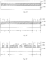
- the difference between this embodiment and the above embodiment is that in this embodiment, after the first conductive layer 202 is formed, a photoresist coating, exposing, and developing processes are performed on the first conductive layer 202 to form a first photoresist pattern 2020.
- the first photoresist pattern 2020 may be formed, for example, in the touch region 10. After the first photoresist pattern 2020 is formed, the first conductive layer 202 is not etched, and a subsequent forming process is performed.
- a second conductive layer 203 is formed on the first conductive layer 202 and the first photoresist pattern 2020.
- the forming method and the used material of the second conductive layer 203 are the same as those in the above embodiment, and are not described here again.
- the second conductive layer 203 is patterned to form a second conductive layer pattern.
- the method of patterning the second conductive layer 203 in this embodiment is different from that in the above embodiment.
- the photolithography process may be performed on the second conductive layer 203 to form the second conductive layer pattern by using the first photoresist pattern 2020 formed in the step S101 or a portion (for example, a specially manufactured pattern for alignment) as an alignment mark.
- the position of the first photoresist pattern 2020 may be scanned by a photographing system of an exposure machine, and the alignment operation may be performed; alternatively, because there is a protruding alignment mark (not shown in the figure) in the first conductive layer 202, in a case where the photoresist is coated, a thickness protruding portion corresponding to the alignment mark exists in the photoresist, so that the thickness protruding portion can be used for the alignment operation of the exposure machine, and then a subsequent process is performed. Finally, the alignment of the first conductive layer pattern with the second conductive layer pattern is achieved.
- the photolithography process is performed based on the above alignment operation, and steps of photoresist coating, exposing, and developing are performed on the second conductive layer 203 to form a second photoresist pattern 2030
- the second photoresist pattern 2030 may be formed, for example, in the periphery region 20.
- a same etchant is used to etch the second conductive layer 203 to form a second conductive layer pattern 2031 in the periphery region 20 and etch the first conductive layer 202 using the first photoresist pattern 2020 to form a first conductive layer pattern.
- the first conductive layer pattern comprises a first sensing line pattern 2021A and a second sensing line pattern 2021B that are in the touch region, and a periphery pattern 2022 in the periphery region 20.
- the etchant should have etching effects on both the material used for the first conductive layer 202 and the material used for the second conductive layer 203.
- the etchant may comprise, for example, a weak acid solution.
- an oxalic acid solution, a phosphoric acid solution or the like may be used for etching. Therefore, the two functional layers of the ITO transparent conductive layer and the metal layer are simultaneously etched by the same etchant.
- the second conductive layer 203 and the first conductive layer 202 are etched by the same etchant, after the second conductive layer pattern 2031 that is in an upper layer is formed, or where the etchant etches the second conductive layer 203 and contacts the first conductive layer 202, the first conductive layer 202 is further etched to form the first conductive layer pattern, and therefore the second conductive layer pattern 2031 and the first conductive layer pattern may be formed sequentially in a relatively fast time or almost simultaneously.
- the method of manufacturing the touch structure may also comprise the steps S105-S107 in the above embodiment, that is, the steps of forming the first protective layer pattern, the third conductive layer pattern, and the second protective layer pattern.
- the specific operation methods of these steps are the same as those in the above embodiment, and details are not described here again.
- substantially the same touch structure can be formed, and each conductive layer pattern of the touch structure is aligned more accurately, so that the touch sensing is sensitive and the function is stronger.
- At least one embodiment of the present disclosure further provides a touch structure, and the touch structure is manufactured by any one of the methods of manufacturing a touch structure provided by embodiments of the present disclosure.
- the touch structure may be, for example, a capacitive touch screen, for example, may be a surface type capacitive touch screen or a projected type capacitive touch screen, for example, may also be a self-capacitive touch screen or a mutual capacitive touch screen.
- the specific type of the touch structure is not limited in the embodiment. In the touch structure provided by the embodiment, the alignment of each conductive layer pattern is more accurate, so that the touch sensing is sensitive and the function is stronger.
- the embodiment provides a mutual capacitive touch screen
- the touch screen comprises a first sensing line pattern 3021A along the X direction and a second sensing line pattern 3021B along the Y direction that are formed on a base substrate (not shown).
- the first sensing line pattern 3021A comprises a plurality of first sensing electrodes that are spaced apart from each other, the second sensing line pattern 3021B is continuous and passes through intervals of the first sensing electrodes 3021A.
- the touch screen further comprises a first protective layer pattern 304 and a third conductive layer pattern 305, the first protective layer pattern 304 is formed at least on a portion, which corresponds to an interval of the first sensing electrodes 3021A, of the second sensing line pattern 3021B.
- the first protective layer pattern 304 is formed on surfaces of the first sensing line pattern 3021A and the second sensing line pattern 3021B and exposes a portion (not shown) of the first sensing electrodes 3021 A
- the third conductive layer pattern 305 is formed on the first protective layer pattern 304 and bridges the adjacent two first sensing electrodes having the interval through the exposed portion, and therefore the first sensing line pattern 3021A and the second sensing line pattern 3021B have intersecting portions and the first sensing line pattern 3021A and the second sensing line pattern 3021B are insulated by the first protective layer pattern 304 at the intersecting portions, so that capacitors are formed at the intersecting portions, and the first sensing line pattern 3021A and the second sensing line pattern 3021B respectively constitute two electrodes of the capacitors.
- the touch screen further comprises a metal line 3031 as a lead wire and a periphery pattern 3022 that is in the same layer as the first sensing line pattern 3021A and the second sensing line pattern 3021B, and the metal line 3031 and the periphery pattern 3022 connect the first sensing line pattern 3021A and the second sensing line pattern 3021B to a control unit 300 having functions such as calculating a touch point or the like. Therefore, in a case where a finger touches the touch screen, the finger affects the coupling between the two electrodes near the touch point, and therefore changes the capacitance between the two electrodes.
- the control unit 300 may receive the capacitance variation data, and calculate coordinates of each touch point according to the capacitance variation data.
- the control unit 300 can obtain the capacitance values of the intersections of all the first sensing line pattern 3021A and the second sensing line pattern 3021B, that is, the capacitance values of the two-dimensional plane of the whole touch screen, furthermore the control unit 300 can calculate the coordinates of each touch point on the touch screen, so that the touch operation is achieved.
- the mutual capacitive touch screen provided by the embodiment may further comprise structures such as other protective layers for protecting respective functional layers and so on, and details are not described in the embodiment.
- the electronic device comprises any one of the touch structures provided by the above embodiments of the present disclosure.
- the electronic device may be a display device.
- the display device comprises an array substrate and an opposite substrate (for example, a color filter substrate) that is assembled with the array substrate.
- the touch structure may be disposed on a protective cover plate, the protective cover plate is used to cover a display screen to protect the display screen, and a side, which is formed with the touch structure, of the protective cover plate faces the display screen. That is, a combination mode of the touch structure and the display screen is an OGS (One Glass Solution) mode.
- OGS One Glass Solution
- the touch structure may be disposed on a side of the opposite substrate that is far away from the array substrate, and a polarizer may be further disposed on a side of the touch structure that is far away from the opposite substrate. That is, a combination mode of the touch structure and the display screen is an On-Cell (external arrangement type) mode.
- the embodiment of the present disclosure does not limit the combination mode of the touch structure in the electronic device.
Landscapes
- Engineering & Computer Science (AREA)
- General Engineering & Computer Science (AREA)
- Theoretical Computer Science (AREA)
- Human Computer Interaction (AREA)
- Physics & Mathematics (AREA)
- General Physics & Mathematics (AREA)
- Manufacturing & Machinery (AREA)
- Microelectronics & Electronic Packaging (AREA)
- Computer Networks & Wireless Communication (AREA)
- Position Input By Displaying (AREA)
Applications Claiming Priority (2)
| Application Number | Priority Date | Filing Date | Title |
|---|---|---|---|
| CN201710725537.8A CN109426397B (zh) | 2017-08-22 | 2017-08-22 | 触控结构的制备方法、触控结构 |
| PCT/CN2018/082197 WO2019037433A1 (zh) | 2017-08-22 | 2018-04-08 | 触控结构的制备方法、触控结构 |
Publications (2)
| Publication Number | Publication Date |
|---|---|
| EP3674863A1 true EP3674863A1 (de) | 2020-07-01 |
| EP3674863A4 EP3674863A4 (de) | 2021-07-14 |
Family
ID=65439305
Family Applications (1)
| Application Number | Title | Priority Date | Filing Date |
|---|---|---|---|
| EP18788994.4A Withdrawn EP3674863A4 (de) | 2017-08-22 | 2018-04-08 | Verfahren zur herstellung einer berührungssteuerungsstruktur und berührungssteuerungsstruktur |
Country Status (5)
| Country | Link |
|---|---|
| US (1) | US11184985B2 (de) |
| EP (1) | EP3674863A4 (de) |
| JP (1) | JP7187319B2 (de) |
| CN (1) | CN109426397B (de) |
| WO (1) | WO2019037433A1 (de) |
Families Citing this family (2)
| Publication number | Priority date | Publication date | Assignee | Title |
|---|---|---|---|---|
| KR102783662B1 (ko) * | 2019-06-20 | 2025-03-20 | 삼성디스플레이 주식회사 | 표시 장치 |
| KR102835594B1 (ko) * | 2019-07-17 | 2025-07-21 | 삼성디스플레이 주식회사 | 입력감지장치 및 이를 포함하는 표시 장치 |
Family Cites Families (11)
| Publication number | Priority date | Publication date | Assignee | Title |
|---|---|---|---|---|
| CN101923412A (zh) * | 2009-06-16 | 2010-12-22 | 时纬科技股份有限公司 | 触摸屏及其制造方法 |
| JP5473990B2 (ja) | 2011-06-17 | 2014-04-16 | 日東電工株式会社 | 導電性積層体、パターン配線付き透明導電性積層体、および光学デバイス。 |
| TW201327510A (zh) * | 2011-12-16 | 2013-07-01 | Ind Tech Res Inst | 陣列基板的製造方法、顯示面板及其製造方法 |
| US9911550B2 (en) * | 2012-03-05 | 2018-03-06 | Apple Inc. | Touch sensitive device with multiple ablation fluence values |
| TWI476459B (zh) * | 2012-05-03 | 2015-03-11 | Innocom Tech Shenzhen Co Ltd | 彩色濾光片基板,及觸控顯示裝置 |
| CN103384451A (zh) * | 2012-05-04 | 2013-11-06 | 群康科技(深圳)有限公司 | 触控面板边缘走线的制作方法、触控面板及触控显示装置 |
| KR102122749B1 (ko) * | 2012-06-05 | 2020-06-15 | 쇼와 덴코 가부시키가이샤 | 기재막 및 소결 방법 |
| JP5813598B2 (ja) | 2012-08-27 | 2015-11-17 | 大日本印刷株式会社 | タッチパネルセンサ基板およびタッチパネルセンサ基板の製造方法 |
| CN105027041A (zh) | 2013-02-27 | 2015-11-04 | 凸版印刷株式会社 | 触摸面板和触摸面板的制造方法 |
| KR102204110B1 (ko) | 2014-02-05 | 2021-01-18 | 삼성디스플레이 주식회사 | 터치 스크린 패널 및 그 제조 방법 |
| CN105093636B (zh) * | 2015-09-21 | 2018-11-13 | 京东方科技集团股份有限公司 | 触控显示基板及其制备方法和触控显示面板 |
-
2017
- 2017-08-22 CN CN201710725537.8A patent/CN109426397B/zh active Active
-
2018
- 2018-04-08 WO PCT/CN2018/082197 patent/WO2019037433A1/zh not_active Ceased
- 2018-04-08 US US16/098,030 patent/US11184985B2/en active Active
- 2018-04-08 EP EP18788994.4A patent/EP3674863A4/de not_active Withdrawn
- 2018-04-08 JP JP2018557091A patent/JP7187319B2/ja active Active
Also Published As
| Publication number | Publication date |
|---|---|
| EP3674863A4 (de) | 2021-07-14 |
| JP7187319B2 (ja) | 2022-12-12 |
| US20210223915A1 (en) | 2021-07-22 |
| CN109426397B (zh) | 2020-08-04 |
| JP2020531930A (ja) | 2020-11-05 |
| US11184985B2 (en) | 2021-11-23 |
| CN109426397A (zh) | 2019-03-05 |
| WO2019037433A1 (zh) | 2019-02-28 |
Similar Documents
| Publication | Publication Date | Title |
|---|---|---|
| EP2386937B1 (de) | Kapazitiver Berührungsbildschirm und Verfahren zur Reduktion der Sichtbarkeit von Metallleitungen darin | |
| US8790865B2 (en) | Method of fabricating capacitive touch panel | |
| EP2737390B1 (de) | Kapazitiver berührungsbildschirm und herstellungsverfahren dafür | |
| US8847906B2 (en) | Touch device and method for manufacturing the same | |
| US9153385B2 (en) | Electrode structure of the touch panel, method thereof and touch panel | |
| US9671909B2 (en) | Mutual capacitance one glass solution touch panel and manufacture method thereof | |
| CN101751181B (zh) | 制作触控面板的方法 | |
| JP5942454B2 (ja) | タッチパネルセンサ、タッチパネル付表示装置およびタッチパネルセンサの製造方法 | |
| CN106020562B (zh) | 一种触控屏及其制作方法、外挂式触摸屏 | |
| CN103792711A (zh) | 一种触控显示面板及其制备方法 | |
| US8568599B1 (en) | Touch panel fabricating method | |
| CN103455203A (zh) | 触摸屏、其制作方法及显示装置 | |
| CN106681559B (zh) | 触控面板及其制造方法、触控显示装置 | |
| US9753572B2 (en) | Touch panel, method of fabricating the same and touch display device | |
| JP5471543B2 (ja) | タッチパネルセンサ製造方法およびタッチパネルセンサ | |
| US9430109B2 (en) | Touch screen panel and method for manufacturing the same, and display device | |
| US11184985B2 (en) | Method of manufacturing touch structure and touch structure | |
| EP3640776A1 (de) | Berührungsbildschirm und verfahren zur herstellung davon, berührungsanzeigevorrichtung | |
| WO2009005240A2 (en) | Pad for capacitance type touch panel and method of preparing touch panel using the same | |
| KR20190113931A (ko) | 전자 기판과 그 제조 방법, 및 전자 디바이스 | |
| KR20140078881A (ko) | 결정질 ito와 비정질 ito를 사용하는 터치패널 | |
| JP6676450B2 (ja) | タッチセンサ及びタッチセンサの製造方法 | |
| KR20150019571A (ko) | 터치 패널 및 제조 방법 | |
| CN203480465U (zh) | 触摸屏及显示装置 | |
| CN112783352B (zh) | 触摸屏的制备方法及触摸屏 |
Legal Events
| Date | Code | Title | Description |
|---|---|---|---|
| STAA | Information on the status of an ep patent application or granted ep patent |
Free format text: STATUS: UNKNOWN |
|
| STAA | Information on the status of an ep patent application or granted ep patent |
Free format text: STATUS: THE INTERNATIONAL PUBLICATION HAS BEEN MADE |
|
| PUAI | Public reference made under article 153(3) epc to a published international application that has entered the european phase |
Free format text: ORIGINAL CODE: 0009012 |
|
| STAA | Information on the status of an ep patent application or granted ep patent |
Free format text: STATUS: REQUEST FOR EXAMINATION WAS MADE |
|
| 17P | Request for examination filed |
Effective date: 20181030 |
|
| AK | Designated contracting states |
Kind code of ref document: A1 Designated state(s): AL AT BE BG CH CY CZ DE DK EE ES FI FR GB GR HR HU IE IS IT LI LT LU LV MC MK MT NL NO PL PT RO RS SE SI SK SM TR |
|
| AX | Request for extension of the european patent |
Extension state: BA ME |
|
| DAV | Request for validation of the european patent (deleted) | ||
| DAX | Request for extension of the european patent (deleted) | ||
| A4 | Supplementary search report drawn up and despatched |
Effective date: 20210616 |
|
| RIC1 | Information provided on ipc code assigned before grant |
Ipc: G06F 3/044 20060101AFI20210610BHEP Ipc: G06F 3/041 20060101ALI20210610BHEP |
|
| STAA | Information on the status of an ep patent application or granted ep patent |
Free format text: STATUS: THE APPLICATION HAS BEEN WITHDRAWN |
|
| 18W | Application withdrawn |
Effective date: 20220202 |