EP3675100A1 - Pixelschaltung und verfahren zum ansteuern derselben, anzeigevorrichtung - Google Patents
Pixelschaltung und verfahren zum ansteuern derselben, anzeigevorrichtung Download PDFInfo
- Publication number
- EP3675100A1 EP3675100A1 EP18830359.8A EP18830359A EP3675100A1 EP 3675100 A1 EP3675100 A1 EP 3675100A1 EP 18830359 A EP18830359 A EP 18830359A EP 3675100 A1 EP3675100 A1 EP 3675100A1
- Authority
- EP
- European Patent Office
- Prior art keywords
- transistor
- electrode
- sub
- circuit
- driving
- Prior art date
- Legal status (The legal status is an assumption and is not a legal conclusion. Google has not performed a legal analysis and makes no representation as to the accuracy of the status listed.)
- Granted
Links
Images






Classifications
-
- G—PHYSICS
- G09—EDUCATION; CRYPTOGRAPHY; DISPLAY; ADVERTISING; SEALS
- G09G—ARRANGEMENTS OR CIRCUITS FOR CONTROL OF INDICATING DEVICES USING STATIC MEANS TO PRESENT VARIABLE INFORMATION
- G09G3/00—Control arrangements or circuits, of interest only in connection with visual indicators other than cathode-ray tubes
- G09G3/20—Control arrangements or circuits, of interest only in connection with visual indicators other than cathode-ray tubes for presentation of an assembly of a number of characters, e.g. a page, by composing the assembly by combination of individual elements arranged in a matrix no fixed position being assigned to or needed to be assigned to the individual characters or partial characters
- G09G3/22—Control arrangements or circuits, of interest only in connection with visual indicators other than cathode-ray tubes for presentation of an assembly of a number of characters, e.g. a page, by composing the assembly by combination of individual elements arranged in a matrix no fixed position being assigned to or needed to be assigned to the individual characters or partial characters using controlled light sources
- G09G3/30—Control arrangements or circuits, of interest only in connection with visual indicators other than cathode-ray tubes for presentation of an assembly of a number of characters, e.g. a page, by composing the assembly by combination of individual elements arranged in a matrix no fixed position being assigned to or needed to be assigned to the individual characters or partial characters using controlled light sources using electroluminescent panels
- G09G3/32—Control arrangements or circuits, of interest only in connection with visual indicators other than cathode-ray tubes for presentation of an assembly of a number of characters, e.g. a page, by composing the assembly by combination of individual elements arranged in a matrix no fixed position being assigned to or needed to be assigned to the individual characters or partial characters using controlled light sources using electroluminescent panels semiconductive, e.g. using light-emitting diodes [LED]
- G09G3/3208—Control arrangements or circuits, of interest only in connection with visual indicators other than cathode-ray tubes for presentation of an assembly of a number of characters, e.g. a page, by composing the assembly by combination of individual elements arranged in a matrix no fixed position being assigned to or needed to be assigned to the individual characters or partial characters using controlled light sources using electroluminescent panels semiconductive, e.g. using light-emitting diodes [LED] organic, e.g. using organic light-emitting diodes [OLED]
-
- G—PHYSICS
- G09—EDUCATION; CRYPTOGRAPHY; DISPLAY; ADVERTISING; SEALS
- G09G—ARRANGEMENTS OR CIRCUITS FOR CONTROL OF INDICATING DEVICES USING STATIC MEANS TO PRESENT VARIABLE INFORMATION
- G09G3/00—Control arrangements or circuits, of interest only in connection with visual indicators other than cathode-ray tubes
- G09G3/20—Control arrangements or circuits, of interest only in connection with visual indicators other than cathode-ray tubes for presentation of an assembly of a number of characters, e.g. a page, by composing the assembly by combination of individual elements arranged in a matrix no fixed position being assigned to or needed to be assigned to the individual characters or partial characters
- G09G3/22—Control arrangements or circuits, of interest only in connection with visual indicators other than cathode-ray tubes for presentation of an assembly of a number of characters, e.g. a page, by composing the assembly by combination of individual elements arranged in a matrix no fixed position being assigned to or needed to be assigned to the individual characters or partial characters using controlled light sources
- G09G3/30—Control arrangements or circuits, of interest only in connection with visual indicators other than cathode-ray tubes for presentation of an assembly of a number of characters, e.g. a page, by composing the assembly by combination of individual elements arranged in a matrix no fixed position being assigned to or needed to be assigned to the individual characters or partial characters using controlled light sources using electroluminescent panels
- G09G3/32—Control arrangements or circuits, of interest only in connection with visual indicators other than cathode-ray tubes for presentation of an assembly of a number of characters, e.g. a page, by composing the assembly by combination of individual elements arranged in a matrix no fixed position being assigned to or needed to be assigned to the individual characters or partial characters using controlled light sources using electroluminescent panels semiconductive, e.g. using light-emitting diodes [LED]
- G09G3/3208—Control arrangements or circuits, of interest only in connection with visual indicators other than cathode-ray tubes for presentation of an assembly of a number of characters, e.g. a page, by composing the assembly by combination of individual elements arranged in a matrix no fixed position being assigned to or needed to be assigned to the individual characters or partial characters using controlled light sources using electroluminescent panels semiconductive, e.g. using light-emitting diodes [LED] organic, e.g. using organic light-emitting diodes [OLED]
- G09G3/3225—Control arrangements or circuits, of interest only in connection with visual indicators other than cathode-ray tubes for presentation of an assembly of a number of characters, e.g. a page, by composing the assembly by combination of individual elements arranged in a matrix no fixed position being assigned to or needed to be assigned to the individual characters or partial characters using controlled light sources using electroluminescent panels semiconductive, e.g. using light-emitting diodes [LED] organic, e.g. using organic light-emitting diodes [OLED] using an active matrix
- G09G3/3233—Control arrangements or circuits, of interest only in connection with visual indicators other than cathode-ray tubes for presentation of an assembly of a number of characters, e.g. a page, by composing the assembly by combination of individual elements arranged in a matrix no fixed position being assigned to or needed to be assigned to the individual characters or partial characters using controlled light sources using electroluminescent panels semiconductive, e.g. using light-emitting diodes [LED] organic, e.g. using organic light-emitting diodes [OLED] using an active matrix with pixel circuitry controlling the current through the light-emitting element
-
- G—PHYSICS
- G09—EDUCATION; CRYPTOGRAPHY; DISPLAY; ADVERTISING; SEALS
- G09G—ARRANGEMENTS OR CIRCUITS FOR CONTROL OF INDICATING DEVICES USING STATIC MEANS TO PRESENT VARIABLE INFORMATION
- G09G3/00—Control arrangements or circuits, of interest only in connection with visual indicators other than cathode-ray tubes
- G09G3/20—Control arrangements or circuits, of interest only in connection with visual indicators other than cathode-ray tubes for presentation of an assembly of a number of characters, e.g. a page, by composing the assembly by combination of individual elements arranged in a matrix no fixed position being assigned to or needed to be assigned to the individual characters or partial characters
- G09G3/22—Control arrangements or circuits, of interest only in connection with visual indicators other than cathode-ray tubes for presentation of an assembly of a number of characters, e.g. a page, by composing the assembly by combination of individual elements arranged in a matrix no fixed position being assigned to or needed to be assigned to the individual characters or partial characters using controlled light sources
- G09G3/30—Control arrangements or circuits, of interest only in connection with visual indicators other than cathode-ray tubes for presentation of an assembly of a number of characters, e.g. a page, by composing the assembly by combination of individual elements arranged in a matrix no fixed position being assigned to or needed to be assigned to the individual characters or partial characters using controlled light sources using electroluminescent panels
- G09G3/32—Control arrangements or circuits, of interest only in connection with visual indicators other than cathode-ray tubes for presentation of an assembly of a number of characters, e.g. a page, by composing the assembly by combination of individual elements arranged in a matrix no fixed position being assigned to or needed to be assigned to the individual characters or partial characters using controlled light sources using electroluminescent panels semiconductive, e.g. using light-emitting diodes [LED]
- G09G3/3208—Control arrangements or circuits, of interest only in connection with visual indicators other than cathode-ray tubes for presentation of an assembly of a number of characters, e.g. a page, by composing the assembly by combination of individual elements arranged in a matrix no fixed position being assigned to or needed to be assigned to the individual characters or partial characters using controlled light sources using electroluminescent panels semiconductive, e.g. using light-emitting diodes [LED] organic, e.g. using organic light-emitting diodes [OLED]
- G09G3/3266—Details of drivers for scan electrodes
-
- G—PHYSICS
- G09—EDUCATION; CRYPTOGRAPHY; DISPLAY; ADVERTISING; SEALS
- G09G—ARRANGEMENTS OR CIRCUITS FOR CONTROL OF INDICATING DEVICES USING STATIC MEANS TO PRESENT VARIABLE INFORMATION
- G09G2300/00—Aspects of the constitution of display devices
- G09G2300/04—Structural and physical details of display devices
- G09G2300/0421—Structural details of the set of electrodes
- G09G2300/0426—Layout of electrodes and connections
-
- G—PHYSICS
- G09—EDUCATION; CRYPTOGRAPHY; DISPLAY; ADVERTISING; SEALS
- G09G—ARRANGEMENTS OR CIRCUITS FOR CONTROL OF INDICATING DEVICES USING STATIC MEANS TO PRESENT VARIABLE INFORMATION
- G09G2300/00—Aspects of the constitution of display devices
- G09G2300/04—Structural and physical details of display devices
- G09G2300/0439—Pixel structures
- G09G2300/0465—Improved aperture ratio, e.g. by size reduction of the pixel circuit, e.g. for improving the pixel density or the maximum displayable luminance or brightness
-
- G—PHYSICS
- G09—EDUCATION; CRYPTOGRAPHY; DISPLAY; ADVERTISING; SEALS
- G09G—ARRANGEMENTS OR CIRCUITS FOR CONTROL OF INDICATING DEVICES USING STATIC MEANS TO PRESENT VARIABLE INFORMATION
- G09G2300/00—Aspects of the constitution of display devices
- G09G2300/08—Active matrix structure, i.e. with use of active elements, inclusive of non-linear two terminal elements, in the pixels together with light emitting or modulating elements
- G09G2300/0809—Several active elements per pixel in active matrix panels
- G09G2300/0819—Several active elements per pixel in active matrix panels used for counteracting undesired variations, e.g. feedback or autozeroing
-
- G—PHYSICS
- G09—EDUCATION; CRYPTOGRAPHY; DISPLAY; ADVERTISING; SEALS
- G09G—ARRANGEMENTS OR CIRCUITS FOR CONTROL OF INDICATING DEVICES USING STATIC MEANS TO PRESENT VARIABLE INFORMATION
- G09G2300/00—Aspects of the constitution of display devices
- G09G2300/08—Active matrix structure, i.e. with use of active elements, inclusive of non-linear two terminal elements, in the pixels together with light emitting or modulating elements
- G09G2300/0809—Several active elements per pixel in active matrix panels
- G09G2300/0842—Several active elements per pixel in active matrix panels forming a memory circuit, e.g. a dynamic memory with one capacitor
-
- G—PHYSICS
- G09—EDUCATION; CRYPTOGRAPHY; DISPLAY; ADVERTISING; SEALS
- G09G—ARRANGEMENTS OR CIRCUITS FOR CONTROL OF INDICATING DEVICES USING STATIC MEANS TO PRESENT VARIABLE INFORMATION
- G09G2300/00—Aspects of the constitution of display devices
- G09G2300/08—Active matrix structure, i.e. with use of active elements, inclusive of non-linear two terminal elements, in the pixels together with light emitting or modulating elements
- G09G2300/0809—Several active elements per pixel in active matrix panels
- G09G2300/0842—Several active elements per pixel in active matrix panels forming a memory circuit, e.g. a dynamic memory with one capacitor
- G09G2300/0861—Several active elements per pixel in active matrix panels forming a memory circuit, e.g. a dynamic memory with one capacitor with additional control of the display period without amending the charge stored in a pixel memory, e.g. by means of additional select electrodes
-
- G—PHYSICS
- G09—EDUCATION; CRYPTOGRAPHY; DISPLAY; ADVERTISING; SEALS
- G09G—ARRANGEMENTS OR CIRCUITS FOR CONTROL OF INDICATING DEVICES USING STATIC MEANS TO PRESENT VARIABLE INFORMATION
- G09G2310/00—Command of the display device
- G09G2310/02—Addressing, scanning or driving the display screen or processing steps related thereto
- G09G2310/0202—Addressing of scan or signal lines
- G09G2310/0216—Interleaved control phases for different scan lines in the same sub-field, e.g. initialization, addressing and sustaining in plasma displays that are not simultaneous for all scan lines
-
- G—PHYSICS
- G09—EDUCATION; CRYPTOGRAPHY; DISPLAY; ADVERTISING; SEALS
- G09G—ARRANGEMENTS OR CIRCUITS FOR CONTROL OF INDICATING DEVICES USING STATIC MEANS TO PRESENT VARIABLE INFORMATION
- G09G2310/00—Command of the display device
- G09G2310/02—Addressing, scanning or driving the display screen or processing steps related thereto
- G09G2310/0243—Details of the generation of driving signals
- G09G2310/0245—Clearing or presetting the whole screen independently of waveforms, e.g. on power-on
-
- G—PHYSICS
- G09—EDUCATION; CRYPTOGRAPHY; DISPLAY; ADVERTISING; SEALS
- G09G—ARRANGEMENTS OR CIRCUITS FOR CONTROL OF INDICATING DEVICES USING STATIC MEANS TO PRESENT VARIABLE INFORMATION
- G09G2320/00—Control of display operating conditions
- G09G2320/02—Improving the quality of display appearance
- G09G2320/0257—Reduction of after-image effects
-
- G—PHYSICS
- G09—EDUCATION; CRYPTOGRAPHY; DISPLAY; ADVERTISING; SEALS
- G09G—ARRANGEMENTS OR CIRCUITS FOR CONTROL OF INDICATING DEVICES USING STATIC MEANS TO PRESENT VARIABLE INFORMATION
- G09G2320/00—Control of display operating conditions
- G09G2320/04—Maintaining the quality of display appearance
- G09G2320/043—Preventing or counteracting the effects of ageing
- G09G2320/045—Compensation of drifts in the characteristics of light emitting or modulating elements
Definitions
- the present disclosure relates to the field of display technology, and in particular, to a pixel circuit, a method of driving the same, and a display device.
- OLED Organic Light Emitting Diode
- LCD liquid crystal displays
- a pixel circuit including: a light emitting device; a driving sub-circuit configured to drive the light emitting device, the driving sub-circuit including a driving transistor configured to generate a driving current flowing through the light emitting device so that the light emitting device emits light; and a reset sub-circuit configured to reset a voltage between a gate electrode and a second electrode of the driving transistor.
- the reset sub-circuit is connected to an initial voltage terminal and the driving sub-circuit, and the reset sub-circuit is configured to write an initial voltage of the initial voltage terminal to the gate electrode and the second electrode of the driving transistor of the driving sub-circuit.
- a first electrode of the driving transistor is configured to be in a float state during a process in which the reset sub-circuit resets the voltage between the gate electrode and the second electrode of the driving transistor.
- the pixel circuit further includes: a write sub-circuit configured to write a data voltage from a data voltage terminal to the driving sub-circuit under the control of a first scan signal terminal.
- the pixel circuit further includes: a compensation sub-circuit configured to compensate a threshold voltage of the driving transistor.
- the pixel circuit further includes: a light emission control sub-circuit configured to transmit the driving current to the light emitting device.
- the reset sub-circuit is configured to write the initial voltage of the initial voltage terminal to the light emitting device.
- a part of the reset sub-circuit is reused as at least a part of the compensation sub-circuit.
- the reset sub-circuit includes a first transistor and a second transistor; a gate electrode of the first transistor is connected to a second scan signal terminal, a first electrode of the first transistor is connected to the gate electrode of the driving transistor, and a second electrode of the first transistor is connected to an initial voltage terminal; a gate electrode of the second transistor is connected to a light emission control signal terminal, a first electrode of the second transistor is connected to a second electrode of the driving transistor, and a second electrode of the second transistor is connected to the gate electrode of the driving transistor.
- the reset sub-circuit further includes a third transistor; a gate electrode of the third transistor is connected to a second scan signal terminal, a first electrode of the third transistor is connected to the light emitting device, and a second electrode of the third transistor is connected to the initial voltage terminal.
- a part of the reset sub-circuit is reused as at least a part of the light emission control sub-circuit.
- the reset sub-circuit includes a first transistor, a second transistor and a third transistor, a gate electrode of the first transistor is connected to a second scan signal terminal, a first electrode of the first transistor is connected to the gate electrode of the driving transistor, and a second electrode of the first transistor is connected to the initial voltage terminal; a gate electrode of the second transistor is connected to the second scan signal terminal, a first electrode of the second transistor is connected to the light emitting device, and a second electrode of the second transistor is connected to the initial voltage terminal; and a gate electrode of the third transistor is connected to the first scan signal terminal, a first electrode of the third transistor is connected to the second electrode of the driving transistor, and a second electrode of the third transistor is connected to the light emitting device.
- the compensation sub-circuit includes the second transistor.
- the light emission control sub-circuit includes a fourth transistor and a fifth transistor; a gate electrode of the fourth transistor is connected to the light emission control signal terminal, a first electrode of the fourth transistor is connected to the first voltage terminal, and a second electrode of the fourth transistor is connected to the first electrode of the driving transistor; and a gate electrode of the fifth transistor is connected to the light emission control signal terminal, a first electrode of the fifth transistor is connected to the second electrode of the driving transistor, and a second electrode of the fifth transistor is connected to the light emitting device.
- the light emission control sub-circuit includes the third transistor and the fourth transistor; the gate electrode of the fourth transistor is connected to the light emission control signal terminal, the first electrode of the fourth transistor is connected to the first voltage terminal, and the second electrode of the fourth transistor is connected to the first electrode of the driving transistor.
- the compensation sub-circuit includes a fifth transistor; a gate electrode of the fifth transistor is connected to the first scan signal terminal, a first electrode of the fifth transistor is connected to the second electrode of the driving transistor, and a second electrode of the fifth transistor is connected to the gate electrode of the driving transistor.
- the write sub-circuit includes a sixth transistor, a first electrode of the sixth transistor is connected to the first scan signal terminal, a first electrode of the sixth transistor is connected to the data voltage terminal, and a second electrode of the sixth transistor is connected to the first electrode of the driving transistor.
- the driving sub-circuit further includes a storage capacitor; one end of the storage capacitor is connected to the first voltage terminal and the other end of the storage capacitor is connected to the gate electrode of the driving transistor.
- a display device including the above pixel circuit of the present disclosure.
- the display device includes a display panel on which sub-pixels arranged in a matrix are disposed, the pixel circuits being arranged in the sub-pixels; except the first row of sub-pixels, the second scan signal terminals of the pixel circuits in the next row of sub-pixels are connected to the first scan signal terminals of the pixel circuits in the previous row of sub-pixels.
- a method for driving the pixel circuit comprising: setting the first electrode of the driving transistor to a float state, and writing, by the reset sub-circuit, an initial voltage of the initial voltage terminal to the gate electrode and the second electrode of the driving transistor in the driving sub-circuit; writing, by the writing sub-circuit, a data voltage of the data voltage terminal to the driving sub-circuit according to a control signal provided by the first scan signal terminal; generating, by the diving sub-circuit, a driving current according to the first voltage terminal, the second voltage terminal, and the data voltage written to the driving sub-circuit; and emitting light by the light emitting device according to the driving current.
- the method further includes: compensating, by the compensation sub-circuit, a threshold voltage of the driving transistor in the driving sub-circuit.
- the reset sub-circuit is connected to the second scan signal terminal and the light emission control signal terminal;
- the reset sub-circuit includes a first transistor and a second transistor, wherein a gate electrode of the first transistor is connected to the second scan signal terminal, a first electrode of the first transistor is connected to the gate electrode of the driving transistor, and a second electrode of the first transistor is connected to the initial voltage terminal;
- a gate electrode of the second transistor is connected to the light emission control signal terminal, a first electrode of the second transistor is connected to a second electrode of the driving transistor, a second electrode of the second transistor is connected to the gate electrode of the driving transistor, and the driving transistor is a P-type transistor
- the step of setting the first electrode of the driving transistor to a float state and writing, by the reset sub-circuit, an initial voltage of the initial voltage terminal to the gate electrode and the second electrode of the driving transistor in the driving sub-circuit includes: setting the first electrode of the driving transistor to a float state; providing a signal of the second scan signal terminal
- the reset sub-circuit is connected to the first scan signal terminal, the second scan signal terminal, and the anode of the light emitting device;
- the reset sub-circuit comprises a first transistor, a second transistor and a third transistor, wherein a gate electrode of the first transistor is connected to the second scan signal terminal, a first electrode of the first transistor is connected to the gate electrode of the driving transistor, and a second electrode of the first transistor is connected to the initial voltage terminal;
- a gate electrode of the second transistor is connected to the second scan signal terminal, a first electrode of the second transistor is connected to the anode of the light emitting device, and a second electrode of the second transistor is connected to the initial voltage terminal;
- a gate electrode of the third transistor is connected to the first scan signal terminal, a first electrode of the third transistor is connected to a second electrode of the driving transistor, a second electrode of the third transistor is connected to the anode of the light emitting device, wherein the driving transistor is a P-type transistor, the step of setting the first electrode
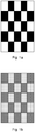
- an OLED display switches between pictures of different gray-scales, for example, from a picture of black-and-white blocks shown in FIG. 1a to a pure gray-scale picture having a gray-scale value of 128, a short-term afterimage will occur and an image shown in FIG. 1b will be displayed, on which an afterimage of the previous frame of black-and-white blocks occurs.
- the above-mentioned short-term afterimage disappears after one minute, and the display shows a pure gray-scale picture having a gray-scale value of 128 as shown in FIG. 1c .
- the above-mentioned short-term afterimage has an impact on the display effect.
- Embodiments of the present disclosure provide a pixel circuit, a method of driving the same, and a display device.
- a reset sub-circuit in the pixel circuit can set a DTFT to an OFF-Bias state at the end of a reset stage.
- a gate-source voltage Vgs of DTFTs in different sub-pixels is at the bottom of the characteristic curve, with the same corresponding current Ids, which is very small.
- the brightness of each sub-pixel needs to be increased, i.e., the current Ids of the DTFT in each sub-pixel needs to be increased, so that hole trapping is needed at the interface between the semiconductor layer and the gate insulating layer of the DTFT in each sub-pixel.
- the hole trapping paths are the same for the DTFTs, thereby solving the above-mentioned problem of short-term afterimage.
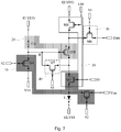
- a pixel circuit including a reset sub-circuit 10, a driving sub-circuit 20, a write sub-circuit 30, a compensation sub-circuit 40, a light emission control sub-circuit 50, and a light emitting device L.
- the above described driving sub-circuit 20 includes a drive transistor (hereinafter referred to as DTFT), a first electrode of which is connected to the write sub-circuit 30.
- DTFT drive transistor
- the driving sub-circuit 20 is further connected to a first voltage terminal ELVDD.
- the driving sub-circuit 20 further includes a storage capacitor Cst.
- One end of the storage capacitor Cst is connected to the first voltage terminal ELVDD and the other end of the storage capacitor Cst is connected to a gate electrode of DTFT. In this way, the storage capacitor Cst can ensure the stability of a gate voltage Vg of DTFT.
- the reset sub-circuit 10 is connected to an initial voltage terminal Vint and the driving sub-circuit 20.
- the reset sub-circuit 10 is configured to write an initial voltage of the initial voltage terminal Vint to a gate electrode and a second of the DTFT of the driving sub-circuit 20, a first electrode of the DTFT being in a float state during a reset stage.
- the type of DTFT is not limited in this application and can be either an N-type transistor or a P-type transistor.
- the first electrode of the DTFT is one of a source electrode and a drain electrode
- the second electrode of the DTFT is the other of the source electrode and the drain electrode.
- the DTFT is a P-type enhancement transistor.
- the first electrode of the DTFT is a source electrode and the second electrode is a drain electrode.
- Vgs Vint - Vth
- the DTFT is in an OFF-Bias state.
- the turn-off condition is Vgs ⁇ Vth and Vth is a negative value.
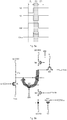
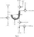
- FIG. 1d The process of the magnetic hysteresis effect is shown in FIG. 1d , wherein the dot dash line in FIG. 1 is a characteristic curve of DTFT current Ids and Vgs when the source-drain voltage of the DTFT in a sub-pixel displaying a white picture of the OLED display is Vds1.
- the dotted line is a characteristic curve of DTFT current Ids and Vgs when the source-drain voltage of the DTFT in a sub-pixel displaying a black picture is Vds3.
- the solid line is a characteristic curve of DTFT current and Vgs when the source-drain voltage of the DTFT in a sub-pixel displaying a gray scale picture of a gray-scale value of 128 is Vds2.
- the brightness of the sub-pixel displaying the white picture needs to be reduced, and the current Ids of the DTFT in the sub-pixel needs to be reduced, so that hole detrapping, from A1 to A2, is needed at the interface between the semiconductor layer and the gate insulating layer of the DTFT in the sub-pixel.
- the Vgs value changes from V_ w to V_ g.
- the brightness of the sub-pixel displaying the black picture needs to be increased, and the current Ids of the DTFT in the sub-pixel needs to be increased, so that hole trapping, from A3 to A4, is needed at the interface between the semiconductor layer and the gate insulating layer of the DTFT in the sub-pixel.
- the Vgs value changes from V_b to V_g.
- points a2 and a4 which are reached to voltage V-g along different paths corresponds to different currents Ids values, so that there is a brightness difference between a sub-pixel switching from the white picture to the gray-scale picture and a sub-pixel switching from the black picture to the gray-scale picture, resulting in a short-term afterimage phenomenon as shown in FIG. 1c .
- both of the above points A2 and A4 reach point B, and the afterimage disappears.
- the hole trapping paths are the same for the various DTFTs, thereby solving the above-mentioned problem of short-term afterimage.
- the pixel circuit provided by the present disclosure can solve the problem of short-term afterimage, and taking the display refresh rate required to display pictures by the display panel into account, there is no need to maintain the displayed image still.
- the reset sub-circuit 10 is further connected to the anode of the light emitting device L.
- the reset sub-circuit 10 is configured to write an initial voltage of the initial voltage terminal Vint to the anode of the light emitting device L. In this way, it is possible to prevent a voltage of the previous image frame remaining on the anode of the light emitting device L from affecting the image displayed in the next image frame.
- the voltage remaining on the anode of the light emitting device L will cause the driving current I OLED flowing through the light emitting device L to increase when the image of the next image frame is displayed, resulting in the brightness of the sub-pixel being larger than expected, which will reduce the contrast of the displayed image.
- the cathode of the light emitting device L is connected to a second voltage terminal ELVSS.
- the light emitting device L may be a light emitting diode (LED) or an organic light emitting diode (OLED), which is not limited in the present disclosure.
- the write sub-circuit 30 is connected to a first scan signal terminal S1, a data voltage terminal Data, and the driving sub-circuit 20.
- the write sub-circuit 30 is configured to write a data voltage (Vdata) of the data voltage terminal Data to the driving sub-circuit 20 under the control of the first scan signal terminal S1. Therefore, the magnitude of the driving current I OLED generated by the driving sub-circuit 20 for driving the light emitting device L to emit light can be matched with the above data voltage.
- the compensation sub-circuit 40 is connected to the driving sub-circuit 20. This compensation sub-circuit 40 is configured to compensate a threshold voltage Vth of the DTFT in the driving sub-circuit 20.
- the light emission control sub-circuit 50 is connected to the light emission control signal terminal EM, the first voltage terminal ELVDD, the driving sub-circuit 20, and the anode of the light emitting device L.
- the light emission control sub-circuit 50 is configured to, under the control of the light emission control signal terminal EM, transmit a driving current I OLED generated by the driving sub-circuit 20 under the action of the first voltage terminal ELVDD, the second voltage terminal ELVSS and the data voltage (Vdata) written to the driving sub-circuit 20 to the light emitting device L.
- the light emitting device L is configured to emit light according to the driving current IOLED.
- the first voltage terminal ELVDD is configured to output a constant high level.
- the second voltage terminal ELVSS is configured to output a constant low level, for example, the second voltage terminal ELVSS may be connected to a ground terminal.
- terms "high” and “low” used herein only indicate the relative magnitude relationship between the input voltages.
- a part of the reset sub-circuit 10 is reused as at least a part of the compensation sub-circuit 40 described above.
- the reset sub-circuit 10 in the case where the reset sub-circuit 10 is still connected to the second scan signal terminal S2, the light emission control signal terminal EM, and the anode of the light emitting device L, the reset sub-circuit 10 includes a first transistor M1 and a second transistor M2.
- a gate electrode of the first transistor M1 is connected to the second scan signal terminal S2, a first electrode of the first transistor M1 is connected to the gate electrode of the DTFT, and a second electrode of the first transistor M1 is connected to the initial voltage terminal Vint;
- a gate electrode of the second transistor M2 is connected to the light emission control signal terminal EM, a first electrode of the second transistor M2 is connected to a second electrode of the DTFT, and a second electrode of the second transistor M2 is connected to the gate electrode of the DTFT.
- the reset sub-circuit 10 in the case where the reset sub-circuit 10 is connected to the anode of the light emitting device L, the reset sub-circuit 10 further includes a third transistor M3.
- a gate electrode of the third transistor M3 is connected to the second scan signal terminal S2, a first electrode of the third transistor M3 is connected to the anode of the light emitting device L, and a second electrode of the third transistor M3 is connected to the initial voltage terminal Vint.
- the compensation sub-circuit 40 is connected to the light emission control signal terminal EM, and the compensation sub-circuit 40 includes the second transistor M2 described above. Therefore, the reset sub-circuit 10 and the compensation sub-circuit 40 share the second transistor M2.
- the light emission control sub-circuit 50 includes a fourth transistor M4 and a fifth transistor M5.
- a gate electrode of the fourth transistor M4 is connected to the light emission control signal terminal EM, a first electrode of the fourth transistor M4 is connected to the first voltage terminal ELVDD, and a second electrode of the fourth transistor M4 is connected to the first electrode of the DTFT.
- a gate electrode of the fifth transistor M5 is connected to the light emission control signal terminal EM, a first electrode of the fifth transistor M5 is connected to the second electrode of the DTFT, and a second electrode of the fifth transistor M5 is connected to the anode of the light emitting device L.
- the write sub-circuit 30 includes a sixth transistor M6, a gate electrode of the sixth transistor M6 is connected to the first scan signal terminal S1, a first electrode of the sixth transistor M6 is connected to the data voltage terminal Data, and a second electrode of the sixth transistor M6 is connected to the first electrode of the DTFT.
- the second transistor M2 is an N-type transistor and the other transistors are P-type transistors.
- the second transistor M2 may be a P-type transistor and the other transistors are N-type transistors.
- the first electrode is a source electrode and the second electrode is a drain electrode;
- the first electrode is a drain electrode and the second electrode is a source electrode.
- each of the transistors described above may be an enhancement transistor or a depletion transistor.
- the second transistor M2 is an N-type transistor
- the other transistors are P-type transistors
- each of the transistor is an enhancement transistor, as an example.
- the image frame described above includes a reset stage P1, a write compensation stage P2, and a light emission stage P3.
- DTFT is turned on by the initial voltage terminal Vint, and the gate-source voltage of the DTFT Vgs ⁇ Vth at this time.
- the source electrode (i.e., the first electrode) of the DTFT is in a float state during the reset stage P1.
- the cutoff condition is Vgs ⁇ Vth and Vth is negative.
- the third transistor M3 is turned on, so that the initial voltage of the initial voltage terminal Vint is output to the anode of the light emitting device L through the third transistor M3, and the anode of the light emitting transistor L is reset to improve the contrast of the displayed image.
- the fourth transistor M4, the fifth transistor M5, and the sixth transistor M6 are turned off.
- the sixth transistor M6 is turned on, thereby writing the data voltage Vdata output from the data voltage terminal Data to the source electrode of the DTFT through the sixth transistor M6.
- the source electrode of the DTFT is no longer in the float state, node B can be kept at a low level by the storage capacitor Cst, and at that point DTFT is turned on.
- the second transistor M2 under the control of the light emission control signal terminal EM, the second transistor M2 remains in the ON state.
- the data voltage Vdata at the data voltage terminal Data charges the storage capacitor Cst through the sixth transistor M6, the DTFT and the second transistor M2, the storage capacitor Cst in turn charges the gate electrode (i.e., point B) of the DTFT, until the voltage at point B reaches Vdata + Vth.
- V B Vdata + Vth
- the DTFT is in the OFF-Bias state.
- the cutoff condition is Vgs ⁇ Vth and Vth is negative. In this way, the threshold voltage Vth of the DTFT is locked to the gate electrode of the DTFT, thereby realizing compensation of the threshold voltage Vth of the DTFT.
- the first transistor M1, the third transistor M3, the fourth transistor M4, and the fifth transistor M5 are in the OFF state.
- the light emission control signal terminal EM outputs a low level, and the fourth transistor M4 and the fifth transistor M5 are turned on.
- the first transistor M1, the second transistor M2, the third transistor M3, and the sixth transistor M6 are in the OFF state.
- k is a current constant associated with the DTFT and is related to process parameters and geometric dimensions of the DTFT, such as electron mobility ⁇ , capacitance per unit area C ox , aspect ratio W/L, etc.
- the threshold voltage Vth drifts for DTFTs of different pixel units, resulting in different threshold voltages Vth of the various DTFTs. From the above formula (1), it can be seen that the driving current I OLED for driving the light emitting device L to emit light is independent of the threshold voltage Vth of the DTFT, thereby eliminating the influence of the threshold voltage Vth of the DTFT on the light emitting brightness of the light emitting device L, and improving the uniformity of the brightness of the light emitting device L.
- the second transistor M2 is an N-type transistor and the other transistors are P-type transistors. If the second transistor M2 is a P-type transistor and the other transistors are N-type transistors, the control process is similar, but some control signals need to be inverted.
- the above reset sub-circuit 10 is arranged in such a way that, for example, a part of the reset sub-circuit 10 is reused as at least a part of the light emission control sub-circuit 50.
- the reset sub-circuit 10 in the case where the reset sub-circuit 10 is connected to the anode of the light emitting device L, the reset sub-circuit 10 is further connected to the first scan signal terminal S1 and the second scan signal terminal S2.
- the reset sub-circuit 10 includes a first transistor M1, a second transistor M2, and a third transistor M3.
- a gate electrode of the first transistor M1 is connected to the second scan signal terminal S2
- a first electrode of the first transistor M1 is connected to the gate electrode of the DTFT
- a second electrode of the first transistor M1 is connected to the initial voltage terminal Vint.
- a gate electrode of the second transistor M2 is connected to the second scan signal terminal S2, a first electrode of the second transistor M2 is connected to the anode of the light emitting device L, and a second electrode of the second transistor M2 is connected to the initial voltage terminal Vint.
- a gate electrode of the third transistor M3 is connected to the first scan signal terminal S1, a first electrode of the third transistor M3 is connected to the second electrode of the DTFT, and a second electrode of the third transistor M3 is connected to the anode of the light emitting device L.
- the light emission control sub-circuit 50 is further connected to the first scan signal terminal S1.
- the light emission control sub-circuit 50 includes the third transistor M3 described above. Therefore, the reset sub-circuit 10 and the light emission control sub-circuit 50 share the third transistor M3.
- the light emission control sub-circuit 50 further includes a fourth transistor M4.
- a gate electrode of the fourth transistor M4 is connected to the light emission control signal terminal EM, a first electrode of the fourth transistor M4 is connected to the first voltage terminal ELVDD, and a second electrode of the fourth transistor M4 is connected to the first electrode of the DTFT.
- the compensation sub-circuit 40 is connected to the first scan signal terminal S1.
- the compensation sub-circuit 40 includes a fifth transistor M5.
- a gate electrode of the fifth transistor M5 is connected to the first scan signal terminal S1
- a first electrode of the fifth transistor M5 is connected to the second electrode of the DTFT
- a second electrode of the fifth transistor M5 is connected to the gate electrode of the DTFT.
- the write sub-circuit 30 includes a sixth transistor M6, a gate electrode of the sixth transistor M6 is connected to the first scan signal terminal S1, a first electrode of the sixth transistor M6 is connected to the data voltage terminal Data, and a second electrode of the sixth transistor M6 is connected to the first electrode of the DTFT.
- the third transistor M3 is an N-type transistor and the other transistors are P-type transistors.
- the third transistor M3 may be a P-type transistor and the other transistors are N-type transistors.
- each of the above transistors may be an enhancement transistor or a depletion transistor.
- the third transistor M3 is an N-type transistor
- the other transistors are P-type transistors
- each of the transistors is an enhancement transistor, as an example.
- the first transistor M1 and the second transistor M2 are turned on.
- An initial voltage of the initial voltage terminal Vint is transmitted to the gate electrode of the DTFT through the first transistor M1 and to the anode of the light emitting device L through the second transistor M2, to reset the gate electrode of the DTFT and the anode of the light emitting device L, respectively.
- the third transistor M3 is turned on, the initial voltage of the initial voltage terminal Vint is transmitted to the drain electrode (i.e., the second electrode) of the DTFT through the second transistor M2 and the third transistor M3, and the source electrode (i.e., the first electrode) of DTFT is in a float state in the reset stage P1.
- the fourth transistor M4, the fifth transistor M5, and the sixth transistor M6 are turned off.
- the data voltage Vdata at the data voltage terminal Data charges the gate electrode (i.e., point B) of the DTFT through the sixth transistor M6, the DTFT and the fifth transistor M5, until the voltage at point B reaches Vdata + Vth.
- the threshold voltage Vth of the DTFT is locked to the gate electrode of the DTFT, thereby realizing compensation of the threshold voltage Vth of the DTFT.
- the first transistor M1, the second transistor M2, the third transistor M3, and the fourth transistor M4 are in the OFF state.
- the light emission control signal terminal EM outputs a low level, and the third transistor M3 and the fourth transistor M4 are turned on.
- the first transistor M1, the second transistor M2, the fifth transistor M5, and the sixth transistor M6 are in the OFF state.
- the driving current I OLED for driving the light emitting device L to emit light is independent of the threshold voltage Vth of the DTFT, thereby eliminating the influence of the threshold voltage Vth of the DTFT on the light emitting brightness of the light emitting device L, and improving the uniformity of the brightness of the light emitting device L.
- the third transistor M3 is an N-type transistor and the other transistors are P-type transistors. If the third transistor M3 is a P-type transistor and the other transistors are N-type transistors, the control process is similar, but some control signals need to be inverted.
- An embodiment of the present disclosure provides a display device including any one of the pixel circuits described above.
- the pixel circuit in the display device has the same structure and beneficial effect as the pixel circuits provided in the previous embodiments, and will not be described herein.
- the display device may be a display device including an LED display or an OLED display with current-driven light emitting devices.
- the display device can be a television, a mobile phone, a tablet computer, etc.
- the display device includes a display panel with sub-pixels arranged in a matrix as shown in FIG. 11 , and the pixel circuits are arranged in the sub-pixels.
- the second scan signal terminals S2 of the pixel circuits in the next row of (nth row) sub-pixel Pixel are connected to the first scan signal terminals S1 of the pixel circuits in the previous row ((n-1)th row) of sub-pixels, where n ⁇ 1 and n is a positive integer.
- the signal terminals of adjacent two rows of sub-pixels are partially shared, so that the purpose of reducing the number of signal terminals can be achieved, resulting in a simpler wiring structure.
- An embodiment of the present disclosure provides a method for driving any one of the pixel circuits described above, in an image frame, the method including the following steps.
- the reset sub-circuit 10 writes the initial voltage of the initial voltage terminal Vint to the gate electrode and the second electrode of the DTFT in the driving sub-circuit 20 as shown in FIG. 2 , the first electrode of the DTFT being in a float state in the reset stage P1.
- a low level is input to the second scan signal terminal S2, and a high level is input to the first scan signal terminal S1 and the light emission control signal terminal EM.
- the control method includes the following steps.
- the first transistor M1 is turned on.
- the voltage of the initial voltage terminal Vint is written to the gate electrode of the DTFT through the first transistor M1.
- the second transistor M2 under the control of the light emission control signal terminal EM, the second transistor M2 is turned on, the gate electrode of the DTFT is electrically connected to the drain electrode (i.e., the second electrode) of the DTFT, and the source electrode (i.e., the first electrode) of the DTFT is in a float state in the reset stage P1.
- the control method includes the following steps.
- the first transistor M1 and the second transistor M2 are turned on.
- the third transistor M3 is turned on.
- the initial voltage of the initial voltage terminal Vint is written to the gate electrode of the DTFT through the first transistor M1.
- the initial voltage of the initial voltage terminal Vint is written to the anode of the light emitting device L through the second transistor M2.
- the initial voltage of the initial voltage terminal Vint is written to the drain electrode (i.e., the second electrode) of the DTFT through the second transistor M2 and the third transistor M3, and the source electrode (i.e., the first electrode) of the DTFT is in a float state during the reset stage P1.
- the specific reset process has been described above and will not be repeated herein.
- the write sub-circuit 30 writes the data voltage Vdata of the data voltage terminal Data to the driving sub-circuit 20 under the control of the first scan signal terminal S1.
- the compensation sub-circuit 40 compensates the threshold voltage Vth of DTFT in the driving sub-circuit 20.
- a high level is input to the second scan signal terminal S2 and the light emission control signal terminal EM, and a low level is input to the first scan signal terminal S1; a data signal Vdata is input to the data signal terminal Data.
- the specific compensation process has been described above and will not be repeated herein.
- a driving current I OLED is generated by the drive sub-circuit 20 under the action of the first voltage terminal ELVDD, the second voltage terminal ELVSS, and the data voltage Vdata written to the driving sub-circuit 20.
- the light emission control sub-circuit 50 transmits the driving current I OLED to the light emitting device L under the control of the light emission control signal terminal EM.
- the light emitting device L emits light according to the driving current IOLED.
- a high level is input to the second scan signal terminal 2 and the first scan signal terminal S1 and a low level is input to the light-emitting control signal terminal EM.
- the specific light emitting process has been described above, and will not be repeated herein.
Landscapes
- Engineering & Computer Science (AREA)
- Physics & Mathematics (AREA)
- Computer Hardware Design (AREA)
- General Physics & Mathematics (AREA)
- Theoretical Computer Science (AREA)
- Control Of Indicators Other Than Cathode Ray Tubes (AREA)
- Control Of El Displays (AREA)
Applications Claiming Priority (2)
| Application Number | Priority Date | Filing Date | Title |
|---|---|---|---|
| CN201710749623.2A CN107452331B (zh) | 2017-08-25 | 2017-08-25 | 一种像素电路及其驱动方法、显示装置 |
| PCT/CN2018/088703 WO2019037499A1 (zh) | 2017-08-25 | 2018-05-28 | 像素电路及其驱动方法、显示装置 |
Publications (3)
| Publication Number | Publication Date |
|---|---|
| EP3675100A1 true EP3675100A1 (de) | 2020-07-01 |
| EP3675100A4 EP3675100A4 (de) | 2021-08-04 |
| EP3675100B1 EP3675100B1 (de) | 2024-07-24 |
Family
ID=60494102
Family Applications (1)
| Application Number | Title | Priority Date | Filing Date |
|---|---|---|---|
| EP18830359.8A Active EP3675100B1 (de) | 2017-08-25 | 2018-05-28 | Pixelschaltung und verfahren zum ansteuern derselben, anzeigevorrichtung |
Country Status (4)
| Country | Link |
|---|---|
| US (3) | US11244611B2 (de) |
| EP (1) | EP3675100B1 (de) |
| CN (1) | CN107452331B (de) |
| WO (1) | WO2019037499A1 (de) |
Cited By (2)
| Publication number | Priority date | Publication date | Assignee | Title |
|---|---|---|---|---|
| EP3739567A4 (de) * | 2018-01-10 | 2021-10-06 | Boe Technology Group Co., Ltd. | Pixelschaltung, ansteuerungsverfahren dafür und anzeigetafel |
| US11289010B2 (en) | 2019-05-22 | 2022-03-29 | Boe Technology Group Co., Ltd. | Pixel circuit with photo-sensing function, a driving method, and a display apparatus |
Families Citing this family (39)
| Publication number | Priority date | Publication date | Assignee | Title |
|---|---|---|---|---|
| CN107452331B (zh) * | 2017-08-25 | 2023-12-05 | 京东方科技集团股份有限公司 | 一种像素电路及其驱动方法、显示装置 |
| CN110164375B (zh) | 2018-03-16 | 2021-01-22 | 京东方科技集团股份有限公司 | 像素补偿电路、驱动方法、电致发光显示面板及显示装置 |
| CN108538241A (zh) | 2018-06-29 | 2018-09-14 | 京东方科技集团股份有限公司 | 像素电路及其驱动方法、显示装置 |
| CN109102778A (zh) | 2018-11-15 | 2018-12-28 | 京东方科技集团股份有限公司 | 像素驱动电路及其驱动方法、显示装置 |
| CN109448637A (zh) | 2019-01-04 | 2019-03-08 | 京东方科技集团股份有限公司 | 一种像素驱动电路及其驱动方法、显示面板 |
| CN109584795A (zh) | 2019-01-29 | 2019-04-05 | 京东方科技集团股份有限公司 | 像素驱动电路、像素驱动方法和显示装置 |
| CN109817165B (zh) * | 2019-03-08 | 2021-04-20 | 京东方科技集团股份有限公司 | 像素驱动电路、像素驱动方法、显示面板和显示装置 |
| CN110033734B (zh) * | 2019-04-25 | 2021-08-10 | 京东方科技集团股份有限公司 | 一种显示驱动电路及其驱动方法、显示装置 |
| CN112424856B (zh) * | 2019-06-03 | 2023-03-14 | 京东方科技集团股份有限公司 | 像素电路、像素电路的驱动方法、显示装置及其驱动方法 |
| CN110197644A (zh) * | 2019-06-10 | 2019-09-03 | 武汉华星光电半导体显示技术有限公司 | 像素驱动电路 |
| CN113366562A (zh) * | 2019-07-12 | 2021-09-07 | 深圳市柔宇科技股份有限公司 | 像素单元、阵列基板与显示终端 |
| CN113168806B (zh) * | 2019-09-03 | 2023-07-21 | 京东方科技集团股份有限公司 | 像素驱动电路、像素驱动方法、显示面板及显示装置 |
| CN113096602A (zh) * | 2019-12-23 | 2021-07-09 | 深圳市柔宇科技股份有限公司 | 像素单元、显示面板与电子装置 |
| CN111243526A (zh) * | 2020-01-19 | 2020-06-05 | 京东方科技集团股份有限公司 | 像素电路、显示装置及驱动方法 |
| KR102743888B1 (ko) * | 2020-02-04 | 2024-12-19 | 삼성디스플레이 주식회사 | 화소 및 표시장치 |
| CN111179854A (zh) * | 2020-02-19 | 2020-05-19 | 京东方科技集团股份有限公司 | 像素驱动电路及其驱动方法、显示装置 |
| US12073787B2 (en) * | 2020-05-29 | 2024-08-27 | Chengdu Boe Optoelectronics Technology Co., Ltd. | Display panel |
| CN111508426B (zh) * | 2020-05-29 | 2022-04-15 | 京东方科技集团股份有限公司 | 像素电路及其驱动方法、显示面板 |
| CN111739471B (zh) * | 2020-08-06 | 2022-02-22 | 武汉天马微电子有限公司 | 一种显示面板、驱动方法及显示装置 |
| CN115104148B8 (zh) * | 2020-11-30 | 2026-02-06 | 京东方科技集团股份有限公司 | 像素电路、驱动方法、显示基板和显示装置 |
| CN114694572B (zh) * | 2020-12-28 | 2024-04-23 | 华为技术有限公司 | 驱动电路、显示装置及电子设备 |
| CN112908245B (zh) * | 2021-02-24 | 2022-09-23 | 昆山国显光电有限公司 | 像素电路及其驱动方法、显示面板 |
| CN113066434B (zh) | 2021-03-24 | 2023-07-18 | 京东方科技集团股份有限公司 | 像素驱动电路及其驱动方法、显示面板 |
| WO2022266875A1 (zh) * | 2021-06-23 | 2022-12-29 | 京东方科技集团股份有限公司 | 像素电路、驱动方法和显示装置 |
| US12217673B2 (en) | 2021-06-23 | 2025-02-04 | Chengdu Boe Optoelectronics Technology Co., Ltd. | Pixel circuit, driving method and display device |
| CN113471264B (zh) * | 2021-06-30 | 2022-10-04 | 武汉天马微电子有限公司 | 一种显示面板和显示装置 |
| CN113808532B (zh) | 2021-08-25 | 2022-09-27 | 武汉华星光电半导体显示技术有限公司 | 像素电路及显示面板 |
| CN113870758B (zh) * | 2021-09-18 | 2022-10-21 | 云谷(固安)科技有限公司 | 像素电路及其驱动方法、显示面板 |
| CN113870789A (zh) * | 2021-10-27 | 2021-12-31 | 成都京东方光电科技有限公司 | 一种像素驱动电路、其驱动方法及显示装置 |
| CN114187871B (zh) * | 2021-12-10 | 2023-03-21 | 北京欧铼德微电子技术有限公司 | 电压调整方法及装置、电子设备 |
| CN118475973A (zh) | 2021-12-29 | 2024-08-09 | 夏普株式会社 | 显示装置 |
| CN114446238A (zh) * | 2022-01-26 | 2022-05-06 | 合肥维信诺科技有限公司 | 像素驱动电路、驱动方法及显示装置 |
| CN115188333B (zh) * | 2022-07-15 | 2026-01-13 | 京东方科技集团股份有限公司 | 一种像素电路、其驱动方法及显示装置 |
| CN115662355A (zh) * | 2022-10-25 | 2023-01-31 | 北京京东方技术开发有限公司 | 像素电路、驱动方法、显示面板及显示装置 |
| KR20240100748A (ko) * | 2022-12-23 | 2024-07-02 | 엘지디스플레이 주식회사 | 스테이지 트랜지스터를 포함하는 표시장치 |
| CN116364029A (zh) * | 2023-03-27 | 2023-06-30 | 厦门天马微电子有限公司 | 一种显示面板及显示装置 |
| KR20250021192A (ko) * | 2023-08-03 | 2025-02-12 | 삼성디스플레이 주식회사 | 표시 장치 |
| CN117524103A (zh) * | 2023-12-06 | 2024-02-06 | 武汉华星光电半导体显示技术有限公司 | 像素驱动电路及显示面板 |
| CN121281431A (zh) * | 2025-12-10 | 2026-01-06 | 武汉天马微电子有限公司 | 显示面板以及显示装置 |
Family Cites Families (29)
| Publication number | Priority date | Publication date | Assignee | Title |
|---|---|---|---|---|
| KR100514183B1 (ko) | 2003-09-08 | 2005-09-13 | 삼성에스디아이 주식회사 | 유기 전계발광 표시장치의 픽셀구동회로 및 그 구동방법 |
| KR100673759B1 (ko) * | 2004-08-30 | 2007-01-24 | 삼성에스디아이 주식회사 | 발광 표시장치 |
| KR100741973B1 (ko) * | 2005-08-12 | 2007-07-23 | 삼성에스디아이 주식회사 | 유기 전계발광 표시장치 |
| KR101499236B1 (ko) * | 2008-12-29 | 2015-03-06 | 삼성디스플레이 주식회사 | 표시 장치 및 그 구동 방법 |
| KR101152580B1 (ko) * | 2010-06-30 | 2012-06-01 | 삼성모바일디스플레이주식회사 | 화소 및 이를 이용한 유기전계발광 표시장치 |
| KR101152466B1 (ko) * | 2010-06-30 | 2012-06-01 | 삼성모바일디스플레이주식회사 | 화소 및 이를 이용한 유기전계발광 표시장치 |
| KR102113650B1 (ko) * | 2013-12-27 | 2020-06-03 | 삼성디스플레이 주식회사 | 표시 장치 및 그 구동 방법 |
| KR102257941B1 (ko) | 2014-06-17 | 2021-05-31 | 삼성디스플레이 주식회사 | 유기 발광 표시 장치 |
| CN104200771B (zh) * | 2014-09-12 | 2017-03-01 | 上海天马有机发光显示技术有限公司 | 像素电路、阵列基板及显示装置 |
| CN104269133B (zh) | 2014-09-25 | 2016-07-06 | 合肥鑫晟光电科技有限公司 | 一种像素电路及有机电致发光显示面板 |
| CN104318902B (zh) * | 2014-11-19 | 2017-05-31 | 上海天马有机发光显示技术有限公司 | 有机发光显示器的像素电路及驱动方法、有机发光显示器 |
| KR102363339B1 (ko) * | 2014-11-26 | 2022-02-15 | 삼성디스플레이 주식회사 | 유기 발광 표시 장치 및 이의 구동 방법 |
| CN104616621B (zh) * | 2015-02-05 | 2017-04-12 | 京东方科技集团股份有限公司 | 一种像素电路及其驱动方法、显示装置 |
| CN106297645A (zh) * | 2015-05-15 | 2017-01-04 | 上海和辉光电有限公司 | 像素驱动电路和显示装置 |
| KR102464283B1 (ko) * | 2015-06-29 | 2022-11-09 | 삼성디스플레이 주식회사 | 화소 및 이를 이용한 유기전계발광 표시장치와 그의 구동방법 |
| KR102383741B1 (ko) * | 2015-09-10 | 2022-04-08 | 삼성디스플레이 주식회사 | 화소, 화소를 포함하는 유기전계발광 표시장치 및 화소의 구동 방법 |
| KR102509185B1 (ko) * | 2015-09-25 | 2023-03-13 | 엘지디스플레이 주식회사 | 유기발광다이오드 표시 패널, 이를 구비하는 유기발광다이오드 표시 장치 및 이의 구동 방법 |
| JP2018013567A (ja) * | 2016-07-20 | 2018-01-25 | 株式会社ジャパンディスプレイ | 表示装置 |
| CN106448557B (zh) * | 2016-12-26 | 2019-05-03 | 深圳市华星光电技术有限公司 | 发光驱动电路及有机发光显示器 |
| CN106531076B (zh) | 2017-01-12 | 2019-03-01 | 京东方科技集团股份有限公司 | 一种像素电路、显示面板及其驱动方法 |
| CN106652915A (zh) * | 2017-02-09 | 2017-05-10 | 鄂尔多斯市源盛光电有限责任公司 | 一种像素电路、显示面板、显示装置及驱动方法 |
| CN106981268B (zh) * | 2017-05-17 | 2019-05-10 | 京东方科技集团股份有限公司 | 一种像素电路及其驱动方法、显示装置 |
| KR102369624B1 (ko) * | 2017-06-30 | 2022-03-03 | 엘지디스플레이 주식회사 | 표시패널과 이를 이용한 전계 발광 표시장치 |
| CN107452331B (zh) * | 2017-08-25 | 2023-12-05 | 京东方科技集团股份有限公司 | 一种像素电路及其驱动方法、显示装置 |
| CN107358918B (zh) | 2017-08-25 | 2023-11-21 | 京东方科技集团股份有限公司 | 一种像素电路及其驱动方法、显示装置 |
| CN207134126U (zh) * | 2017-08-25 | 2018-03-23 | 京东方科技集团股份有限公司 | 一种像素电路及显示装置 |
| CN107358920B (zh) * | 2017-09-08 | 2019-09-24 | 京东方科技集团股份有限公司 | 像素驱动电路及其驱动方法及显示装置 |
| CN107680537B (zh) * | 2017-11-21 | 2019-11-29 | 上海天马微电子有限公司 | 一种像素电路的驱动方法 |
| CN108665852A (zh) * | 2018-07-23 | 2018-10-16 | 京东方科技集团股份有限公司 | 像素电路、驱动方法、有机发光显示面板及显示装置 |
-
2017
- 2017-08-25 CN CN201710749623.2A patent/CN107452331B/zh active Active
-
2018
- 2018-05-28 WO PCT/CN2018/088703 patent/WO2019037499A1/zh not_active Ceased
- 2018-05-28 EP EP18830359.8A patent/EP3675100B1/de active Active
- 2018-05-28 US US16/318,321 patent/US11244611B2/en active Active
-
2022
- 2022-01-12 US US17/573,987 patent/US20220139321A1/en not_active Abandoned
-
2023
- 2023-01-04 US US18/150,092 patent/US11984081B2/en active Active
Cited By (2)
| Publication number | Priority date | Publication date | Assignee | Title |
|---|---|---|---|---|
| EP3739567A4 (de) * | 2018-01-10 | 2021-10-06 | Boe Technology Group Co., Ltd. | Pixelschaltung, ansteuerungsverfahren dafür und anzeigetafel |
| US11289010B2 (en) | 2019-05-22 | 2022-03-29 | Boe Technology Group Co., Ltd. | Pixel circuit with photo-sensing function, a driving method, and a display apparatus |
Also Published As
| Publication number | Publication date |
|---|---|
| US11984081B2 (en) | 2024-05-14 |
| WO2019037499A1 (zh) | 2019-02-28 |
| EP3675100A4 (de) | 2021-08-04 |
| CN107452331B (zh) | 2023-12-05 |
| CN107452331A (zh) | 2017-12-08 |
| US11244611B2 (en) | 2022-02-08 |
| US20200388214A1 (en) | 2020-12-10 |
| US20220139321A1 (en) | 2022-05-05 |
| EP3675100B1 (de) | 2024-07-24 |
| US20230145828A1 (en) | 2023-05-11 |
Similar Documents
| Publication | Publication Date | Title |
|---|---|---|
| US11984081B2 (en) | Pixel circuit and method of driving the same, display device | |
| US11699394B2 (en) | Pixel circuit, driving method thereof and display device | |
| US12300172B2 (en) | Pixel circuit and driving method therefor and display panel | |
| US12322335B2 (en) | Pixel circuit and driving method therefor, and display panel | |
| US10923032B2 (en) | Pixel circuit and method of driving the same, display panel, and display apparatus | |
| US11798473B2 (en) | Pixel driving circuit and display panel | |
| US10991303B2 (en) | Pixel circuit and driving method thereof, display device | |
| US20210327347A1 (en) | Pixel circuit and driving method thereof, and display panel | |
| US9666132B2 (en) | Pixel circuit, method for driving the same and display apparatus | |
| CN104871233B (zh) | 显示设备、用于驱动显示设备的方法以及电子装置 | |
| EP3723077A1 (de) | Pixelschaltung und ansteuerungsverfahren dafür sowie anzeigevorrichtung | |
| US20200082757A1 (en) | Pixel driving circuit and method for driving the same, pixel unit and display panel | |
| US20170116919A1 (en) | Pixel circuit and driving method thereof, display device | |
| CN107564478A (zh) | 一种显示面板及其显示方法、显示装置 | |
| US20190066580A1 (en) | Pixel circuit, driving method thereof, and display device | |
| US10140922B2 (en) | Pixel driving circuit and driving method thereof and display device | |
| GB2620507A (en) | Pixel circuit and driving method therefor and display panel | |
| US11514844B2 (en) | Pixel drive circuit, pixel unit, driving method, array substrate, and display apparatus | |
| CN207134126U (zh) | 一种像素电路及显示装置 | |
| JP2025526530A (ja) | 画素回路およびその駆動方法、表示パネル、表示装置 | |
| US11908408B2 (en) | Display device and driving method therefor | |
| JP2010026209A (ja) | 表示装置 |
Legal Events
| Date | Code | Title | Description |
|---|---|---|---|
| STAA | Information on the status of an ep patent application or granted ep patent |
Free format text: STATUS: UNKNOWN |
|
| STAA | Information on the status of an ep patent application or granted ep patent |
Free format text: STATUS: THE INTERNATIONAL PUBLICATION HAS BEEN MADE |
|
| PUAI | Public reference made under article 153(3) epc to a published international application that has entered the european phase |
Free format text: ORIGINAL CODE: 0009012 |
|
| STAA | Information on the status of an ep patent application or granted ep patent |
Free format text: STATUS: REQUEST FOR EXAMINATION WAS MADE |
|
| 17P | Request for examination filed |
Effective date: 20190117 |
|
| AK | Designated contracting states |
Kind code of ref document: A1 Designated state(s): AL AT BE BG CH CY CZ DE DK EE ES FI FR GB GR HR HU IE IS IT LI LT LU LV MC MK MT NL NO PL PT RO RS SE SI SK SM TR |
|
| AX | Request for extension of the european patent |
Extension state: BA ME |
|
| DAV | Request for validation of the european patent (deleted) | ||
| DAX | Request for extension of the european patent (deleted) | ||
| A4 | Supplementary search report drawn up and despatched |
Effective date: 20210702 |
|
| RIC1 | Information provided on ipc code assigned before grant |
Ipc: G09G 3/32 20160101AFI20210628BHEP Ipc: G09G 3/3233 20160101ALI20210628BHEP Ipc: G09G 3/3258 20160101ALI20210628BHEP |
|
| STAA | Information on the status of an ep patent application or granted ep patent |
Free format text: STATUS: EXAMINATION IS IN PROGRESS |
|
| 17Q | First examination report despatched |
Effective date: 20230515 |
|
| GRAP | Despatch of communication of intention to grant a patent |
Free format text: ORIGINAL CODE: EPIDOSNIGR1 |
|
| STAA | Information on the status of an ep patent application or granted ep patent |
Free format text: STATUS: GRANT OF PATENT IS INTENDED |
|
| INTG | Intention to grant announced |
Effective date: 20240404 |
|
| GRAS | Grant fee paid |
Free format text: ORIGINAL CODE: EPIDOSNIGR3 |
|
| GRAA | (expected) grant |
Free format text: ORIGINAL CODE: 0009210 |
|
| STAA | Information on the status of an ep patent application or granted ep patent |
Free format text: STATUS: THE PATENT HAS BEEN GRANTED |
|
| AK | Designated contracting states |
Kind code of ref document: B1 Designated state(s): AL AT BE BG CH CY CZ DE DK EE ES FI FR GB GR HR HU IE IS IT LI LT LU LV MC MK MT NL NO PL PT RO RS SE SI SK SM TR |
|
| REG | Reference to a national code |
Ref country code: GB Ref legal event code: FG4D |
|
| REG | Reference to a national code |
Ref country code: CH Ref legal event code: EP |
|
| REG | Reference to a national code |
Ref country code: DE Ref legal event code: R096 Ref document number: 602018072262 Country of ref document: DE |
|
| REG | Reference to a national code |
Ref country code: IE Ref legal event code: FG4D |
|
| REG | Reference to a national code |
Ref country code: LT Ref legal event code: MG9D |
|
| REG | Reference to a national code |
Ref country code: NL Ref legal event code: MP Effective date: 20240724 |
|
| PG25 | Lapsed in a contracting state [announced via postgrant information from national office to epo] |
Ref country code: PT Free format text: LAPSE BECAUSE OF FAILURE TO SUBMIT A TRANSLATION OF THE DESCRIPTION OR TO PAY THE FEE WITHIN THE PRESCRIBED TIME-LIMIT Effective date: 20241125 |
|
| REG | Reference to a national code |
Ref country code: AT Ref legal event code: MK05 Ref document number: 1707074 Country of ref document: AT Kind code of ref document: T Effective date: 20240724 |
|
| PG25 | Lapsed in a contracting state [announced via postgrant information from national office to epo] |
Ref country code: NL Free format text: LAPSE BECAUSE OF FAILURE TO SUBMIT A TRANSLATION OF THE DESCRIPTION OR TO PAY THE FEE WITHIN THE PRESCRIBED TIME-LIMIT Effective date: 20240724 |
|
| PG25 | Lapsed in a contracting state [announced via postgrant information from national office to epo] |
Ref country code: PT Free format text: LAPSE BECAUSE OF FAILURE TO SUBMIT A TRANSLATION OF THE DESCRIPTION OR TO PAY THE FEE WITHIN THE PRESCRIBED TIME-LIMIT Effective date: 20241125 Ref country code: NL Free format text: LAPSE BECAUSE OF FAILURE TO SUBMIT A TRANSLATION OF THE DESCRIPTION OR TO PAY THE FEE WITHIN THE PRESCRIBED TIME-LIMIT Effective date: 20240724 |
|
| PG25 | Lapsed in a contracting state [announced via postgrant information from national office to epo] |
Ref country code: NO Free format text: LAPSE BECAUSE OF FAILURE TO SUBMIT A TRANSLATION OF THE DESCRIPTION OR TO PAY THE FEE WITHIN THE PRESCRIBED TIME-LIMIT Effective date: 20241024 |
|
| PG25 | Lapsed in a contracting state [announced via postgrant information from national office to epo] |
Ref country code: GR Free format text: LAPSE BECAUSE OF FAILURE TO SUBMIT A TRANSLATION OF THE DESCRIPTION OR TO PAY THE FEE WITHIN THE PRESCRIBED TIME-LIMIT Effective date: 20241025 Ref country code: FI Free format text: LAPSE BECAUSE OF FAILURE TO SUBMIT A TRANSLATION OF THE DESCRIPTION OR TO PAY THE FEE WITHIN THE PRESCRIBED TIME-LIMIT Effective date: 20240724 Ref country code: PL Free format text: LAPSE BECAUSE OF FAILURE TO SUBMIT A TRANSLATION OF THE DESCRIPTION OR TO PAY THE FEE WITHIN THE PRESCRIBED TIME-LIMIT Effective date: 20240724 |
|
| PG25 | Lapsed in a contracting state [announced via postgrant information from national office to epo] |
Ref country code: BG Free format text: LAPSE BECAUSE OF FAILURE TO SUBMIT A TRANSLATION OF THE DESCRIPTION OR TO PAY THE FEE WITHIN THE PRESCRIBED TIME-LIMIT Effective date: 20240724 |
|
| PG25 | Lapsed in a contracting state [announced via postgrant information from national office to epo] |
Ref country code: LV Free format text: LAPSE BECAUSE OF FAILURE TO SUBMIT A TRANSLATION OF THE DESCRIPTION OR TO PAY THE FEE WITHIN THE PRESCRIBED TIME-LIMIT Effective date: 20240724 |
|
| PG25 | Lapsed in a contracting state [announced via postgrant information from national office to epo] |
Ref country code: IS Free format text: LAPSE BECAUSE OF FAILURE TO SUBMIT A TRANSLATION OF THE DESCRIPTION OR TO PAY THE FEE WITHIN THE PRESCRIBED TIME-LIMIT Effective date: 20241124 Ref country code: AT Free format text: LAPSE BECAUSE OF FAILURE TO SUBMIT A TRANSLATION OF THE DESCRIPTION OR TO PAY THE FEE WITHIN THE PRESCRIBED TIME-LIMIT Effective date: 20240724 |
|
| PG25 | Lapsed in a contracting state [announced via postgrant information from national office to epo] |
Ref country code: HR Free format text: LAPSE BECAUSE OF FAILURE TO SUBMIT A TRANSLATION OF THE DESCRIPTION OR TO PAY THE FEE WITHIN THE PRESCRIBED TIME-LIMIT Effective date: 20240724 |
|
| PG25 | Lapsed in a contracting state [announced via postgrant information from national office to epo] |
Ref country code: ES Free format text: LAPSE BECAUSE OF FAILURE TO SUBMIT A TRANSLATION OF THE DESCRIPTION OR TO PAY THE FEE WITHIN THE PRESCRIBED TIME-LIMIT Effective date: 20240724 Ref country code: RS Free format text: LAPSE BECAUSE OF FAILURE TO SUBMIT A TRANSLATION OF THE DESCRIPTION OR TO PAY THE FEE WITHIN THE PRESCRIBED TIME-LIMIT Effective date: 20241024 |
|
| PG25 | Lapsed in a contracting state [announced via postgrant information from national office to epo] |
Ref country code: RS Free format text: LAPSE BECAUSE OF FAILURE TO SUBMIT A TRANSLATION OF THE DESCRIPTION OR TO PAY THE FEE WITHIN THE PRESCRIBED TIME-LIMIT Effective date: 20241024 Ref country code: PL Free format text: LAPSE BECAUSE OF FAILURE TO SUBMIT A TRANSLATION OF THE DESCRIPTION OR TO PAY THE FEE WITHIN THE PRESCRIBED TIME-LIMIT Effective date: 20240724 Ref country code: NO Free format text: LAPSE BECAUSE OF FAILURE TO SUBMIT A TRANSLATION OF THE DESCRIPTION OR TO PAY THE FEE WITHIN THE PRESCRIBED TIME-LIMIT Effective date: 20241024 Ref country code: LV Free format text: LAPSE BECAUSE OF FAILURE TO SUBMIT A TRANSLATION OF THE DESCRIPTION OR TO PAY THE FEE WITHIN THE PRESCRIBED TIME-LIMIT Effective date: 20240724 Ref country code: IS Free format text: LAPSE BECAUSE OF FAILURE TO SUBMIT A TRANSLATION OF THE DESCRIPTION OR TO PAY THE FEE WITHIN THE PRESCRIBED TIME-LIMIT Effective date: 20241124 Ref country code: HR Free format text: LAPSE BECAUSE OF FAILURE TO SUBMIT A TRANSLATION OF THE DESCRIPTION OR TO PAY THE FEE WITHIN THE PRESCRIBED TIME-LIMIT Effective date: 20240724 Ref country code: GR Free format text: LAPSE BECAUSE OF FAILURE TO SUBMIT A TRANSLATION OF THE DESCRIPTION OR TO PAY THE FEE WITHIN THE PRESCRIBED TIME-LIMIT Effective date: 20241025 Ref country code: FI Free format text: LAPSE BECAUSE OF FAILURE TO SUBMIT A TRANSLATION OF THE DESCRIPTION OR TO PAY THE FEE WITHIN THE PRESCRIBED TIME-LIMIT Effective date: 20240724 Ref country code: ES Free format text: LAPSE BECAUSE OF FAILURE TO SUBMIT A TRANSLATION OF THE DESCRIPTION OR TO PAY THE FEE WITHIN THE PRESCRIBED TIME-LIMIT Effective date: 20240724 Ref country code: BG Free format text: LAPSE BECAUSE OF FAILURE TO SUBMIT A TRANSLATION OF THE DESCRIPTION OR TO PAY THE FEE WITHIN THE PRESCRIBED TIME-LIMIT Effective date: 20240724 Ref country code: AT Free format text: LAPSE BECAUSE OF FAILURE TO SUBMIT A TRANSLATION OF THE DESCRIPTION OR TO PAY THE FEE WITHIN THE PRESCRIBED TIME-LIMIT Effective date: 20240724 |
|
| PG25 | Lapsed in a contracting state [announced via postgrant information from national office to epo] |
Ref country code: SM Free format text: LAPSE BECAUSE OF FAILURE TO SUBMIT A TRANSLATION OF THE DESCRIPTION OR TO PAY THE FEE WITHIN THE PRESCRIBED TIME-LIMIT Effective date: 20240724 Ref country code: DK Free format text: LAPSE BECAUSE OF FAILURE TO SUBMIT A TRANSLATION OF THE DESCRIPTION OR TO PAY THE FEE WITHIN THE PRESCRIBED TIME-LIMIT Effective date: 20240724 Ref country code: RO Free format text: LAPSE BECAUSE OF FAILURE TO SUBMIT A TRANSLATION OF THE DESCRIPTION OR TO PAY THE FEE WITHIN THE PRESCRIBED TIME-LIMIT Effective date: 20240724 |
|
| PG25 | Lapsed in a contracting state [announced via postgrant information from national office to epo] |
Ref country code: EE Free format text: LAPSE BECAUSE OF FAILURE TO SUBMIT A TRANSLATION OF THE DESCRIPTION OR TO PAY THE FEE WITHIN THE PRESCRIBED TIME-LIMIT Effective date: 20240724 |
|
| PG25 | Lapsed in a contracting state [announced via postgrant information from national office to epo] |
Ref country code: CZ Free format text: LAPSE BECAUSE OF FAILURE TO SUBMIT A TRANSLATION OF THE DESCRIPTION OR TO PAY THE FEE WITHIN THE PRESCRIBED TIME-LIMIT Effective date: 20240724 |
|
| REG | Reference to a national code |
Ref country code: DE Ref legal event code: R097 Ref document number: 602018072262 Country of ref document: DE |
|
| PG25 | Lapsed in a contracting state [announced via postgrant information from national office to epo] |
Ref country code: IT Free format text: LAPSE BECAUSE OF FAILURE TO SUBMIT A TRANSLATION OF THE DESCRIPTION OR TO PAY THE FEE WITHIN THE PRESCRIBED TIME-LIMIT Effective date: 20240724 Ref country code: SK Free format text: LAPSE BECAUSE OF FAILURE TO SUBMIT A TRANSLATION OF THE DESCRIPTION OR TO PAY THE FEE WITHIN THE PRESCRIBED TIME-LIMIT Effective date: 20240724 |
|
| PLBE | No opposition filed within time limit |
Free format text: ORIGINAL CODE: 0009261 |
|
| STAA | Information on the status of an ep patent application or granted ep patent |
Free format text: STATUS: NO OPPOSITION FILED WITHIN TIME LIMIT |
|
| 26N | No opposition filed |
Effective date: 20250425 |
|
| PGFP | Annual fee paid to national office [announced via postgrant information from national office to epo] |
Ref country code: DE Payment date: 20250519 Year of fee payment: 8 |
|
| PG25 | Lapsed in a contracting state [announced via postgrant information from national office to epo] |
Ref country code: SE Free format text: LAPSE BECAUSE OF FAILURE TO SUBMIT A TRANSLATION OF THE DESCRIPTION OR TO PAY THE FEE WITHIN THE PRESCRIBED TIME-LIMIT Effective date: 20240724 |
|
| REG | Reference to a national code |
Ref country code: CH Ref legal event code: H13 Free format text: ST27 STATUS EVENT CODE: U-0-0-H10-H13 (AS PROVIDED BY THE NATIONAL OFFICE) Effective date: 20251223 |
|
| PG25 | Lapsed in a contracting state [announced via postgrant information from national office to epo] |
Ref country code: LU Free format text: LAPSE BECAUSE OF NON-PAYMENT OF DUE FEES Effective date: 20250528 |
|
| PG25 | Lapsed in a contracting state [announced via postgrant information from national office to epo] |
Ref country code: CH Free format text: LAPSE BECAUSE OF NON-PAYMENT OF DUE FEES Effective date: 20250531 |
|
| GBPC | Gb: european patent ceased through non-payment of renewal fee |
Effective date: 20250528 |
|
| REG | Reference to a national code |
Ref country code: BE Ref legal event code: MM Effective date: 20250531 |
|
| PG25 | Lapsed in a contracting state [announced via postgrant information from national office to epo] |
Ref country code: MC Free format text: LAPSE BECAUSE OF FAILURE TO SUBMIT A TRANSLATION OF THE DESCRIPTION OR TO PAY THE FEE WITHIN THE PRESCRIBED TIME-LIMIT Effective date: 20240724 |
|
| PG25 | Lapsed in a contracting state [announced via postgrant information from national office to epo] |
Ref country code: GB Free format text: LAPSE BECAUSE OF NON-PAYMENT OF DUE FEES Effective date: 20250528 |
|
| PG25 | Lapsed in a contracting state [announced via postgrant information from national office to epo] |
Ref country code: IE Free format text: LAPSE BECAUSE OF NON-PAYMENT OF DUE FEES Effective date: 20250528 |
|
| PG25 | Lapsed in a contracting state [announced via postgrant information from national office to epo] |
Ref country code: BE Free format text: LAPSE BECAUSE OF NON-PAYMENT OF DUE FEES Effective date: 20250531 |
|
| PG25 | Lapsed in a contracting state [announced via postgrant information from national office to epo] |
Ref country code: FR Free format text: LAPSE BECAUSE OF NON-PAYMENT OF DUE FEES Effective date: 20250531 |