EP3675101A1 - Circuit de compensation de pixel, son procédé d'attaque, panneau d'affichage et dispositif d'affichage - Google Patents
Circuit de compensation de pixel, son procédé d'attaque, panneau d'affichage et dispositif d'affichage Download PDFInfo
- Publication number
- EP3675101A1 EP3675101A1 EP18830708.6A EP18830708A EP3675101A1 EP 3675101 A1 EP3675101 A1 EP 3675101A1 EP 18830708 A EP18830708 A EP 18830708A EP 3675101 A1 EP3675101 A1 EP 3675101A1
- Authority
- EP
- European Patent Office
- Prior art keywords
- signal
- terminal
- node
- control
- signal terminal
- Prior art date
- Legal status (The legal status is an assumption and is not a legal conclusion. Google has not performed a legal analysis and makes no representation as to the accuracy of the status listed.)
- Withdrawn
Links
- 238000000034 method Methods 0.000 title claims abstract description 23
- 238000003860 storage Methods 0.000 claims description 43
- 239000003990 capacitor Substances 0.000 claims description 27
- 238000010586 diagram Methods 0.000 description 20
- 230000008569 process Effects 0.000 description 10
- 230000000694 effects Effects 0.000 description 7
- 230000009471 action Effects 0.000 description 5
- 238000013461 design Methods 0.000 description 4
- 238000005516 engineering process Methods 0.000 description 2
- 238000012986 modification Methods 0.000 description 2
- 230000004048 modification Effects 0.000 description 2
- 239000004065 semiconductor Substances 0.000 description 2
- 238000011161 development Methods 0.000 description 1
- 238000005265 energy consumption Methods 0.000 description 1
- 230000005669 field effect Effects 0.000 description 1
- 238000007667 floating Methods 0.000 description 1
- 238000005286 illumination Methods 0.000 description 1
- 239000004973 liquid crystal related substance Substances 0.000 description 1
- 238000004519 manufacturing process Methods 0.000 description 1
- 229910044991 metal oxide Inorganic materials 0.000 description 1
- 150000004706 metal oxides Chemical class 0.000 description 1
- 238000002360 preparation method Methods 0.000 description 1
- 239000002096 quantum dot Substances 0.000 description 1
- 238000011160 research Methods 0.000 description 1
- 230000004044 response Effects 0.000 description 1
- 239000010409 thin film Substances 0.000 description 1
Images






Classifications
-
- G—PHYSICS
- G09—EDUCATION; CRYPTOGRAPHY; DISPLAY; ADVERTISING; SEALS
- G09G—ARRANGEMENTS OR CIRCUITS FOR CONTROL OF INDICATING DEVICES USING STATIC MEANS TO PRESENT VARIABLE INFORMATION
- G09G3/00—Control arrangements or circuits, of interest only in connection with visual indicators other than cathode-ray tubes
- G09G3/20—Control arrangements or circuits, of interest only in connection with visual indicators other than cathode-ray tubes for presentation of an assembly of a number of characters, e.g. a page, by composing the assembly by combination of individual elements arranged in a matrix no fixed position being assigned to or needed to be assigned to the individual characters or partial characters
- G09G3/22—Control arrangements or circuits, of interest only in connection with visual indicators other than cathode-ray tubes for presentation of an assembly of a number of characters, e.g. a page, by composing the assembly by combination of individual elements arranged in a matrix no fixed position being assigned to or needed to be assigned to the individual characters or partial characters using controlled light sources
- G09G3/30—Control arrangements or circuits, of interest only in connection with visual indicators other than cathode-ray tubes for presentation of an assembly of a number of characters, e.g. a page, by composing the assembly by combination of individual elements arranged in a matrix no fixed position being assigned to or needed to be assigned to the individual characters or partial characters using controlled light sources using electroluminescent panels
- G09G3/32—Control arrangements or circuits, of interest only in connection with visual indicators other than cathode-ray tubes for presentation of an assembly of a number of characters, e.g. a page, by composing the assembly by combination of individual elements arranged in a matrix no fixed position being assigned to or needed to be assigned to the individual characters or partial characters using controlled light sources using electroluminescent panels semiconductive, e.g. using light-emitting diodes [LED]
- G09G3/3208—Control arrangements or circuits, of interest only in connection with visual indicators other than cathode-ray tubes for presentation of an assembly of a number of characters, e.g. a page, by composing the assembly by combination of individual elements arranged in a matrix no fixed position being assigned to or needed to be assigned to the individual characters or partial characters using controlled light sources using electroluminescent panels semiconductive, e.g. using light-emitting diodes [LED] organic, e.g. using organic light-emitting diodes [OLED]
- G09G3/3225—Control arrangements or circuits, of interest only in connection with visual indicators other than cathode-ray tubes for presentation of an assembly of a number of characters, e.g. a page, by composing the assembly by combination of individual elements arranged in a matrix no fixed position being assigned to or needed to be assigned to the individual characters or partial characters using controlled light sources using electroluminescent panels semiconductive, e.g. using light-emitting diodes [LED] organic, e.g. using organic light-emitting diodes [OLED] using an active matrix
- G09G3/3233—Control arrangements or circuits, of interest only in connection with visual indicators other than cathode-ray tubes for presentation of an assembly of a number of characters, e.g. a page, by composing the assembly by combination of individual elements arranged in a matrix no fixed position being assigned to or needed to be assigned to the individual characters or partial characters using controlled light sources using electroluminescent panels semiconductive, e.g. using light-emitting diodes [LED] organic, e.g. using organic light-emitting diodes [OLED] using an active matrix with pixel circuitry controlling the current through the light-emitting element
-
- G—PHYSICS
- G09—EDUCATION; CRYPTOGRAPHY; DISPLAY; ADVERTISING; SEALS
- G09G—ARRANGEMENTS OR CIRCUITS FOR CONTROL OF INDICATING DEVICES USING STATIC MEANS TO PRESENT VARIABLE INFORMATION
- G09G3/00—Control arrangements or circuits, of interest only in connection with visual indicators other than cathode-ray tubes
- G09G3/20—Control arrangements or circuits, of interest only in connection with visual indicators other than cathode-ray tubes for presentation of an assembly of a number of characters, e.g. a page, by composing the assembly by combination of individual elements arranged in a matrix no fixed position being assigned to or needed to be assigned to the individual characters or partial characters
- G09G3/22—Control arrangements or circuits, of interest only in connection with visual indicators other than cathode-ray tubes for presentation of an assembly of a number of characters, e.g. a page, by composing the assembly by combination of individual elements arranged in a matrix no fixed position being assigned to or needed to be assigned to the individual characters or partial characters using controlled light sources
- G09G3/30—Control arrangements or circuits, of interest only in connection with visual indicators other than cathode-ray tubes for presentation of an assembly of a number of characters, e.g. a page, by composing the assembly by combination of individual elements arranged in a matrix no fixed position being assigned to or needed to be assigned to the individual characters or partial characters using controlled light sources using electroluminescent panels
- G09G3/32—Control arrangements or circuits, of interest only in connection with visual indicators other than cathode-ray tubes for presentation of an assembly of a number of characters, e.g. a page, by composing the assembly by combination of individual elements arranged in a matrix no fixed position being assigned to or needed to be assigned to the individual characters or partial characters using controlled light sources using electroluminescent panels semiconductive, e.g. using light-emitting diodes [LED]
- G09G3/3208—Control arrangements or circuits, of interest only in connection with visual indicators other than cathode-ray tubes for presentation of an assembly of a number of characters, e.g. a page, by composing the assembly by combination of individual elements arranged in a matrix no fixed position being assigned to or needed to be assigned to the individual characters or partial characters using controlled light sources using electroluminescent panels semiconductive, e.g. using light-emitting diodes [LED] organic, e.g. using organic light-emitting diodes [OLED]
- G09G3/3225—Control arrangements or circuits, of interest only in connection with visual indicators other than cathode-ray tubes for presentation of an assembly of a number of characters, e.g. a page, by composing the assembly by combination of individual elements arranged in a matrix no fixed position being assigned to or needed to be assigned to the individual characters or partial characters using controlled light sources using electroluminescent panels semiconductive, e.g. using light-emitting diodes [LED] organic, e.g. using organic light-emitting diodes [OLED] using an active matrix
- G09G3/3258—Control arrangements or circuits, of interest only in connection with visual indicators other than cathode-ray tubes for presentation of an assembly of a number of characters, e.g. a page, by composing the assembly by combination of individual elements arranged in a matrix no fixed position being assigned to or needed to be assigned to the individual characters or partial characters using controlled light sources using electroluminescent panels semiconductive, e.g. using light-emitting diodes [LED] organic, e.g. using organic light-emitting diodes [OLED] using an active matrix with pixel circuitry controlling the voltage across the light-emitting element
-
- G—PHYSICS
- G09—EDUCATION; CRYPTOGRAPHY; DISPLAY; ADVERTISING; SEALS
- G09G—ARRANGEMENTS OR CIRCUITS FOR CONTROL OF INDICATING DEVICES USING STATIC MEANS TO PRESENT VARIABLE INFORMATION
- G09G3/00—Control arrangements or circuits, of interest only in connection with visual indicators other than cathode-ray tubes
- G09G3/20—Control arrangements or circuits, of interest only in connection with visual indicators other than cathode-ray tubes for presentation of an assembly of a number of characters, e.g. a page, by composing the assembly by combination of individual elements arranged in a matrix no fixed position being assigned to or needed to be assigned to the individual characters or partial characters
- G09G3/22—Control arrangements or circuits, of interest only in connection with visual indicators other than cathode-ray tubes for presentation of an assembly of a number of characters, e.g. a page, by composing the assembly by combination of individual elements arranged in a matrix no fixed position being assigned to or needed to be assigned to the individual characters or partial characters using controlled light sources
- G09G3/30—Control arrangements or circuits, of interest only in connection with visual indicators other than cathode-ray tubes for presentation of an assembly of a number of characters, e.g. a page, by composing the assembly by combination of individual elements arranged in a matrix no fixed position being assigned to or needed to be assigned to the individual characters or partial characters using controlled light sources using electroluminescent panels
- G09G3/32—Control arrangements or circuits, of interest only in connection with visual indicators other than cathode-ray tubes for presentation of an assembly of a number of characters, e.g. a page, by composing the assembly by combination of individual elements arranged in a matrix no fixed position being assigned to or needed to be assigned to the individual characters or partial characters using controlled light sources using electroluminescent panels semiconductive, e.g. using light-emitting diodes [LED]
- G09G3/3208—Control arrangements or circuits, of interest only in connection with visual indicators other than cathode-ray tubes for presentation of an assembly of a number of characters, e.g. a page, by composing the assembly by combination of individual elements arranged in a matrix no fixed position being assigned to or needed to be assigned to the individual characters or partial characters using controlled light sources using electroluminescent panels semiconductive, e.g. using light-emitting diodes [LED] organic, e.g. using organic light-emitting diodes [OLED]
-
- G—PHYSICS
- G09—EDUCATION; CRYPTOGRAPHY; DISPLAY; ADVERTISING; SEALS
- G09G—ARRANGEMENTS OR CIRCUITS FOR CONTROL OF INDICATING DEVICES USING STATIC MEANS TO PRESENT VARIABLE INFORMATION
- G09G3/00—Control arrangements or circuits, of interest only in connection with visual indicators other than cathode-ray tubes
- G09G3/20—Control arrangements or circuits, of interest only in connection with visual indicators other than cathode-ray tubes for presentation of an assembly of a number of characters, e.g. a page, by composing the assembly by combination of individual elements arranged in a matrix no fixed position being assigned to or needed to be assigned to the individual characters or partial characters
- G09G3/22—Control arrangements or circuits, of interest only in connection with visual indicators other than cathode-ray tubes for presentation of an assembly of a number of characters, e.g. a page, by composing the assembly by combination of individual elements arranged in a matrix no fixed position being assigned to or needed to be assigned to the individual characters or partial characters using controlled light sources
- G09G3/30—Control arrangements or circuits, of interest only in connection with visual indicators other than cathode-ray tubes for presentation of an assembly of a number of characters, e.g. a page, by composing the assembly by combination of individual elements arranged in a matrix no fixed position being assigned to or needed to be assigned to the individual characters or partial characters using controlled light sources using electroluminescent panels
- G09G3/32—Control arrangements or circuits, of interest only in connection with visual indicators other than cathode-ray tubes for presentation of an assembly of a number of characters, e.g. a page, by composing the assembly by combination of individual elements arranged in a matrix no fixed position being assigned to or needed to be assigned to the individual characters or partial characters using controlled light sources using electroluminescent panels semiconductive, e.g. using light-emitting diodes [LED]
- G09G3/3208—Control arrangements or circuits, of interest only in connection with visual indicators other than cathode-ray tubes for presentation of an assembly of a number of characters, e.g. a page, by composing the assembly by combination of individual elements arranged in a matrix no fixed position being assigned to or needed to be assigned to the individual characters or partial characters using controlled light sources using electroluminescent panels semiconductive, e.g. using light-emitting diodes [LED] organic, e.g. using organic light-emitting diodes [OLED]
- G09G3/3225—Control arrangements or circuits, of interest only in connection with visual indicators other than cathode-ray tubes for presentation of an assembly of a number of characters, e.g. a page, by composing the assembly by combination of individual elements arranged in a matrix no fixed position being assigned to or needed to be assigned to the individual characters or partial characters using controlled light sources using electroluminescent panels semiconductive, e.g. using light-emitting diodes [LED] organic, e.g. using organic light-emitting diodes [OLED] using an active matrix
-
- G—PHYSICS
- G09—EDUCATION; CRYPTOGRAPHY; DISPLAY; ADVERTISING; SEALS
- G09G—ARRANGEMENTS OR CIRCUITS FOR CONTROL OF INDICATING DEVICES USING STATIC MEANS TO PRESENT VARIABLE INFORMATION
- G09G3/00—Control arrangements or circuits, of interest only in connection with visual indicators other than cathode-ray tubes
- G09G3/20—Control arrangements or circuits, of interest only in connection with visual indicators other than cathode-ray tubes for presentation of an assembly of a number of characters, e.g. a page, by composing the assembly by combination of individual elements arranged in a matrix no fixed position being assigned to or needed to be assigned to the individual characters or partial characters
- G09G3/22—Control arrangements or circuits, of interest only in connection with visual indicators other than cathode-ray tubes for presentation of an assembly of a number of characters, e.g. a page, by composing the assembly by combination of individual elements arranged in a matrix no fixed position being assigned to or needed to be assigned to the individual characters or partial characters using controlled light sources
- G09G3/30—Control arrangements or circuits, of interest only in connection with visual indicators other than cathode-ray tubes for presentation of an assembly of a number of characters, e.g. a page, by composing the assembly by combination of individual elements arranged in a matrix no fixed position being assigned to or needed to be assigned to the individual characters or partial characters using controlled light sources using electroluminescent panels
- G09G3/32—Control arrangements or circuits, of interest only in connection with visual indicators other than cathode-ray tubes for presentation of an assembly of a number of characters, e.g. a page, by composing the assembly by combination of individual elements arranged in a matrix no fixed position being assigned to or needed to be assigned to the individual characters or partial characters using controlled light sources using electroluminescent panels semiconductive, e.g. using light-emitting diodes [LED]
- G09G3/3208—Control arrangements or circuits, of interest only in connection with visual indicators other than cathode-ray tubes for presentation of an assembly of a number of characters, e.g. a page, by composing the assembly by combination of individual elements arranged in a matrix no fixed position being assigned to or needed to be assigned to the individual characters or partial characters using controlled light sources using electroluminescent panels semiconductive, e.g. using light-emitting diodes [LED] organic, e.g. using organic light-emitting diodes [OLED]
- G09G3/3266—Details of drivers for scan electrodes
-
- G—PHYSICS
- G09—EDUCATION; CRYPTOGRAPHY; DISPLAY; ADVERTISING; SEALS
- G09G—ARRANGEMENTS OR CIRCUITS FOR CONTROL OF INDICATING DEVICES USING STATIC MEANS TO PRESENT VARIABLE INFORMATION
- G09G3/00—Control arrangements or circuits, of interest only in connection with visual indicators other than cathode-ray tubes
- G09G3/20—Control arrangements or circuits, of interest only in connection with visual indicators other than cathode-ray tubes for presentation of an assembly of a number of characters, e.g. a page, by composing the assembly by combination of individual elements arranged in a matrix no fixed position being assigned to or needed to be assigned to the individual characters or partial characters
- G09G3/22—Control arrangements or circuits, of interest only in connection with visual indicators other than cathode-ray tubes for presentation of an assembly of a number of characters, e.g. a page, by composing the assembly by combination of individual elements arranged in a matrix no fixed position being assigned to or needed to be assigned to the individual characters or partial characters using controlled light sources
- G09G3/30—Control arrangements or circuits, of interest only in connection with visual indicators other than cathode-ray tubes for presentation of an assembly of a number of characters, e.g. a page, by composing the assembly by combination of individual elements arranged in a matrix no fixed position being assigned to or needed to be assigned to the individual characters or partial characters using controlled light sources using electroluminescent panels
- G09G3/32—Control arrangements or circuits, of interest only in connection with visual indicators other than cathode-ray tubes for presentation of an assembly of a number of characters, e.g. a page, by composing the assembly by combination of individual elements arranged in a matrix no fixed position being assigned to or needed to be assigned to the individual characters or partial characters using controlled light sources using electroluminescent panels semiconductive, e.g. using light-emitting diodes [LED]
- G09G3/3208—Control arrangements or circuits, of interest only in connection with visual indicators other than cathode-ray tubes for presentation of an assembly of a number of characters, e.g. a page, by composing the assembly by combination of individual elements arranged in a matrix no fixed position being assigned to or needed to be assigned to the individual characters or partial characters using controlled light sources using electroluminescent panels semiconductive, e.g. using light-emitting diodes [LED] organic, e.g. using organic light-emitting diodes [OLED]
- G09G3/3275—Details of drivers for data electrodes
-
- G—PHYSICS
- G09—EDUCATION; CRYPTOGRAPHY; DISPLAY; ADVERTISING; SEALS
- G09G—ARRANGEMENTS OR CIRCUITS FOR CONTROL OF INDICATING DEVICES USING STATIC MEANS TO PRESENT VARIABLE INFORMATION
- G09G2300/00—Aspects of the constitution of display devices
- G09G2300/08—Active matrix structure, i.e. with use of active elements, inclusive of non-linear two terminal elements, in the pixels together with light emitting or modulating elements
- G09G2300/0809—Several active elements per pixel in active matrix panels
- G09G2300/0814—Several active elements per pixel in active matrix panels used for selection purposes, e.g. logical AND for partial update
-
- G—PHYSICS
- G09—EDUCATION; CRYPTOGRAPHY; DISPLAY; ADVERTISING; SEALS
- G09G—ARRANGEMENTS OR CIRCUITS FOR CONTROL OF INDICATING DEVICES USING STATIC MEANS TO PRESENT VARIABLE INFORMATION
- G09G2300/00—Aspects of the constitution of display devices
- G09G2300/08—Active matrix structure, i.e. with use of active elements, inclusive of non-linear two terminal elements, in the pixels together with light emitting or modulating elements
- G09G2300/0809—Several active elements per pixel in active matrix panels
- G09G2300/0819—Several active elements per pixel in active matrix panels used for counteracting undesired variations, e.g. feedback or autozeroing
-
- G—PHYSICS
- G09—EDUCATION; CRYPTOGRAPHY; DISPLAY; ADVERTISING; SEALS
- G09G—ARRANGEMENTS OR CIRCUITS FOR CONTROL OF INDICATING DEVICES USING STATIC MEANS TO PRESENT VARIABLE INFORMATION
- G09G2300/00—Aspects of the constitution of display devices
- G09G2300/08—Active matrix structure, i.e. with use of active elements, inclusive of non-linear two terminal elements, in the pixels together with light emitting or modulating elements
- G09G2300/0809—Several active elements per pixel in active matrix panels
- G09G2300/0842—Several active elements per pixel in active matrix panels forming a memory circuit, e.g. a dynamic memory with one capacitor
-
- G—PHYSICS
- G09—EDUCATION; CRYPTOGRAPHY; DISPLAY; ADVERTISING; SEALS
- G09G—ARRANGEMENTS OR CIRCUITS FOR CONTROL OF INDICATING DEVICES USING STATIC MEANS TO PRESENT VARIABLE INFORMATION
- G09G2300/00—Aspects of the constitution of display devices
- G09G2300/08—Active matrix structure, i.e. with use of active elements, inclusive of non-linear two terminal elements, in the pixels together with light emitting or modulating elements
- G09G2300/0809—Several active elements per pixel in active matrix panels
- G09G2300/0842—Several active elements per pixel in active matrix panels forming a memory circuit, e.g. a dynamic memory with one capacitor
- G09G2300/0861—Several active elements per pixel in active matrix panels forming a memory circuit, e.g. a dynamic memory with one capacitor with additional control of the display period without amending the charge stored in a pixel memory, e.g. by means of additional select electrodes
-
- G—PHYSICS
- G09—EDUCATION; CRYPTOGRAPHY; DISPLAY; ADVERTISING; SEALS
- G09G—ARRANGEMENTS OR CIRCUITS FOR CONTROL OF INDICATING DEVICES USING STATIC MEANS TO PRESENT VARIABLE INFORMATION
- G09G2310/00—Command of the display device
- G09G2310/02—Addressing, scanning or driving the display screen or processing steps related thereto
- G09G2310/0264—Details of driving circuits
- G09G2310/0286—Details of a shift registers arranged for use in a driving circuit
-
- G—PHYSICS
- G09—EDUCATION; CRYPTOGRAPHY; DISPLAY; ADVERTISING; SEALS
- G09G—ARRANGEMENTS OR CIRCUITS FOR CONTROL OF INDICATING DEVICES USING STATIC MEANS TO PRESENT VARIABLE INFORMATION
- G09G2320/00—Control of display operating conditions
- G09G2320/02—Improving the quality of display appearance
- G09G2320/0223—Compensation for problems related to R-C delay and attenuation in electrodes of matrix panels, e.g. in gate electrodes or on-substrate video signal electrodes
-
- G—PHYSICS
- G09—EDUCATION; CRYPTOGRAPHY; DISPLAY; ADVERTISING; SEALS
- G09G—ARRANGEMENTS OR CIRCUITS FOR CONTROL OF INDICATING DEVICES USING STATIC MEANS TO PRESENT VARIABLE INFORMATION
- G09G2320/00—Control of display operating conditions
- G09G2320/04—Maintaining the quality of display appearance
- G09G2320/043—Preventing or counteracting the effects of ageing
Definitions
- the present disclosure relates to the field of display technologies, and in particular, to a pixel compensation circuit, a driving method thereof, a display panel, and a display device.
- OLED display panel is one of the hotspots in the research of flat panel display panels. Compared with liquid crystal display (LCD) panels, OLED display panels have several advantages, such as, low energy consumption, low production cost, self-illumination, wide viewing angle, and fast response. At present, in the display fields of mobile phones, tablet computers, digital cameras, etc., OLED display panels have begun to replace traditional LCD display panels. Generally, in an OLED display panel, a pixel compensation circuit capable of compensating for a threshold voltage of a driving transistor is used to drive the OLED to emit light, so as to make the OLED display panel emit lights uniformly.
- the refresh frequency of the OLED display panel is also getting higher and higher.
- the higher the refresh frequency of the OLED display panel is the shorter the time for scanning one frame of image is, thus the duration for scanning a line of pixels is shortened. Therefore, the pixel compensation circuit lacks time for compensating for the threshold voltage of the driving transistor, resulting in poor compensation effect, thereby affecting the display effect of the entire image.
- Embodiments of the present disclosure provide a pixel compensation circuit, a driving method thereof, a display panel, and a display device for improving the compensation time of the threshold voltage of the driving transistor, improving the compensation effect, and improving the image display performance.
- the circuit further comprises: a storage module (6) connected between the fourth node and a first power terminal, for storing charges therein.
- the circuit further comprises: a light emission control module (5) having a control terminal connected to a light-emission control signal terminal, a first input terminal connected to a first power terminal, a second input terminal connected to the third node, a first output terminal connected to the first node, and a second output terminal connected to a first end of the light emitting device, a second end of the light emitting device being connected to a second power terminal; wherein the light emission control module is configured to allow the drive control module to drive the light emitting device to emit light, under control of a signal at the light-emission control signal terminal.
- the circuit further comprises:
- the signal control module comprises:
- the signal control module comprises: a first inverter; anda second AND gate having M+1 input terminals, wherein each of the first to the M-th input terminals of the second AND gate is connected to one of the holding control signal terminals, and the (M+1)th input terminal of the second AND gate is connected to the scan signal terminal, and an output terminalof the second AND gate is connected to an input terminal of the first inverter; and wherein an output terminalof the first inverter is connected to the second node.
- the signal control module comprises: a first OR gate having M+1 input terminals, wherein each of the first to the M-th input terminals of the first OR gate is connected to one of the holding control signal terminals, and the (M+1)th input terminal of the first OR gate is connected to the scan signal terminal, and wherein an output terminal of the first OR gate is connected to the second node.
- the signal control module comprises: a second inverter; and a second OR gate having M+1 input terminals, wherein each of the first to the M-th input terminals of the second OR gate is connected to one of the holding control signal terminals, and the (M+1)th input terminal of the second OR gate is connected to the scan signal terminal, and an output terminal of the second OR gate is connected to an input terminal of the second inverter; and wherein an output terminal of the second inverter is connected to the second node.
- the compensation control module comprises: a first switching transistor, wherein a control electrode of the first switching transistor is connected to the second node, a first pole of the first switching transistor is connected to the third node, and a second pole of the first switching transistor is connected to the fourth node.
- the initialization module comprises: a second switching transistor, wherein a control electrode of the second switching transistor is connected to the reset signal terminal, a first pole of the second switching transistor is connected to the initialization signal terminal, and a second pole of the second switching transistor is connected to the fourth node; and the data writing module includes: a third switching transistor, wherein a control electrode of the third switching transistor is connected to the scan signal terminal, a first pole of the third switching transistor is connected to the data signal terminal, and a second pole of the third switching transistor is connected to the first node.
- the light emission control module comprises: a fourth switching transistor and a fifth switching transistor, wherein a control electrode of the fourth switching transistor is connected to the light-emission control signal terminal, a first pole of the fourth switching transistor is connected to the first power terminal, a second pole of the fourth switching transistor is connected to the first node; and wherein a control electrode of the fifth switching transistor is connected to the light emitting control signal terminal, a first pole of the fifth switching transistor is connected to the third node, and a second pole of the fifth switching transistor is connected to the first end of the light emitting device.
- the drive control module comprises: a drive transistor, wherein a control electrode of the drive transistor is connected to the fourth node, a first pole of the drive transistor is connected to the first node, and a second pole of the driving transistor is connected to the third node; and the storage module includes: a storage capacitor, wherein a first end of the storage capacitor is connected to the fourth node, and a second end of the storage capacitor is connected to the first power terminal.
- the circuit further comprises: an anode reset module having a control terminal connected to the reset signal terminal, an input terminal connected to the initialization signal terminal, and an output terminal connected to the first end of the light emitting device, wherein the anode reset module is configured to reset the first end of the light emitting device under control of the reset signal terminal.
- the anode reset module comprises: a sixth switching transistor, wherein a control electrode of the sixth switching transistor is connected to the reset signal terminal, a first pole of the sixth switching transistor is connected to the initialization signal terminal, and a second pole of the sixth switching transistor is connected to the first end of the light emitting device.
- a display panel comprising the circuit of any of the embodiments.
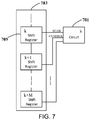
- the display panel further comprises: a gate driving circuit comprising (K+M) stages of shift registers which are cascaded; wherein K is a total number of lines of pixels in the display panel, wherein the scan signal terminal of the circuit in the k-th line is connected to the signal output terminal of the k-th stage shift register, and each of the holding control signal terminals of the circuit in the k-th line is connected to respctive one of the signal output terminals of the (k+1)th to (k+M)th stages of shift registers in one-to-one manner; wherein k is an integer greater than or equal to 1 and less than or equal to K.
- a display device comprising the display panel of any of the embodiments.
- a method of driving a circuit of any of the embodiments comprising: an initialization phase, a data writing phase, a compensation holding phase, and a light emitting phase, wherein the compensation holding phase comprises compensation holding sub-phase(s) corresponding to the respective holding control signal terminal(s) in one-to-one manner; wherein:
- the time for threshold voltage compensation of the driving transistor can be increased, the threshold voltage compensation can be more fully, and the display quality of the image can be improved, in particular, the pixel compensation circuit provided by the embodiment of the present disclosure is applied to the refresh frequency.
- the pixel compensation circuit provided by the embodiment of the present disclosure is applied to the refresh frequency.
- Embodiments of the present disclosure provide a circuit which can be used for pixel compensation. Therefore, in the following, the circuit is sometimes referred to as pixel compensation circuit.
- the circuit may include: a signal control module 1, a compensation control module 2, an initialization module 3, a data writing module 4, a storage module 6, a drive control module 7, and a light emitting device L.
- the circuit can also include a light emission control module 5.
- the data writing module 4 has a control terminal connected to a scan signal terminal Scan, an input terminal connected to a data signal terminal Data, an output terminal connected to a first node A.
- the data writing module 4 is configured for providing the signal at the data signal terminal Data to the first node A under control of the signal at the scan signal terminal Scan.
- the signal control module is configured to provide a control signal to the second node according to the signal at the scan signal terminal and the signals at the respective holding control signal terminals.
- M is a positive integer.
- M 1
- Fig. 1c a case where the signal control module receives a plurality of (M) holding control signal terminals CS_1 to CS_M) is shown as an example.
- the compensation control module 2 has a control terminal connected to the second node B, an input terminal connected to a third node C, and an output terminal connected to a fourth node D.
- the compensation control module 2 is configured to connect the third node C and the fourth node D under control of the signal at/of the second node B.
- the initialization module 3 has a control terminal connected to a reset signal terminal Rst, an input terminal connected to an initialization signal terminal Vinit, and an output terminal connected to the fourth node D.
- the initialization module 3 is configured to provide a signal at the initialization signal terminal Vinit to the fourth node D under control of the signal at the reset signal terminal Rst.
- the drive control module 7 has a control terminal connected to the fourth node D, an input terminal connected to the first node A, and an output terminal connected to the third node C.
- the drive control module 7 is configured to be turned on under control of the signals at the first node A and the fourth node D.
- the storage module 6 is coupled between the fourth node D and a first power terminal ELVDD for maintaining the voltage at the fourth node D stable.
- the capacitance of the transistor (e.g., gate capacitance) connected to the fourth node D can be utilized to provide a feedback to stabilize the voltage; in such a case, the storage module 6 can be omitted.
- the light emission control module 5 has a control terminal connected to a light-emission control signal terminal EM, a first input terminal connected to the first power terminal ELVDD, a second input terminal connected to the third node C, a first output terminal connected to the first node A, and a second output terminal connected to a first end of the light emitting device L. And, a second end of the light emitting device L is connected to a second power terminal ELVSS.
- the light emission control module 5 is configured to cause the drive control module 7 to drive the light emitting device L to emit light, under control of the signal of the light-emission control signal terminal EM.
- a circuit which may include: a signal control module 1, a compensation control module 2, an initialization module 3, a data writing module 4, a drive control module 7, and a light emitting device.
- the data writing module (4) has a control terminal connected to a first signal terminal, an input terminal connected to a data signal terminal, and an output terminal connected to the first node (A).
- the data writing module is configured to provide the signal at/of the data signal terminal to the first node under control of a signal at the first signal terminal.
- a first input terminal of the signal control module (1) is connected to the first signal terminal, a second input terminal thereof is connected to a second signal terminal, and an output terminal thereof is connected to the second node (B).
- the signal control module is configured to provide a control signal to the second node based on a signal of the first signal terminal and signals of the respective second signal terminals.
- a control terminal of the compensation control module (2) is connected to the second node, an input terminal thereof is connected to a third node (C), and an output terminal thereof is connected to a fourth node (D).
- the compensation control module is configured to connect the third node and the fourth node under control of the signal of the second node.
- a control terminal of the initialization module (3) is connected to a reset signal terminal, an input terminal thereof is connected to an initialization signal terminal, and an output terminal thereof is connected to the fourth node (D).
- the initialization module is configured to provide the signal of the initialization signal terminal to the fourth node under control of the signal of the reset signal terminal.
- a control terminal of the drive control module (7) is connected to the fourth node, an input terminal thereof is connected to the first node, and an output terminal is connected to the third node.
- the driving control module is configured to connect the first node and the third node under control of the signals of the first node and the fourth node, to drive the light emitting device.
- the circuit may further include a storage module (6) connected between the fourth node and a first power terminal, for store charges therein.
- the storage module can be used to maintain the voltage at the fourth node D stable.
- the circuit may further include: a light emission control module (5) having a control terminal connected to the light-emission control signal terminal, a first input terminal connected to the first power terminal, a second input terminal connected to the third node, a first output terminal connected to the first node, and a second output terminal connected to a first end of the light emitting device. And a second end of the light emitting device is connected to a second power terminal.
- the light emission control module is configured to allow the drive control module to drive the light emitting device to emit light, under control of the signal of the light-emission control signal terminal.
- a signal control module is provided and cooperats with other modules.
- the threshold voltage compensation time of the driving transistor can be increased, the threshold voltage can be sufficiently compensated, and the image display quality can be improved, especially when applied to a display panel with a high refresh rate.
- the light emitting device may be a light emitting diode, for example, an organic light emitting diode; or the light emitting device may be a quantum dot light emitting diode.
- the present disclosure is not limited thereto; in practical applications, the specific structure of the light emitting device can be designed and determined according to the actual application environment.
- the voltage of the signal at/of the first power terminal is generally a high voltage
- the voltage of the signal at/of the second power terminal is generally a low voltage or ground.
- the disclosure is not limited thereto; in practical applications, the voltages of the signals of the first power terminal and the second power terminal can be determined according to the actual application environment.
- the circuit may further include an anode reset module 8 in order to avoid interference of light-emitting between two adjacent frames.
- a control terminal of the anode reset module 8 is connected to the reset signal terminal Rst, an input terminal thereof is connected to the initialization signal terminal Vinit, and an output terminal thereof is connected to the first end of the light emitting device L.
- the anode reset module 8 is configuured for resetting the first end of the light emitting device L under control of the signal of the reset signal terminal Rst.
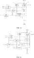
- FIG. 1c is a schematic structural diagram of a circuit according to another embodiment of the present disclosure.
- the structure of the circuit shown in Fig. 1c is substantially the same as that shown in Fig. 1b , except that in Fig. 1c , the signal control module receives a plurality of (M) holding control signal terminals CS_1 to CS_M).
- M control signal terminals
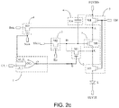
- Each of the first to the M-th input terminals a1_1 ⁇ a1_M of the first AND gate AG1 is connected to a holding control signal terminal CS_m, and the (M+1)th input terminal a1_M+1 of the first AND gate AG1 is connected to the scan signal terminal Scan.
- the output terminal y1 of the first AND gate AG1 is connected to the second node B.
- the first AND gate only outputs high output signals at the ouput terminal thereof when the signals at the first to the (M+1)th input terminals thereof are high potential signals. As long as the signal at one of the input terminals the first to (M+1)th is a low potential signal, a low potential signal is output at the output terminal.
- the first AND gate AG1 is an AND gate with two inputs a1_1 and a1_2.
- the first AND gate is an AND gate having three inputs.
- the first AND gate when the first AND gate has two inputs, as shown in FIG 5 , the first AND gate may include: a first transistor M01, a second transistor M02, a third transistor M03, a fourth transistor M04, afifth transistor M05, and a sixth transistor M06.
- the control electrode of the first transistor M01 serves as a second input terminal a1_2 of the first AND gate, the first pole of the first transistor M01 is connected to a high voltage reference signal terminal VGH, and the second pole of the first transistor M01 is respectively connected to a second pole of the second transistor M02, the control electode of the third transistor M03, the control electode of the fourth transistor M04, and the second pole of the fifth transistor M05.
- the control electode of the second transistor M02 serves as the first input terminal a1_1 of the first AND gate, and the first pole of the second transistor M02 is connected to the high voltage reference signal terminal VGH.
- the first pole of the third transistor M03 is connected to the high voltage reference signal terminal VGH, and the second pole of the third transistor M03 serves as the output terminal y1 of the first AND gate.
- the first pole of the fourth transistor M04 is connected to a low voltage reference signal terminal VGL, and the second pole of the fourth transistor M04 is connected to the second pole of the third transistor M03.
- the control electrode of the fifth transistor M05 is connected to the control electode of the first transistor M01, and the first pole of the fifth transistor M05 is connected to the second pole of the sixth transistor M06.
- the control electode of the sixth transistor M06 is connected to the control electode of the second transistor M02, and the first pole of the sixth transistor M06 is connected to the low voltage reference signal terminal VGL.
- the above is merely illustrative of a structure of the first AND gate having two inputs, and the present disclosure is not limited thereto.
- the specific structure of the first AND gate is not limited to the above-described structure according to the embodiments of the present disclosure, and may be other structures known to those skilled in the art; and the disclosure is not limited thereto.
- the specific structure of the first AND gate can be determined according to the specific application environment, and the disclosure is not limited thereto.
- the specific structure of the first AND gate structures known in the prior art or developed in the future can also be employed, and will not be described herein in detail.
- the scan signal of the next row may be used as the signal at the holding control signal terminal.
- the M holding control signal terminals are defined as the first to the M-th holding control signal terminals
- the signal of the m-th holding control signal terminal is a signal when the signal of the scan signal terminal corresponding to the row which the pixel compensation circuit is located in is shifted by m rows.
- the signal of the first holding control signal terminal is a signal when the signal of the scan signal terminal corresponding to the row, in which the pixel compensation circuit is located, is shifted by one line (row).
- the signal of the first holding control signal terminal is a signal when the signal of the scan signal terminal corresponding to the row, in which the pixel compensation circuit is located, is shifted by one line
- the signal of the second holding control signal terminal is a signal when the signal at the scan signal terminal corresponding to the row, in which the pixel compensation circuit is located, is shifted by 2 lines.
- the signal of the first holding control signal terminal is a signal when the signal of the scan signal terminal corresponding to the row, in which the pixel compensation circuit is located, is shifted by one line
- the signal of the second holding control signal terminal is a signal when the signal at the scan signal terminal corresponding to the row, in which the pixel compensation circuit is located, is shifted by 2 lines
- the signal at the 3rd holding control signal terminal is a signal when the signal of the scan signal terminal corresponding to the row, in which the pixel compensation circuit is located, is shifted by 3 lines.
- Each of the first to the M-th inputs a2_1 to a 2_M of the second AND gate AG2 is connected to a holding control signal terminal CS_m, and the (M+1)th input terminal a2_M+1 of the second AND gate AG2 is connected to the scan signal terminal Scan, and the second output terminal y2 of the AND gate AG2 is connected to the input terminal of the first inverter N1.
- the output of the first inverter N1 is connected to the second node B.
- the second AND gate outputs high potential signal only when the signals of the first to the (M+1)th input terminals are high potential signals. As long as the signal at one of the input terminals 1 to M+1 is a low potential signal, the output terminal outputs a low potential signal.
- the first inverter is used to achieve that the potential of the signal at its output is reverse to the potential of the signal at its input.
- the second AND gate AG1 is an AND gate having two input terminals a2_1 and a2_2.
- the second AND gate is an AND gate having three inputs.
- the structure of the second AND gate may be the same as the structure of the first AND gate.
- the specific structure of the second AND gate can be designed according to the specific application environment, and the present disclosure is not limited to the embodiments disclosed herein.
- a strucutre known in the art or developed in the future can be applied.
- the scan signal of the next row may be used as the signal at the holding control signal terminal.
- the M holding control signal terminals are defined as the first to the M-th holding control signal terminals, and the signal of the m-th holding control signal terminal is a signal when the signal of the scan signal terminal corresponding to the row in which the pixel compensation circuit is located is shifted by m rows.
- the signal of the first holding control signal terminal is a signal when the signal of the scan signal terminal corresponding to the row in which the pixel compensation circuit is located is shifted by one line.
- the signal of the first holding control signal terminal is a signal when the signal of the scan signal terminal corresponding to the row which the pixel compensation circuit is located in is shifted by one line
- the signal of the second holding control signal terminal is a signal when the signal at the scan signal terminal corresponding to the row which the pixel compensation circuit is located in is shifted by 2 lines.
- the signal of the first holding control signal terminal is a signal when the signal of the scan signal terminal corresponding to the row which the pixel compensation circuit is located in is shifted by one line
- the signal of the second holding control signal terminal is a signal when the signal at the scan signal terminal corresponding to the row which the pixel compensation circuit is lcoated in is shifted by 2 lines
- the signal at the 3rd holding control signal terminal is a signal when the signal of the scan signal terminal corresponding to the row which the pixel compensation circuit is lcoated in is shifted by 3 lines.
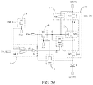
- the signal control module 1 may include : a first OR gate OG1 with M+1 inputs.
- Each of the first to the M-th inputs a3_1 to a3_M of the first OR gate OG1 is connected to a holding control signal terminal CS_m, and the (M+1)th input terminal a3_M+1 of the first OR gate OG1 is connected to the scan signal terminal Scan, the output terminal y3 of the first OR gate OG1 is connected to the second node B.
- FIG. 2e shows such a case where M is a multiple.
- the content described with respect to FIG. 2c can be applied likewise or adaptively to the embodiment shown in FIG. 2e .
- the first OR gate outputs a low potential signal at the output only when the signals of the first to the (M+1)th input terminals are low potential signals. As long as the signal of one of the first to the (M+1)th inputs is a high potential signal, the output terminal outputs a high potential signal.
- the first OR gate OG1 is an OR gate with two inputs a3_1 and a3_2.
- the first OR gate is an OR gate having 3 inputs.
- the specific structure of the first OR gate can be determined according to the specific application environment, and the disclosure shall not be limited thereto.
- the specific structure of the first OR gate can be the same as that of the prior art, and will be readily understood by those skilled in the art, and thus further details are omitted herein from being described.
- the scan signal of the next row may be used as the signal at the holding control signal terminal.
- the M holding control signal terminals are defined as the first to the M-th holding control signal terminal, and the signal of the m-th holding control signal terminal is a signal when the signal of the scan signal terminal corresponding to the row which the pixel compensation circuit is located in is shifted by m rows.
- the signal of the first holding control signal terminal is a signal when the signal of the scan signal terminal corresponding to the row which the pixel compensation circuit is located in is shifted by one line.
- the signal of the first holding control signal terminal is a signal when the signal of the scan signal terminal corresponding to the row which the pixel compensation circuit is located in is shifted by one line
- the signal of the second holding control signal terminal is a signal when the signal at the scan signal terminal corresponding to the row which the pixel compensation circuit is located in is shifted by 2 lines.
- the signal of the first holding control signal terminal is a signal when the signal of the scan signal terminal corresponding to the row which the pixel compensation circuit is located in is shifted by one line
- the signal of the second holding control signal terminal is a singal when the signal at the scan signal terminal corresponding to the row which the pixel compensation circuit is located in is shifted by 2 lines
- the signal at the 3rd holding control signal terminal is a signal when the signal of the scan signal terminal corresponding to the row which the pixel compensation circuit is located in is shifted by 3 lines.
- the signal control module 1 may include: a second inverter N2, and a second OR gate OG2 having M+1 inputs.
- Each of the first to the M-th inputs a4_1 to a4_M of the second OR gate OG2 is connected to a respective holding control signal terminal CS_m, and the (M+1)th input terminal a4_M+1 of the second OR gate OG2 is connected to the scan signal terminal Scan, and a output terminal y4 of the second OR gate OG2 is connected to the input terminal of the second inverter N2.
- the output of the second inverter N2 is connected to the second node B.
- the second OR gate outputs a low potential signal at the output thereof only when the signals of the first to the (M+1)th input terminals are low potential signals. As long as the signal of one of the first to the (M+1)th inputs is a high potential signal, the output terminal outputs a high potential signal.
- the second inverter is used to make the potential of the signal at its output reversed repective to the potential of the signal at its input.
- M 1, that is, there is one holding control signal terminal CS_1
- the second OR gate may be an OR gate with two inputs a4_1 and a4_2.
- M 2, that is, there are 2 holding control signal terminals
- the second OR gate is an OR gate having 3 inputs.
- the structure of the second OR gate may be the same as the structure of the first OR gate.
- the specific structure of the second OR gate can be designed according to a specific application environment; The present disclosure is not limited thereto.
- the specific structure of the second or the second gate can be the same as that of the prior art, and will readily be understood by those skilled in the art, and thus further details are not described herein.
- the scan signal of the next row may be used as the signal of the holding control signal terminal.
- the M holding control signal terminals are defined as the first to the M-th holding control signal terminals, and the signal of the m-th holding control signal terminal is a signal when the signal of the scan signal terminal corresponding to the row which the pixel compensation circuit is located in is shifted by m rows.
- the signal of the first holding control signal terminal is a signal when the signal of the scan signal terminal corresponding to the row which the pixel compensation circuit is located in is shifted by one line.
- the signal of the first holding control signal terminal is a signal when the signal of the scan signal terminal corresponding to the row which the pixel compensation circuit is located in is shifted by one line
- the signal of the second holding control signal terminal is a signal when the signal at the scan signal terminal corresponding to the row which the pixel compensation circuit is located in is shifted by 2 lines.
- the signal of the first holding control signal terminal is a signal when the signal of the scan signal terminal corresponding to the row which the pixel compensation circuit is located in is shifted by one line
- the signal of the second holding control signal terminal is a signal when the signal at the scan signal terminal corresponding to the row which the pixel compensation circuit is located in is shifted by 2 lines
- the signal at the 3rd holding control signal terminal is a signal when the signal of the scan signal terminal corresponding to the row which the pixel compensation circuit is located in is shifted by 3 lines.
- the driving control module 7 may include: a driving transistor M0; wherein the driving transistor M0 has a control electrode connected to the fourth node D is, a first pole connected to the first node A, and a second pole connected to the third node C.
- the driving transistor M0 may be a P-type transistor; wherein the control electrode of the driving transistor M0 is its gate. The first pole of the transistor M0 is its source, and the second pole of the transistor M0 is its drain.
- the driving transistor may also be an N-type transistor; wherein the control electrode of the driving transistor is its gate, the first pole of the driving transistor is its drain, and the second pole of the driving transistor is its source.
- the specific type of the driving transistor can be determined according to the actual application environment, and the disclosure is not limited thereto.
- the compensation control module 2 may include: a first switching transistor M1; wherein, the control elelctrode of the first switching transistor M1 is connected to the second node B, the first pole of the first switching transistor M1 is connected to the third node C, and the second pole of the first switching transistor M1 is connected to the fourth node D.
- the first switching transistor M1 may be a P-type transistor.
- the first switching transistor M1 may also be an N-type transistor. And the disclosure is not limited thereto.
- the third node and the fourth node when the first switching transistor is in an ON state under control of the signal of the second node, the third node and the fourth node can be connected. That is, the control electrode of the driving transistor is connected to the second pole thereof.
- the initialization module 3 may include: a second switching transistor M2; wherein, the control electrode of the second switching transistor M2 is connected to the reset signal terminal Rst, the first pole of the second switching transistor M2 is connected to the initialization signal terminal Vinit, and the second pole of the second switching transistor M2 is connected to the fourth node D.
- the second switching transistor M2 may be a P-type transistor.
- the second switching transistor M2 may also be an N-type transistor; and the disclosure is not limited thereto.
- the signal of the initialization signal terminal can be provided to the fourth node to initialize the control electrode of the drive transistor.
- the data writing module 4 may include: a third switching transistor M3; wherein, the control electrode of the third switching transistor M3 is connected to the scan signal terminal Scan, the first pole of the third switching transistor M3 is connected to the data signal terminal Data, and the second pole of the third switching transistor M3 is connected to the first node A.
- the third switching transistor M3 may be a P-type transistor.
- the third switching transistor M3 may be an N-type transistor; and the disclosure is not limited thereto.
- the signal of the data signal terminal can be provided to the first node.
- the light emission control module 5 may include: a fourth switching transistor M4 and a fifth switching transistor M5; wherein the control electrode of the fourth switching transistor M4 is connected to the light-emission control signal terminal EM, the first pole of the fourth switching transistor M4 is connected to the first power terminal ELVDD, and the second pole of the fourth switching transistor M4 is connected to the first node A.
- the control electrode of the fifth switching transistor M5 is connected to the light-emission control signal terminal EM, the first pole of the fifth switching transistor M5 is connected to the third node C, and the second pole of the fifth switching transistor M5 is connected to the first end of the light emitting device L.
- the fourth switching transistor M4 and the fifth switching transistor M5 may be P-type transistors.
- the fourth switching transistor M4 and the fifth switching transistor M5 may be N-type transistors; and the disclosure is not limited thereto.
- the signal of the first power terminal can be provided to the first node.
- the signal of the third node can be provided to the first end of the light emitting device, that is, the operate current generated by the driving transistor for driving the light emitting device to emit light is applied to the light emitting device so that the driving transistor drives the light emitting device to emit light.
- the anode reset module 8 may include: a sixth switching transistor M6; wherein, the control electrode of the sixth switching transistor M6 is connected to the reset signal terminal Rst, the first pole of the sixth switching transistor M6 is connected to the initialization signal terminal Vinit, and the second pole of the sixth switching transistor M6 is connected to the first end of the light emitting device L.
- the sixth switching transistor M6 may be a P-type transistor.
- the sixth switching transistor M6 may be an N-type transistor. And the present disclosure is not limited thereto.
- the signal of the initialization signal terminal may be provided to the first end of the light emitting device to reset the light-emitting device so as to avoid interference between the light emittings of adjacent frames.
- the storage module 6 may include: a storage capacitor Cst; wherein the first end of the storage capacitor Cst is connected to the fourth node D, and the second end of the storage capacitor Cst is connected to the first power terminal ELVDD.
- the storage capacitor may be charged or discharged under control of the signals of the first power terminal and the fourth node, and when the fourth node is in a floating state, due to the bootstrap action of the storage capacitor, the voltage difference between the two ends thereof can be kept stable, that is, the voltage difference between the first power terminal and the fourth node can be kept stable.
- the foregoing is only for exemplifying some specific structures of the modules in the pixel compensation circuit according to the embodiments of the present disclosure.
- the specific structures of the modules are not limited to the above-mentioned structures according to the embodiment of the present disclosure, and the present disclosure is not limited thereto.
- Other structures known to the skilled person in the field may also be applied,.
- the first to sixth switching transistors M1 to M6 may all be P-type transistors.
- the first to sixth switching transistors M1 to M6 may also all be N-type transistors. The present disclosure is not limited thereto.
- the P-type transistor is turned off under the action of the high-potential gate signal, and is turned on under the action of the low-potential gate signal;
- the N-type transistor is turned on under the action of the high-potential gate signal and turned off under the action of the low-potential gate signal.
- the transistors may be thin film transistors (TFT) or metal oxide semiconductor field effect transistor (MOS, Metal-Oxide- Semiconductor); however, the present disclosure shall not be limited thereto.
- the control electrodes of the transistors are gates, and the first poles thereof can be used as sources and the second poles can be used as drains, or vice versa, according to the types of the transistors and the signals at the signal terminals.
- the present disclosure is not limited thereto. In the specific embodiments as above, the description is made and exemplified with MOS transistors.
- FIG. 4a the corresponding input timing diagram is shown in FIG. 4a .
- the compensation holding phase T3 includes one compensation holding sub-phase.
- B1 represents the signal of the second node B.
- both the second switching transistor M2 and the sixth switching transistor M6 are turned on.
- the turned-on second switching transistor M2 supplies the signal of the initialization signal terminal Vinit to the fourth node D, that is, the control electrode of the driving transistor M0, to initialize the control electrode of the driving transistor M0.
- the voltage of the control electrode of the driving transistor M0 is the voltage Vinit of the signal of the initialization signal terminal Vinit.
- the turned-on sixth switching transistor M6 supplies a signal of the initialization signal terminal Vinit to the first end of the light emitting device L to reset the light emitting device L.
- the turned-on first switching transistor M1 connects the control electrode of the driving transistor M0 and the second pole thereof, so that the driving transistor M0 is in a diode-connected state, thus the voltage V data input to the first node A charges the storage capacitor Cst via the driving transistor M0.
- the turned-on first switching transistor M1 connects the control electrode of the driving transistor M0 and the second pole thereof, so that the driving transistor M0 is in a diode-connected state, thus the voltage V data input to the first node A continues to charge the storage capacitor Cst through the driving transistor M0 until the voltage of the fourth node D becomes: V data -
- the voltage of the fourth node D is kept stable by the storage capacitor Cst.
- the turned-on fourth switching transistor M4 supplies the signal of the first power terminal ELVDD to the first node A, so that the voltage of the first node A becomes the voltage V dd of the signal of the first power terminal ELVDD, that is, the voltage of the first pole of the driving transistor M0 beomces V dd .
- the voltage of the fourth node D is maintained as: V data -
- the operating current I L formula that the operating current I L outputted by the driving transistor M0 for driving the light-emitting device L to emit light is only related to the voltage V dd of the first power terminal ELVDD and the voltage V data of the data signal terminal Data, and regardless of the threshold voltage V th of the driving transistor M0.
- the problem of the threshold voltage V th drift due to the process of the driving transistor M0 and the long-time operation can be solved.
- the first AND gate AG1 is provided so that the control electrode of the driving transistor M0 and the second pole can be connected in the data writing phase T2 and the compensation holding phase T3, so that the voltage at the first node A charges the fourth node D through the driving transistor M0 to completely write V th to the fourth node D. Therefore, compared with the convential solution in which V th is written only in the data writing phase T2, since the V th is written not only in the data writing phase T2 but also continuously written in the compensation holding phase T3 before the light emitting phase T4.
- the V th compensation time is extended to make the V th compensation more sufficient, and thus when the pixel compensation circuit according to the embodiments of the present disclosure is applied to the display panel, especially when applied to a display panel with a high refresh rate, the image display performance of the display panel can be improved.
- FIG. 4a the corresponding input timing chart is shown in FIG. 4a .
- the compensation holding phase T3 includes one compensation holding sub-phase.
- B2 represents the signal of the second node B.
- the second AND gate AG2 outputs a low potential signal to the first inverter N1, so that the first inverter N1 outputs a high potential signal to the second node B to control the first switching transistor M1 to be turned on.
- the turned-on first switching transistor M1 connects the control electrode of the driving transistor M0 and the second pole thereof, so that the driving transistor M0 is in a diode-connected state, thus the voltage V data input to the first node A charges the storage capacitor Cst through the driving transistor M0.
- the turned-on first switching transistor M1 connects the control electrode of the driving transistor M0 and the second pole thereof, so that the driving transistor M0 is in a diode-connected state, so that the voltage V data input to the first node A continues to charge the storage capacitor Cst through the driving transistor M0 until the voltage of the fourth node D becomes: V data -
- the voltage of the fourth node D is kept stable by the storage capacitor Cst.
- the turned-on fourth switching transistor M4 supplies the signal of the first power terminal ELVDD to the first node A, so that the voltage of the first node A becomes the voltage V dd of the signal of the first power terminal ELVDD, that is, the voltage of the first pole of the driving transistor M0becomes V dd .
- the voltage of the fourth node D is maintained at: V data -
- the operating current I L formula that the operating current I L outputted by the driving transistor M0 for driving the light-emitting device L to emit light is only related to the voltage V dd of the first power terminal ELVDD and the voltage V data of the data signal terminal Data, and regardless of the threshold voltage V th of the driving transistor M0.
- the problem of the threshold voltage V th drifting due to the process of the driving transistor M0 and the long-time operation can be solved.
- the control electrode and the second pole of the driving transistor M0 can be connected in both the data writing phase T2 and the compensation holding phase T3 by the second AND gate AG2 and the first inverter N1.
- the voltage of the first node A charges the fourth node D through the driving transistor M0 to completely write V th to the fourth node D. Therefore, compared with the conventional solution in which V th is written only in the data writing phase T2, since the V th is written not only in the data writing phase T2, but also continuously written in the compensation holding phase T3 before the light emitting phase T4, the V th compensation time is extended to make the V th compensation more sufficient.
- the pixel compensation circuit according to the embodiments of the present disclosure is applied to the display panel, especially when applied to a display panel with a high refresh rate, the image display performance of the display panel can be improved.
- FIG. 4b the corresponding input timing chart is shown in FIG. 4b .
- the compensation holding phase T3 includes one compensation holding sub-phase.
- B3 represents the signal of the second node B.
- the turned-on first switching transistor M1 connects the control electrode of the driving transistor M0 and the second pole thereof, so that the driving transistor M0 is in a diode-connected state, thus the voltage V data input to the first node A charges the storage capacitor Cst through the driving transistor M0.
- the turned-on first switching transistor M1 connects the control electrode of the driving transistor M0 and the second pole thereof, so that the driving transistor M0 is in a diode-connected state, thus the voltage V data input to the first node A continues to charge the storage capacitor Cst through the driving transistor M0 until the voltage of the fourth node D becomes: V data -
- the voltage of the fourth node D is kept stable by the storage capacitor Cst.
- the turned-on fourth switching transistor M4 supplies the signal of the first power terminal ELVDD to the first node A, so that the voltage of the first node A becomes the voltage V dd of the signal of the first power terminal ELVDD, that is, the voltage of the first pole of the driving transistor M0 becomes V dd .
- the voltage of the fourth node D is maintained as: V data -
- the operating current I L formula that the operating current I L outputted by the driving transistor M0 for driving the light-emitting device L to emit light is only related to the voltage V dd of the first power terminal ELVDD and the voltage V data of the data signal terminal Data, and regardless of the threshold voltage V th of the driving transistor M0.
- the problem of the threshold voltage V th drifting due to the process of the driving transistor M0 and the long-time operation can be solved.
- the control electrode and the second pole of the driving transistor M0 can be connected in the data writing phase T2 and the compensation holding phase T3 by providing the first OR gate OG1, so that the voltage of the first node A charges the fourth node D through the driving transistor M0 to completely write V th to the fourth node D. Therefore, compared with the conventional solution in which V th is written only in the data writing phase T2, since the V th is written not only in the data writing phase T2, but also continuously written in the compensation holding phase T3 before the light emitting phase T4, the V th compensation time is extended to make the V th compensation more sufficient.
- the pixel compensation circuit according to the embodiments of the present disclosure is applied to the display panel, especially when applied to a display panel with a high refresh rate, and the image display performance of the display panel can be improved.
- FIG. 4b the corresponding input timing chart is shown in FIG. 4b .
- the compensation holding phase T3 includes one compensation holding sub-phase.
- B4 represents the signal of the second node B.
- the second OR gate OG2 outputs a high potential signal to the second inverter N2, so that the second inverter outputs a low potential signal to the second node B to control the first switching transistor M1 to be turned on.
- the turned-on first switching transistor M1 connects the control electrode of the driving transistor M0 and the second pole thereof, so that the driving transistor M0 is in a diode-connected state, thus the voltage V data input to the first node A charges the storage capacitor Cst through the driving transistor M0.
- the turned-on first switching transistor M1 connects the control electrode of the driving transistor M0 and the second pole thereof, so that the driving transistor M0 is in a diode-connected state, thus the voltage V data input to the first node A continues to charge the storage capacitor Cst through the driving transistor M0 until the voltage of the fourth node D becomes: V data -
- the voltage of the fourth node D is kept stable by the storage capacitor Cst.
- the turned-on fourth switching transistor M4 supplies the signal of the first power terminal ELVDD to the first node A, so that the voltage of the first node A becomes the voltage V dd of the signal of the first power terminal ELVDD, that is, the voltage of the first pole of the driving transistor M0 becomes V dd .
- the voltage of the fourth node D is maintained as: V data -
- the operating current I L formula that the operating current I L outputted by the driving transistor M0 for driving the light-emitting device L to emit light is only related to the voltage V dd of the first power terminal ELVDD and the voltage V data of the data signal terminal Data, and regardless of the threshold voltage V th of the driving transistor M0.
- the problem of the threshold voltage V th drifting due to the process of the driving transistor M0 and the long-time operation can be solved.
- the control electrode and the second pole of the driving transistor M0 can be connected in both the data writing phase T2 and the compensation holding phase T3 by providing the second OR gate OG2 and the second inverter N2, so that the voltage of the first node A charges the fourth node D through the driving transistor M0 to completely write V th to the fourth node D. Therefore, compared with conventional solution in which V th is written only in the data writing phase T2, since the V th is written not only in the data writing phase T2 but also continuously written in the compensation holding phase T3 before the light emitting phase T4, the V th compensation time is extended to make the V th compensation more sufficient.
- the pixel compensation circuit according to the embodiments of the present disclosure is applied to the display panel, especially when applied to a display panel with a high refresh rate, the image display performance of the display panel can be improved.
- the embodiment of the present disclosure further provides a driving method of the pixel compensation circuits according to the embodiments of the present disclosure.
- the method includes: an initialization phase, a data writing phase, a compensation holding phase, and a light emitting phase;
- the compensation hold phase includes compensation holding sub-phase(s) corresponding to the respective holding control signal terminal(s).
- Step S601 In the initialization phase, a first potential signal is provided to the reset signal terminal, and a second potential signal is respectively provided to the scan signal terminal, the respective holding control signal terminal(s), and the light-emission control signal terminal.
- Step S602 In the data writing phase, a first potential signal is provided to the scan signal terminal, and a second potential signal is respectively provided to the reset signal terminal, the respective holding control signal terminal(s), and the light-emission control signal terminal.
- Step S603 In the compensation holding phase, for each compensation holding sub-phase, a first potential signal is provided to the holding control signal terminal corresponding to the compensation holding sub-stage, and a second potential signal is provided to the other holding control signal terminals than the holding control signal terminal corresponding to the compensation holding sub-stage, the reset signal terminal, the scan signal terminal, and the light-emission control signal terminal respectively.
- Step S604 In the light emission phase, a first potential signal is provided to the light emission control signal terminal, and a second potential signal is respectively provided to the reset signal terminal, the scan signal terminal, and the respective holding control signal terminal(s).
- the above-mentioned driving method according to the embodiment of the present disclosure can improve the time for the threshold voltage compensation of the driving transistor, and make the threshold voltage compensation more sufficient.
- the pixel compensation circuit according to the embodiments of the present disclosure is applied to the display panel with high refresh frequency, the imagedisplay quality can be improved.
- the first potential signal may be a high potential signal, and correspondingly, the second potential signal is a low potential signal.
- the first potential signal may be a low potential signal, and correspondingly, the second potential signal is a high potential signal. This can be determined depending on whether the switching transistor in the pixel compensation circuit is an N-type transistor or a P-type transistor. The present disclosure is not limited thereto.
- a display panel including the circuit according to any of the embodiments of the present disclosure.
- the above display panel according to the embodiment of the present disclosure may be an organic light emitting display panel.
- a gate drive circuit in the display panel a gate drive circuit can be employed to output a scan signal.
- the display panel may further include: a gate driving circuit comprising cascaded (K+M) stages of shift registers; wherein K is a total number of rows of pixels in the display panel.
- FIG. 7 illustrates a structural diagram of a circuit in a display panel according to an embodiment of the present disclosure.
- a circuit 701 and a gate drive circuit 703 in the k-th row are schematically shown in FIG. 7 .
- the circuit 701 can be a circuit for pixel compensation in accordance with any of the above-mentioned embodiments.
- the gate drive circuit 703 can include K+M stages of shift registers which are cascaded.
- the shift registers k-th to (k+M)th associated with the circuit 701 in the k-th row are schematically shown in FIG.
- k is an integer greater than or equal to 1 and less than or equal to K.
- the scan signal terminal (SCAN) of the pixel compensation circuit in the k-th row is connected to the signal output terminal of the k-th stage shift register.
- the holding control signal terminals (CONTROL) of the pixel compensation circuit in the k-th row are connected to the signal output terminals of the (k+1)th to (k+M)th stage shift registers in a one-to-one manner.
- the display panel includes: a gate driving circuit comprising cascaded K+1 stages of shift registers; wherein, the scan signal terminal of the pixel compensation circuit in the k-th row is connected to the signal output terminal of the k-th stage shift register, and the holding control signal terminal of the pixel compensation circuit in the k-th row is correspondingly connected to the signal output terminal of the (k+1)th stage shift register.
- M 1.
- the display panel includes: a gate driving circuit comprising cascaded K+1 stages of shift registers; wherein, the scan signal terminal of the pixel compensation circuit in the k-th row is connected to the signal output terminal of the k-th stage shift register, and the holding control signal terminal of the pixel compensation circuit in the k-th row is correspondingly connected to the signal output terminal of the (k+1)th stage shift register.
- M 1.
- the display panel includes: a gate driving circuit comprising cascaded K+1 stages of shift registers; wherein, the scan signal terminal of the pixel compensation circuit in the k-th
- the display panel includes: a gate driving circuit comprising cascaded K+2 stages of shift registers; wherein, the scan signal terminal of the pixel compensation circuit in the k-th row is connected to the signal output terminal of the k-th stage shift register, and one of the holding control signal terminals of the pixel compensation circuit in the k-th row is connected to the signal output terminal of the (k+1)th stage shift register, and the other holding control signal terminal is connected to the signal output terminals of the (k+2)th stage shift register.
- M 3
- the display panel includes: a gate driving circuit comprising cascaded K+3 stages of shift registers; wherein, the scan signal terminal of the pixel compensation circuit in the k-th row is connected to the signal output terminal of the k-th stage shift register, the first holding control signal terminal of the pixel compensation circuit in the k-th row is connected to the signal output terminal of the (k+1)th stage shift register, the second holding control signal terminal thereof is connected to the signal output terminal of the (k+2)th stage shift register, and the third holding control signal terminal thereof is connected to the signal output terminal of the (k+3)th stage shift register.
- M 4, 5, 6..., and it will not be repeatedly described here.
- the specific structure of the shift register may employ a structure known in the art or developed in the future, which is thus not described herein in detail and shall not be construed as limiting the present disclosure.
- the (K+1)th to (K+M)th stages of shift registers may be not used to input signals to the scan signal terminals in the pixel compensation circuit of the display panel, instead they can be used only for inputting signals to the holding control signal terminals.
- the specific settings of the (K+1)th to (K+M)th stages of shift registers can be determined according to the actual application environment.
- a display device including the above display panel according to the embodiments of the present disclosure.
- the display device may comprise any product or component having display function, such as mobile phone, tablet computer, television, display, notebook computer, digital photo frame, navigator, and the like.
- display function such as mobile phone, tablet computer, television, display, notebook computer, digital photo frame, navigator, and the like.
- display device may comprise any product or component having display function, such as mobile phone, tablet computer, television, display, notebook computer, digital photo frame, navigator, and the like.
- display function such as mobile phone, tablet computer, television, display, notebook computer, digital photo frame, navigator, and the like.
- the pixel compensation circuits, the driving methods thereof, the display panels and the display devices may include: a signal control module, a compensation control module, an initialization module, a data writing module, a light emission control module, a storage module, a drive control module, and a light-emitting device; wherein the data writing module is configured to provide the signal of the data signal terminal to the first node under control of the signal of the scan signal terminal; the signal control module is configured to combine the signal of the scan signal terminal with the signal of the respective holding control signal terminal(s) and provide the combined signal to the second node; the compensation control module is configured to connect the third node and the fourth node under control of the signal of the second node; the initialization module is configured to provide the signal of the initialization signal terminal to the fourth node under control of the signal of the reset signal terminal; the driving control module is configured to be turned on under control of the signals of the first node and the fourth node; the storage module is configured to maintain the voltage of the fourth node stable
- the time for threshold voltage compensation for the driving transistor can be increased to make the threshold voltage compensation more sufficient, so that the image display quality can be improved, particularly when they are applied to a display panel having a high refresh rate.
Landscapes
- Engineering & Computer Science (AREA)
- Physics & Mathematics (AREA)
- Computer Hardware Design (AREA)
- General Physics & Mathematics (AREA)
- Theoretical Computer Science (AREA)
- Control Of Indicators Other Than Cathode Ray Tubes (AREA)
- Control Of El Displays (AREA)
Applications Claiming Priority (2)
| Application Number | Priority Date | Filing Date | Title |
|---|---|---|---|
| CN201710734919.7A CN107331351B (zh) | 2017-08-24 | 2017-08-24 | 一种像素补偿电路、其驱动方法、显示面板及显示装置 |
| PCT/CN2018/086729 WO2019037476A1 (fr) | 2017-08-24 | 2018-05-14 | Circuit de compensation de pixel, son procédé d'attaque, panneau d'affichage et dispositif d'affichage |
Publications (2)
| Publication Number | Publication Date |
|---|---|
| EP3675101A1 true EP3675101A1 (fr) | 2020-07-01 |
| EP3675101A4 EP3675101A4 (fr) | 2021-04-21 |
Family
ID=60228263
Family Applications (1)
| Application Number | Title | Priority Date | Filing Date |
|---|---|---|---|
| EP18830708.6A Withdrawn EP3675101A4 (fr) | 2017-08-24 | 2018-05-14 | Circuit de compensation de pixel, son procédé d'attaque, panneau d'affichage et dispositif d'affichage |
Country Status (4)
| Country | Link |
|---|---|
| US (1) | US11176886B2 (fr) |
| EP (1) | EP3675101A4 (fr) |
| CN (1) | CN107331351B (fr) |
| WO (1) | WO2019037476A1 (fr) |
Families Citing this family (20)
| Publication number | Priority date | Publication date | Assignee | Title |
|---|---|---|---|---|
| CN107331351B (zh) * | 2017-08-24 | 2023-08-29 | 京东方科技集团股份有限公司 | 一种像素补偿电路、其驱动方法、显示面板及显示装置 |
| CN107808630B (zh) * | 2017-12-01 | 2023-09-12 | 京东方科技集团股份有限公司 | 一种像素补偿电路、其驱动方法、显示面板及显示装置 |
| CN108154844B (zh) * | 2018-03-09 | 2019-07-30 | 京东方科技集团股份有限公司 | 一种像素电路、其驱动方法及显示面板 |
| CN108598121B (zh) * | 2018-04-27 | 2020-06-05 | 京东方科技集团股份有限公司 | 一种双面显示基板及其制作方法、驱动电路及其驱动方法 |
| CN208335702U (zh) * | 2018-05-14 | 2019-01-04 | 北京京东方技术开发有限公司 | 显示面板及显示装置 |
| CN110867160B (zh) * | 2018-08-27 | 2021-05-11 | 上海和辉光电股份有限公司 | 一种像素电路及其驱动方法和显示面板 |
| CN109523951A (zh) * | 2018-12-29 | 2019-03-26 | 云谷(固安)科技有限公司 | 一种像素电路和显示装置 |
| CN111445851B (zh) | 2020-04-30 | 2021-10-08 | 京东方科技集团股份有限公司 | 像素电路及其驱动方法、显示装置 |
| CN113223458B (zh) * | 2021-01-25 | 2023-01-31 | 重庆京东方显示技术有限公司 | 一种像素电路及其驱动方法、显示基板和显示装置 |
| GB2615936A (en) * | 2021-04-23 | 2023-08-23 | Boe Technology Group Co Ltd | Pixel circuit and driving method therefor, and display device |
| CN114241977B (zh) * | 2021-12-17 | 2024-07-19 | 昆山国显光电有限公司 | 像素电路及其驱动方法和显示面板 |
| CN114420069B (zh) * | 2022-02-16 | 2023-06-02 | 武汉京东方光电科技有限公司 | 移位寄存器单元及显示面板 |
| WO2023178654A1 (fr) * | 2022-03-25 | 2023-09-28 | 京东方科技集团股份有限公司 | Circuit de pixels, procédé d'attaque de pixels et appareil d'affichage |
| CN114822358B (zh) * | 2022-04-29 | 2025-07-15 | 上海天马微电子有限公司 | 一种显示面板和显示装置 |
| CN114863879B (zh) * | 2022-05-23 | 2023-05-02 | 惠科股份有限公司 | 有机发光二极管控制电路及显示面板 |
| CN115294923B (zh) * | 2022-08-29 | 2023-11-21 | 惠科股份有限公司 | 稳压电路及显示面板 |
| CN115775538B (zh) * | 2022-11-24 | 2025-08-19 | 北京小米移动软件有限公司 | 像素驱动电路、显示面板及终端 |
| CN116229888A (zh) * | 2023-03-03 | 2023-06-06 | 武汉天马微电子有限公司 | 像素电路、显示面板及显示装置 |
| CN116092430A (zh) * | 2023-03-20 | 2023-05-09 | 惠科股份有限公司 | 像素驱动电路、时序控制方法和显示面板 |
| CN118155545A (zh) * | 2024-04-02 | 2024-06-07 | 武汉华星光电半导体显示技术有限公司 | 像素电路及显示面板 |
Family Cites Families (20)
| Publication number | Priority date | Publication date | Assignee | Title |
|---|---|---|---|---|
| US7616177B2 (en) * | 2004-08-02 | 2009-11-10 | Tpo Displays Corp. | Pixel driving circuit with threshold voltage compensation |
| KR100658297B1 (ko) * | 2004-10-13 | 2006-12-14 | 삼성에스디아이 주식회사 | 화소와 이를 가지는 발광 표시장치 및 그의 구동방법 |
| KR100645700B1 (ko) * | 2005-04-28 | 2006-11-14 | 삼성에스디아이 주식회사 | 주사 구동부 및 이를 이용한 발광 표시장치와 그의 구동방법 |
| JP5160748B2 (ja) * | 2005-11-09 | 2013-03-13 | 三星ディスプレイ株式會社 | 発光表示装置 |
| TWI371018B (en) | 2006-05-09 | 2012-08-21 | Chimei Innolux Corp | System for displaying image and driving display element method |
| KR100807062B1 (ko) * | 2007-04-06 | 2008-02-25 | 삼성에스디아이 주식회사 | 유기 전계 발광 표시 장치 |
| KR101125571B1 (ko) * | 2010-02-05 | 2012-03-22 | 삼성모바일디스플레이주식회사 | 화소, 이를 이용한 표시 장치 및 그 구동 방법 |
| TWI471843B (zh) * | 2012-07-18 | 2015-02-01 | Innocom Tech Shenzhen Co Ltd | 有機發光二極體像素電路與顯示器 |
| US9947266B2 (en) * | 2012-12-19 | 2018-04-17 | Sharp Kabushiki Kaisha | Drive circuit, display device and driving method |
| KR102090189B1 (ko) * | 2013-11-04 | 2020-04-16 | 삼성디스플레이 주식회사 | 유기전계발광 표시장치와 그 구동방법 |
| CN103927982B (zh) * | 2014-03-24 | 2016-08-17 | 京东方科技集团股份有限公司 | 像素电路及其驱动方法、显示装置 |
| TWI533277B (zh) * | 2014-09-24 | 2016-05-11 | 友達光電股份有限公司 | 有機發光二極體畫素電路 |
| CN104409051A (zh) * | 2014-12-24 | 2015-03-11 | 京东方科技集团股份有限公司 | 一种像素电路、有机电致发光显示面板及显示装置 |
| KR102307500B1 (ko) * | 2015-03-20 | 2021-10-01 | 삼성디스플레이 주식회사 | 표시 장치의 화소회로 및 이를 포함하는 표시 장치 |
| CN104835452B (zh) | 2015-05-28 | 2017-04-19 | 京东方科技集团股份有限公司 | 一种像素电路、其驱动方法及相关装置 |
| CN105185305A (zh) * | 2015-09-10 | 2015-12-23 | 京东方科技集团股份有限公司 | 一种像素电路、其驱动方法及相关装置 |
| CN106097976B (zh) * | 2016-08-23 | 2019-03-12 | 上海天马微电子有限公司 | 像素驱动电路及显示装置 |
| CN106486063A (zh) * | 2016-10-26 | 2017-03-08 | 京东方科技集团股份有限公司 | 像素驱动电路及其驱动方法、显示面板和显示装置 |
| CN207337880U (zh) * | 2017-08-24 | 2018-05-08 | 京东方科技集团股份有限公司 | 一种像素补偿电路、显示面板及显示装置 |
| CN107331351B (zh) * | 2017-08-24 | 2023-08-29 | 京东方科技集团股份有限公司 | 一种像素补偿电路、其驱动方法、显示面板及显示装置 |
-
2017
- 2017-08-24 CN CN201710734919.7A patent/CN107331351B/zh active Active
-
2018
- 2018-05-14 WO PCT/CN2018/086729 patent/WO2019037476A1/fr not_active Ceased
- 2018-05-14 EP EP18830708.6A patent/EP3675101A4/fr not_active Withdrawn
- 2018-05-14 US US16/319,185 patent/US11176886B2/en not_active Expired - Fee Related
Also Published As
| Publication number | Publication date |
|---|---|
| US20200388217A1 (en) | 2020-12-10 |
| EP3675101A4 (fr) | 2021-04-21 |
| WO2019037476A1 (fr) | 2019-02-28 |
| CN107331351A (zh) | 2017-11-07 |
| CN107331351B (zh) | 2023-08-29 |
| US11176886B2 (en) | 2021-11-16 |
Similar Documents
| Publication | Publication Date | Title |
|---|---|---|
| EP3675101A1 (fr) | Circuit de compensation de pixel, son procédé d'attaque, panneau d'affichage et dispositif d'affichage | |
| US11393373B2 (en) | Gate drive circuit and drive method thereof, display device and control method thereof | |
| US10504438B2 (en) | Pixel circuit and driving method thereof, display panel | |
| US10679564B2 (en) | Shift register and display apparatus including the same | |
| US10565933B2 (en) | Pixel circuit, driving method thereof, array substrate, display device | |
| US10685616B2 (en) | Shift register circuit, method for driving the same, gate drive circuit, and display panel | |
| US9865211B2 (en) | Shift register unit, gate driving circuit and display device | |
| US11869429B2 (en) | Display panel and driving method therefor, and display device | |
| US10032416B2 (en) | GOA unit, Goa circuit, display driving circuit and display device | |
| US20210056880A1 (en) | Shift register unit and method for driving same, gate drive circuit, and display device | |
| US9087480B2 (en) | Scan lines driver and organic light emmiting display device using the same | |
| US20180122289A1 (en) | Shift register, driving method, gate driving circuit and display device | |
| US10714010B2 (en) | Pixel compensation circuit, method for driving the same, organic light-emitting diode display panel, and display device | |
| JP4321266B2 (ja) | インバータ回路および表示装置 | |
| US11107381B2 (en) | Shift register and method for driving the same, gate driving circuit and display device | |
| US11217148B2 (en) | Shift register unit, driving method, gate driver on array and display device | |
| CN108470544B (zh) | 一种像素驱动电路及其驱动方法、阵列基板和显示装置 | |
| US20210335237A1 (en) | Pixel Driving Circuit and Method, Display Apparatus | |
| US12300177B2 (en) | Display panel and display device | |
| CN114023264B (zh) | 驱动电路、驱动模组、驱动方法和显示装置 | |
| CN207337880U (zh) | 一种像素补偿电路、显示面板及显示装置 | |
| US10109234B2 (en) | Drive circuit and drive method thereof, display substrate and drive method thereof, and display device | |
| US10037730B2 (en) | Pixel circuit, drive method, array substrate, display panel and display device | |
| CN113994416A (zh) | 阵列基板、显示面板以及阵列基板的驱动方法 | |
| CN106531111A (zh) | 像素电路及其驱动方法、显示装置 |
Legal Events
| Date | Code | Title | Description |
|---|---|---|---|
| STAA | Information on the status of an ep patent application or granted ep patent |
Free format text: STATUS: UNKNOWN |
|
| STAA | Information on the status of an ep patent application or granted ep patent |
Free format text: STATUS: THE INTERNATIONAL PUBLICATION HAS BEEN MADE |
|
| PUAI | Public reference made under article 153(3) epc to a published international application that has entered the european phase |
Free format text: ORIGINAL CODE: 0009012 |
|
| STAA | Information on the status of an ep patent application or granted ep patent |
Free format text: STATUS: REQUEST FOR EXAMINATION WAS MADE |
|
| 17P | Request for examination filed |
Effective date: 20190118 |
|
| AK | Designated contracting states |
Kind code of ref document: A1 Designated state(s): AL AT BE BG CH CY CZ DE DK EE ES FI FR GB GR HR HU IE IS IT LI LT LU LV MC MK MT NL NO PL PT RO RS SE SI SK SM TR |
|
| AX | Request for extension of the european patent |
Extension state: BA ME |
|
| DAV | Request for validation of the european patent (deleted) | ||
| DAX | Request for extension of the european patent (deleted) | ||
| REG | Reference to a national code |
Ref country code: DE Ref legal event code: R079 Free format text: PREVIOUS MAIN CLASS: G09G0003320000 Ipc: G09G0003323300 |
|
| A4 | Supplementary search report drawn up and despatched |
Effective date: 20210322 |
|
| RIC1 | Information provided on ipc code assigned before grant |
Ipc: G09G 3/3233 20160101AFI20210316BHEP |
|
| STAA | Information on the status of an ep patent application or granted ep patent |
Free format text: STATUS: EXAMINATION IS IN PROGRESS |
|
| 17Q | First examination report despatched |
Effective date: 20230117 |
|
| GRAP | Despatch of communication of intention to grant a patent |
Free format text: ORIGINAL CODE: EPIDOSNIGR1 |
|
| STAA | Information on the status of an ep patent application or granted ep patent |
Free format text: STATUS: GRANT OF PATENT IS INTENDED |
|
| INTG | Intention to grant announced |
Effective date: 20240205 |
|
| STAA | Information on the status of an ep patent application or granted ep patent |
Free format text: STATUS: THE APPLICATION IS DEEMED TO BE WITHDRAWN |
|
| 18D | Application deemed to be withdrawn |
Effective date: 20240606 |