EP3675125A1 - Vorrichtung und verfahren zum schützen eines speichers - Google Patents
Vorrichtung und verfahren zum schützen eines speichers Download PDFInfo
- Publication number
- EP3675125A1 EP3675125A1 EP18306854.3A EP18306854A EP3675125A1 EP 3675125 A1 EP3675125 A1 EP 3675125A1 EP 18306854 A EP18306854 A EP 18306854A EP 3675125 A1 EP3675125 A1 EP 3675125A1
- Authority
- EP
- European Patent Office
- Prior art keywords
- memory
- address
- access
- memory device
- row
- Prior art date
- Legal status (The legal status is an assumption and is not a legal conclusion. Google has not performed a legal analysis and makes no representation as to the accuracy of the status listed.)
- Pending
Links
Images


Classifications
-
- G—PHYSICS
- G11—INFORMATION STORAGE
- G11C—STATIC STORES
- G11C7/00—Arrangements for writing information into, or reading information out from, a digital store
- G11C7/24—Memory cell safety or protection circuits, e.g. arrangements for preventing inadvertent reading or writing; Status cells; Test cells
-
- G—PHYSICS
- G06—COMPUTING OR CALCULATING; COUNTING
- G06F—ELECTRIC DIGITAL DATA PROCESSING
- G06F21/00—Security arrangements for protecting computers, components thereof, programs or data against unauthorised activity
- G06F21/50—Monitoring users, programs or devices to maintain the integrity of platforms, e.g. of processors, firmware or operating systems
- G06F21/55—Detecting local intrusion or implementing counter-measures
- G06F21/56—Computer malware detection or handling, e.g. anti-virus arrangements
-
- G—PHYSICS
- G06—COMPUTING OR CALCULATING; COUNTING
- G06F—ELECTRIC DIGITAL DATA PROCESSING
- G06F12/00—Accessing, addressing or allocating within memory systems or architectures
- G06F12/14—Protection against unauthorised use of memory or access to memory
- G06F12/1408—Protection against unauthorised use of memory or access to memory by using cryptography
-
- G—PHYSICS
- G06—COMPUTING OR CALCULATING; COUNTING
- G06F—ELECTRIC DIGITAL DATA PROCESSING
- G06F21/00—Security arrangements for protecting computers, components thereof, programs or data against unauthorised activity
- G06F21/70—Protecting specific internal or peripheral components, in which the protection of a component leads to protection of the entire computer
- G06F21/82—Protecting input, output or interconnection devices
- G06F21/85—Protecting input, output or interconnection devices interconnection devices, e.g. bus-connected or in-line devices
-
- G—PHYSICS
- G06—COMPUTING OR CALCULATING; COUNTING
- G06F—ELECTRIC DIGITAL DATA PROCESSING
- G06F3/00—Input arrangements for transferring data to be processed into a form capable of being handled by the computer; Output arrangements for transferring data from processing unit to output unit, e.g. interface arrangements
- G06F3/06—Digital input from, or digital output to, record carriers, e.g. RAID, emulated record carriers or networked record carriers
- G06F3/0601—Interfaces specially adapted for storage systems
- G06F3/0602—Interfaces specially adapted for storage systems specifically adapted to achieve a particular effect
- G06F3/062—Securing storage systems
- G06F3/0622—Securing storage systems in relation to access
-
- G—PHYSICS
- G06—COMPUTING OR CALCULATING; COUNTING
- G06F—ELECTRIC DIGITAL DATA PROCESSING
- G06F3/00—Input arrangements for transferring data to be processed into a form capable of being handled by the computer; Output arrangements for transferring data from processing unit to output unit, e.g. interface arrangements
- G06F3/06—Digital input from, or digital output to, record carriers, e.g. RAID, emulated record carriers or networked record carriers
- G06F3/0601—Interfaces specially adapted for storage systems
- G06F3/0628—Interfaces specially adapted for storage systems making use of a particular technique
- G06F3/0655—Vertical data movement, i.e. input-output transfer; data movement between one or more hosts and one or more storage devices
- G06F3/0659—Command handling arrangements, e.g. command buffers, queues, command scheduling
-
- G—PHYSICS
- G06—COMPUTING OR CALCULATING; COUNTING
- G06F—ELECTRIC DIGITAL DATA PROCESSING
- G06F3/00—Input arrangements for transferring data to be processed into a form capable of being handled by the computer; Output arrangements for transferring data from processing unit to output unit, e.g. interface arrangements
- G06F3/06—Digital input from, or digital output to, record carriers, e.g. RAID, emulated record carriers or networked record carriers
- G06F3/0601—Interfaces specially adapted for storage systems
- G06F3/0668—Interfaces specially adapted for storage systems adopting a particular infrastructure
- G06F3/0671—In-line storage system
- G06F3/0673—Single storage device
-
- G—PHYSICS
- G11—INFORMATION STORAGE
- G11C—STATIC STORES
- G11C11/00—Digital stores characterised by the use of particular electric or magnetic storage elements; Storage elements therefor
- G11C11/21—Digital stores characterised by the use of particular electric or magnetic storage elements; Storage elements therefor using electric elements
- G11C11/34—Digital stores characterised by the use of particular electric or magnetic storage elements; Storage elements therefor using electric elements using semiconductor devices
- G11C11/40—Digital stores characterised by the use of particular electric or magnetic storage elements; Storage elements therefor using electric elements using semiconductor devices using transistors
- G11C11/401—Digital stores characterised by the use of particular electric or magnetic storage elements; Storage elements therefor using electric elements using semiconductor devices using transistors forming cells needing refreshing or charge regeneration, i.e. dynamic cells
- G11C11/406—Management or control of the refreshing or charge-regeneration cycles
-
- G—PHYSICS
- G11—INFORMATION STORAGE
- G11C—STATIC STORES
- G11C11/00—Digital stores characterised by the use of particular electric or magnetic storage elements; Storage elements therefor
- G11C11/21—Digital stores characterised by the use of particular electric or magnetic storage elements; Storage elements therefor using electric elements
- G11C11/34—Digital stores characterised by the use of particular electric or magnetic storage elements; Storage elements therefor using electric elements using semiconductor devices
- G11C11/40—Digital stores characterised by the use of particular electric or magnetic storage elements; Storage elements therefor using electric elements using semiconductor devices using transistors
- G11C11/401—Digital stores characterised by the use of particular electric or magnetic storage elements; Storage elements therefor using electric elements using semiconductor devices using transistors forming cells needing refreshing or charge regeneration, i.e. dynamic cells
- G11C11/4063—Auxiliary circuits, e.g. for addressing, decoding, driving, writing, sensing or timing
- G11C11/407—Auxiliary circuits, e.g. for addressing, decoding, driving, writing, sensing or timing for memory cells of the field-effect type
- G11C11/408—Address circuits
-
- G—PHYSICS
- G11—INFORMATION STORAGE
- G11C—STATIC STORES
- G11C8/00—Arrangements for selecting an address in a digital store
- G11C8/20—Address safety or protection circuits, i.e. arrangements for preventing unauthorized or accidental access
-
- G—PHYSICS
- G06—COMPUTING OR CALCULATING; COUNTING
- G06F—ELECTRIC DIGITAL DATA PROCESSING
- G06F2212/00—Indexing scheme relating to accessing, addressing or allocation within memory systems or architectures
- G06F2212/10—Providing a specific technical effect
- G06F2212/1032—Reliability improvement, data loss prevention, degraded operation etc
-
- G—PHYSICS
- G06—COMPUTING OR CALCULATING; COUNTING
- G06F—ELECTRIC DIGITAL DATA PROCESSING
- G06F2212/00—Indexing scheme relating to accessing, addressing or allocation within memory systems or architectures
- G06F2212/10—Providing a specific technical effect
- G06F2212/1052—Security improvement
Definitions
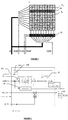
- the selected bits may comprise the Least Significant Bits of the address.
- the scrambler may implement a permutation of the Least Significant Bits (LSB) of the address.
- LLB Least Significant Bits
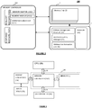
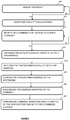
- a row To access memory, a row must first be selected and loaded into the sense amplifiers. This row is then active, and columns may be accessed for read or write.
- a read command may be issued by the memory device controller 102 to initiate a read of a data burst to an active row.
- the row may be charged in the row buffer 15 and read.
- the function F may be an encryption function configured to compute a lightweight encryption on an accessed address and to drop bits resulting from such computation so as to match the expected bitwidth.
- the function F may be based on an encryption algorithm. As encryption algorithms are natively keyed, they respect the constraint of secrecy with respect to an attacker.
- the DDR memory 1 thus maintained scrambled addresses to make it hard for an attacker to hammer a row in its attack process next to the row that is the target of the attack.
Landscapes
- Engineering & Computer Science (AREA)
- Theoretical Computer Science (AREA)
- General Engineering & Computer Science (AREA)
- Computer Security & Cryptography (AREA)
- General Physics & Mathematics (AREA)
- Physics & Mathematics (AREA)
- Computer Hardware Design (AREA)
- Human Computer Interaction (AREA)
- Software Systems (AREA)
- Microelectronics & Electronic Packaging (AREA)
- General Health & Medical Sciences (AREA)
- Virology (AREA)
- Health & Medical Sciences (AREA)
- Storage Device Security (AREA)
- Dram (AREA)
Priority Applications (4)
| Application Number | Priority Date | Filing Date | Title |
|---|---|---|---|
| EP18306854.3A EP3675125A1 (de) | 2018-12-27 | 2018-12-27 | Vorrichtung und verfahren zum schützen eines speichers |
| PCT/EP2019/086849 WO2020136141A1 (en) | 2018-12-27 | 2019-12-20 | Device and method for protecting a memory |
| CN201980090427.6A CN113544779B (zh) | 2018-12-27 | 2019-12-20 | 用于保护存储器的设备和方法 |
| US17/414,910 US12032692B2 (en) | 2018-12-27 | 2019-12-20 | Device and method for protecting a memory |
Applications Claiming Priority (1)
| Application Number | Priority Date | Filing Date | Title |
|---|---|---|---|
| EP18306854.3A EP3675125A1 (de) | 2018-12-27 | 2018-12-27 | Vorrichtung und verfahren zum schützen eines speichers |
Publications (1)
| Publication Number | Publication Date |
|---|---|
| EP3675125A1 true EP3675125A1 (de) | 2020-07-01 |
Family
ID=65903864
Family Applications (1)
| Application Number | Title | Priority Date | Filing Date |
|---|---|---|---|
| EP18306854.3A Pending EP3675125A1 (de) | 2018-12-27 | 2018-12-27 | Vorrichtung und verfahren zum schützen eines speichers |
Country Status (4)
| Country | Link |
|---|---|
| US (1) | US12032692B2 (de) |
| EP (1) | EP3675125A1 (de) |
| CN (1) | CN113544779B (de) |
| WO (1) | WO2020136141A1 (de) |
Cited By (1)
| Publication number | Priority date | Publication date | Assignee | Title |
|---|---|---|---|---|
| FR3137471A1 (fr) * | 2022-07-04 | 2024-01-05 | STMicroelectronics (Grand Ouest) SAS | Procédé de gestion de droits d’accès de régions mémoires et système sur puce correspondant |
Families Citing this family (13)
| Publication number | Priority date | Publication date | Assignee | Title |
|---|---|---|---|---|
| US11556646B2 (en) * | 2019-05-31 | 2023-01-17 | International Business Machines Corporation | Identifying and responding to a side-channel security threat |
| US12027199B2 (en) * | 2021-05-26 | 2024-07-02 | Samsung Electronics Co., Ltd. | Memory device and method of controlling row hammer |
| CN115691603B (zh) * | 2021-07-22 | 2025-10-28 | 长鑫存储技术有限公司 | 锤击地址确定方法及电路、及电子设备 |
| US11688451B2 (en) * | 2021-11-29 | 2023-06-27 | Micron Technology, Inc. | Apparatuses, systems, and methods for main sketch and slim sketch circuit for row address tracking |
| KR102890786B1 (ko) * | 2021-11-30 | 2025-11-26 | 삼성전자주식회사 | 반도체 메모리 장치 및 이를 포함하는 메모리 시스템 |
| US20230205872A1 (en) * | 2021-12-23 | 2023-06-29 | Advanced Micro Devices, Inc. | Method and apparatus to address row hammer attacks at a host processor |
| KR20230099477A (ko) * | 2021-12-27 | 2023-07-04 | 삼성전자주식회사 | 로우 해머 카운터 칩을 포함하는 메모리 모듈들, 이를 포함하는 메모리 시스템 및 메모리 시스템의 동작 방법 |
| US12597459B2 (en) | 2021-12-29 | 2026-04-07 | Micron Technology, Inc. | Apparatuses and methods for row hammer counter mat |
| US20240004801A1 (en) * | 2022-06-29 | 2024-01-04 | Advanced Micro Devices, Inc. | Data encryption suitable for use in systems with processing-in-memory |
| US20240070090A1 (en) * | 2022-08-26 | 2024-02-29 | Apple Inc. | Mitigating Row Hammer Attacks Through Memory Address Encryption |
| US12592271B2 (en) | 2022-12-22 | 2026-03-31 | Micron Technology, Inc. | Apparatuses and methods for increased reliability row hammer counts |
| CN115906087B (zh) * | 2023-03-09 | 2023-07-07 | 长鑫存储技术有限公司 | 行锤攻击保护方法与存储器 |
| CN118520521B (zh) * | 2024-07-22 | 2024-11-05 | 北京开源芯片研究院 | 动态随机存储器的数据行保护方法、装置、设备及存储介质 |
Citations (2)
| Publication number | Priority date | Publication date | Assignee | Title |
|---|---|---|---|---|
| US20150200002A1 (en) * | 2014-01-15 | 2015-07-16 | Jiang Lin | Handling maximum activation count limit and target row refresh in ddr4 sdram |
| US9478263B2 (en) * | 2014-01-17 | 2016-10-25 | Apple Inc. | Systems and methods for monitoring and controlling repetitive accesses to volatile memory |
Family Cites Families (6)
| Publication number | Priority date | Publication date | Assignee | Title |
|---|---|---|---|---|
| US4460958A (en) * | 1981-01-26 | 1984-07-17 | Rca Corporation | Window-scanned memory |
| DE112010005842T8 (de) * | 2010-10-05 | 2014-07-17 | Hewlett-Packard Development Company, L.P. | Verwürfeln einer Adresse und Verschlüsseln von Schreibdaten zum Speichern in einer Speichervorrichtung |
| US9887805B2 (en) * | 2016-06-30 | 2018-02-06 | Tsofun Algorithm Ltd. | Device, system and method for efficient coset decoder by transform |
| US10303398B2 (en) * | 2017-10-26 | 2019-05-28 | Advanced Micro Devices, Inc. | Swizzling in 3D stacked memory |
| KR102091524B1 (ko) * | 2018-07-23 | 2020-03-23 | 삼성전자주식회사 | 어드레스를 스크램블하는 메모리 장치 |
| KR20240045520A (ko) * | 2022-09-30 | 2024-04-08 | 삼성전자주식회사 | 메모리 장치, 그것을 포함하는 메모리 시스템 및 그것의 동작 방법 |
-
2018
- 2018-12-27 EP EP18306854.3A patent/EP3675125A1/de active Pending
-
2019
- 2019-12-20 US US17/414,910 patent/US12032692B2/en active Active
- 2019-12-20 WO PCT/EP2019/086849 patent/WO2020136141A1/en not_active Ceased
- 2019-12-20 CN CN201980090427.6A patent/CN113544779B/zh active Active
Patent Citations (2)
| Publication number | Priority date | Publication date | Assignee | Title |
|---|---|---|---|---|
| US20150200002A1 (en) * | 2014-01-15 | 2015-07-16 | Jiang Lin | Handling maximum activation count limit and target row refresh in ddr4 sdram |
| US9478263B2 (en) * | 2014-01-17 | 2016-10-25 | Apple Inc. | Systems and methods for monitoring and controlling repetitive accesses to volatile memory |
Non-Patent Citations (4)
| Title |
|---|
| ANDREY BOGDANOV; LARS R. KNUDSEN; GREGOR LEANDER; CHRISTOF PAAR; AXEL POSCHMANN; MATTHEW J. B. ROBSHAW; YANNICK SEURIN; CHARLOTTE: "CHES", vol. 4727, 10 September 2007, SPRINGER, article "PRESENT: An Ultra-Lightweight Block Cipher", pages: 450 - 466 |
| MARK SEABORN; THOMAS DULIEN, GOOGLEPROJECTZERO.BLOGSPOT.COM. GOOGLE, RETRIEVED, vol. Exploiti, 9 March 2015 (2015-03-09) |
| SARANI BHATTACHARYA; DEBDEEP MUKHOPADHYAY, CURIOUS CASE OF ROWHAMMER: FLIPPING SECRET EXPONENT BITS USING TIMING ANALYSIS, 4 August 2016 (2016-08-04) |
| YOONGU KIM; ROSS DALY; JEREMIE KIM; CHRIS FALLIN; JI HYE LEE; DONGHYUK LEE; CHRIS WILKERSON; KONRAD LAI; ONUR MUTLU: "Flipping Bits in Memory Without Accessing Them: An experimental Study of DRAM Disturbance Errors", 24 June 2014, IEEE |
Cited By (3)
| Publication number | Priority date | Publication date | Assignee | Title |
|---|---|---|---|---|
| FR3137471A1 (fr) * | 2022-07-04 | 2024-01-05 | STMicroelectronics (Grand Ouest) SAS | Procédé de gestion de droits d’accès de régions mémoires et système sur puce correspondant |
| EP4303736A1 (de) * | 2022-07-04 | 2024-01-10 | STMicroelectronics (Grand Ouest) SAS | Verfahren zur verwaltung von zugriffsrechten für speicherbereiche und entsprechendes system auf einem chip |
| US12547555B2 (en) | 2022-07-04 | 2026-02-10 | STMicroelectronics (Grand Ouest) SAS | Method for managing access rights of memory regions and corresponding system on chip |
Also Published As
| Publication number | Publication date |
|---|---|
| US20220067157A1 (en) | 2022-03-03 |
| CN113544779A (zh) | 2021-10-22 |
| CN113544779B (zh) | 2025-03-25 |
| US12032692B2 (en) | 2024-07-09 |
| WO2020136141A1 (en) | 2020-07-02 |
Similar Documents
| Publication | Publication Date | Title |
|---|---|---|
| US12032692B2 (en) | Device and method for protecting a memory | |
| Wi et al. | Shadow: Preventing row hammer in dram with intra-subarray row shuffling | |
| Bhattacharya et al. | Curious case of rowhammer: flipping secret exponent bits using timing analysis | |
| US8031540B2 (en) | Randomizing current consumption in memory devices | |
| Talukder et al. | PreLatPUF: Exploiting DRAM latency variations for generating robust device signatures | |
| US20180191512A1 (en) | Physically unclonable function generation with direct twin cell activation | |
| US11887686B2 (en) | Fast and efficient system and method for detecting and predicting rowhammer attacks | |
| Vig et al. | Rapid detection of Rowhammer attacks using dynamic skewed hash tree | |
| US12175087B2 (en) | Method and apparatus for protecting memory devices via a synergic approach | |
| US10671546B2 (en) | Cryptographic-based initialization of memory content | |
| Bhattacharya et al. | Advanced fault attacks in software: Exploiting the RowHammer bug | |
| Khan et al. | Cache-out: Leaking cache memory using hardware trojan | |
| Jiang et al. | Trrscope: Understanding target row refresh mechanism for modern ddr protection | |
| EP2990953B1 (de) | Periodische speicherauffrischung in einem sicheren datenverarbeitungssystem | |
| Woo et al. | Rampart: Rowhammer mitigation and repair for server memory systems | |
| Woo et al. | Dapper: A performance-attack-resilient tracker for rowhammer defense | |
| US12499929B2 (en) | Memory controller, memory system including the same, and operating method thereof | |
| US12354640B2 (en) | Memory device refresh operations | |
| KR102925516B1 (ko) | 반도체 장치 및 반도체 장치의 구동 방법 | |
| Lee et al. | Detection Technique of Software-Induced Rowhammer Attacks | |
| US20240169063A1 (en) | Preventing profiled side channel attacks | |
| Awal et al. | Exploring the Correlation Between DRAM Latencies and Rowhammer Attacks | |
| US20230393763A1 (en) | Protection against invalid memory commands | |
| Farmani | Rowhammer Vulnerability Analysis in Dram Memory | |
| KR20220090409A (ko) | 메모리 시스템 및 메모리 시스템의 동작 방법 |
Legal Events
| Date | Code | Title | Description |
|---|---|---|---|
| PUAI | Public reference made under article 153(3) epc to a published international application that has entered the european phase |
Free format text: ORIGINAL CODE: 0009012 |
|
| STAA | Information on the status of an ep patent application or granted ep patent |
Free format text: STATUS: THE APPLICATION HAS BEEN PUBLISHED |
|
| AK | Designated contracting states |
Kind code of ref document: A1 Designated state(s): AL AT BE BG CH CY CZ DE DK EE ES FI FR GB GR HR HU IE IS IT LI LT LU LV MC MK MT NL NO PL PT RO RS SE SI SK SM TR |
|
| AX | Request for extension of the european patent |
Extension state: BA ME |
|
| STAA | Information on the status of an ep patent application or granted ep patent |
Free format text: STATUS: REQUEST FOR EXAMINATION WAS MADE |
|
| 17P | Request for examination filed |
Effective date: 20201222 |
|
| RBV | Designated contracting states (corrected) |
Designated state(s): AL AT BE BG CH CY CZ DE DK EE ES FI FR GB GR HR HU IE IS IT LI LT LU LV MC MK MT NL NO PL PT RO RS SE SI SK SM TR |
|
| STAA | Information on the status of an ep patent application or granted ep patent |
Free format text: STATUS: EXAMINATION IS IN PROGRESS |
|
| 17Q | First examination report despatched |
Effective date: 20250221 |
|
| GRAP | Despatch of communication of intention to grant a patent |
Free format text: ORIGINAL CODE: EPIDOSNIGR1 |
|
| STAA | Information on the status of an ep patent application or granted ep patent |
Free format text: STATUS: GRANT OF PATENT IS INTENDED |
|
| RIC1 | Information provided on ipc code assigned before grant |
Ipc: G11C 7/24 20060101AFI20260316BHEP Ipc: G06F 21/85 20130101ALI20260316BHEP Ipc: G11C 8/20 20060101ALI20260316BHEP Ipc: G11C 11/406 20060101ALI20260316BHEP Ipc: G11C 11/408 20060101ALI20260316BHEP Ipc: G06F 12/14 20060101ALI20260316BHEP |