EP3675128B1 - Schieberegister, ansteuerungsverfahren dafür, ansteuerungsschaltung und anzeigevorrichtung - Google Patents
Schieberegister, ansteuerungsverfahren dafür, ansteuerungsschaltung und anzeigevorrichtung Download PDFInfo
- Publication number
- EP3675128B1 EP3675128B1 EP18829714.7A EP18829714A EP3675128B1 EP 3675128 B1 EP3675128 B1 EP 3675128B1 EP 18829714 A EP18829714 A EP 18829714A EP 3675128 B1 EP3675128 B1 EP 3675128B1
- Authority
- EP
- European Patent Office
- Prior art keywords
- node
- signal
- signal terminal
- control
- circuit
- Prior art date
- Legal status (The legal status is an assumption and is not a legal conclusion. Google has not performed a legal analysis and makes no representation as to the accuracy of the status listed.)
- Active
Links
Images


Classifications
-
- G—PHYSICS
- G09—EDUCATION; CRYPTOGRAPHY; DISPLAY; ADVERTISING; SEALS
- G09G—ARRANGEMENTS OR CIRCUITS FOR CONTROL OF INDICATING DEVICES USING STATIC MEANS TO PRESENT VARIABLE INFORMATION
- G09G3/00—Control arrangements or circuits, of interest only in connection with visual indicators other than cathode-ray tubes
- G09G3/20—Control arrangements or circuits, of interest only in connection with visual indicators other than cathode-ray tubes for presentation of an assembly of a number of characters, e.g. a page, by composing the assembly by combination of individual elements arranged in a matrix no fixed position being assigned to or needed to be assigned to the individual characters or partial characters
- G09G3/22—Control arrangements or circuits, of interest only in connection with visual indicators other than cathode-ray tubes for presentation of an assembly of a number of characters, e.g. a page, by composing the assembly by combination of individual elements arranged in a matrix no fixed position being assigned to or needed to be assigned to the individual characters or partial characters using controlled light sources
- G09G3/30—Control arrangements or circuits, of interest only in connection with visual indicators other than cathode-ray tubes for presentation of an assembly of a number of characters, e.g. a page, by composing the assembly by combination of individual elements arranged in a matrix no fixed position being assigned to or needed to be assigned to the individual characters or partial characters using controlled light sources using electroluminescent panels
- G09G3/32—Control arrangements or circuits, of interest only in connection with visual indicators other than cathode-ray tubes for presentation of an assembly of a number of characters, e.g. a page, by composing the assembly by combination of individual elements arranged in a matrix no fixed position being assigned to or needed to be assigned to the individual characters or partial characters using controlled light sources using electroluminescent panels semiconductive, e.g. using light-emitting diodes [LED]
- G09G3/3208—Control arrangements or circuits, of interest only in connection with visual indicators other than cathode-ray tubes for presentation of an assembly of a number of characters, e.g. a page, by composing the assembly by combination of individual elements arranged in a matrix no fixed position being assigned to or needed to be assigned to the individual characters or partial characters using controlled light sources using electroluminescent panels semiconductive, e.g. using light-emitting diodes [LED] organic, e.g. using organic light-emitting diodes [OLED]
- G09G3/3266—Details of drivers for scan electrodes
-
- G—PHYSICS
- G09—EDUCATION; CRYPTOGRAPHY; DISPLAY; ADVERTISING; SEALS
- G09G—ARRANGEMENTS OR CIRCUITS FOR CONTROL OF INDICATING DEVICES USING STATIC MEANS TO PRESENT VARIABLE INFORMATION
- G09G3/00—Control arrangements or circuits, of interest only in connection with visual indicators other than cathode-ray tubes
- G09G3/20—Control arrangements or circuits, of interest only in connection with visual indicators other than cathode-ray tubes for presentation of an assembly of a number of characters, e.g. a page, by composing the assembly by combination of individual elements arranged in a matrix no fixed position being assigned to or needed to be assigned to the individual characters or partial characters
- G09G3/34—Control arrangements or circuits, of interest only in connection with visual indicators other than cathode-ray tubes for presentation of an assembly of a number of characters, e.g. a page, by composing the assembly by combination of individual elements arranged in a matrix no fixed position being assigned to or needed to be assigned to the individual characters or partial characters by control of light from an independent source
- G09G3/36—Control arrangements or circuits, of interest only in connection with visual indicators other than cathode-ray tubes for presentation of an assembly of a number of characters, e.g. a page, by composing the assembly by combination of individual elements arranged in a matrix no fixed position being assigned to or needed to be assigned to the individual characters or partial characters by control of light from an independent source using liquid crystals
- G09G3/3611—Control of matrices with row and column drivers
- G09G3/3674—Details of drivers for scan electrodes
- G09G3/3677—Details of drivers for scan electrodes suitable for active matrices only
-
- G—PHYSICS
- G11—INFORMATION STORAGE
- G11C—STATIC STORES
- G11C19/00—Digital stores in which the information is moved stepwise, e.g. shift registers
- G11C19/28—Digital stores in which the information is moved stepwise, e.g. shift registers using semiconductor elements
-
- G—PHYSICS
- G09—EDUCATION; CRYPTOGRAPHY; DISPLAY; ADVERTISING; SEALS
- G09G—ARRANGEMENTS OR CIRCUITS FOR CONTROL OF INDICATING DEVICES USING STATIC MEANS TO PRESENT VARIABLE INFORMATION
- G09G2300/00—Aspects of the constitution of display devices
- G09G2300/04—Structural and physical details of display devices
- G09G2300/0421—Structural details of the set of electrodes
- G09G2300/0426—Layout of electrodes and connections
-
- G—PHYSICS
- G09—EDUCATION; CRYPTOGRAPHY; DISPLAY; ADVERTISING; SEALS
- G09G—ARRANGEMENTS OR CIRCUITS FOR CONTROL OF INDICATING DEVICES USING STATIC MEANS TO PRESENT VARIABLE INFORMATION
- G09G2310/00—Command of the display device
- G09G2310/02—Addressing, scanning or driving the display screen or processing steps related thereto
- G09G2310/0264—Details of driving circuits
- G09G2310/0286—Details of a shift registers arranged for use in a driving circuit
-
- G—PHYSICS
- G09—EDUCATION; CRYPTOGRAPHY; DISPLAY; ADVERTISING; SEALS
- G09G—ARRANGEMENTS OR CIRCUITS FOR CONTROL OF INDICATING DEVICES USING STATIC MEANS TO PRESENT VARIABLE INFORMATION
- G09G2310/00—Command of the display device
- G09G2310/08—Details of timing specific for flat panels, other than clock recovery
-
- G—PHYSICS
- G09—EDUCATION; CRYPTOGRAPHY; DISPLAY; ADVERTISING; SEALS
- G09G—ARRANGEMENTS OR CIRCUITS FOR CONTROL OF INDICATING DEVICES USING STATIC MEANS TO PRESENT VARIABLE INFORMATION
- G09G3/00—Control arrangements or circuits, of interest only in connection with visual indicators other than cathode-ray tubes
- G09G3/20—Control arrangements or circuits, of interest only in connection with visual indicators other than cathode-ray tubes for presentation of an assembly of a number of characters, e.g. a page, by composing the assembly by combination of individual elements arranged in a matrix no fixed position being assigned to or needed to be assigned to the individual characters or partial characters
- G09G3/22—Control arrangements or circuits, of interest only in connection with visual indicators other than cathode-ray tubes for presentation of an assembly of a number of characters, e.g. a page, by composing the assembly by combination of individual elements arranged in a matrix no fixed position being assigned to or needed to be assigned to the individual characters or partial characters using controlled light sources
- G09G3/30—Control arrangements or circuits, of interest only in connection with visual indicators other than cathode-ray tubes for presentation of an assembly of a number of characters, e.g. a page, by composing the assembly by combination of individual elements arranged in a matrix no fixed position being assigned to or needed to be assigned to the individual characters or partial characters using controlled light sources using electroluminescent panels
- G09G3/32—Control arrangements or circuits, of interest only in connection with visual indicators other than cathode-ray tubes for presentation of an assembly of a number of characters, e.g. a page, by composing the assembly by combination of individual elements arranged in a matrix no fixed position being assigned to or needed to be assigned to the individual characters or partial characters using controlled light sources using electroluminescent panels semiconductive, e.g. using light-emitting diodes [LED]
- G09G3/3208—Control arrangements or circuits, of interest only in connection with visual indicators other than cathode-ray tubes for presentation of an assembly of a number of characters, e.g. a page, by composing the assembly by combination of individual elements arranged in a matrix no fixed position being assigned to or needed to be assigned to the individual characters or partial characters using controlled light sources using electroluminescent panels semiconductive, e.g. using light-emitting diodes [LED] organic, e.g. using organic light-emitting diodes [OLED]
- G09G3/3225—Control arrangements or circuits, of interest only in connection with visual indicators other than cathode-ray tubes for presentation of an assembly of a number of characters, e.g. a page, by composing the assembly by combination of individual elements arranged in a matrix no fixed position being assigned to or needed to be assigned to the individual characters or partial characters using controlled light sources using electroluminescent panels semiconductive, e.g. using light-emitting diodes [LED] organic, e.g. using organic light-emitting diodes [OLED] using an active matrix
Definitions
- the present disclosure relates to a shift register, a drive method thereof, a drive control circuit, and a display apparatus.
- Gate Drive on Array technologies integrate a drive control circuit of a gate switch of a Thin Film Transistor (TFT) on an array substrate of the display panel to form a control for the gate of the TFT in the display panel, so as to save a Bonding region of the Gate Integrated Circuit (IC) and a wiring space of the Fan-out region, which may not only lower product costs in both aspects of material costs and manufacture processes but also result in symmetry of both sides and a beautiful design of narrow borders for the display panel. Further, such integration processes may further save the Bonding process in a direction of the gate scan line, so as to improve productivity and yield.
- TFT Thin Film Transistor
- the drive control circuit which is the gate drive circuit, consists of a plurality of cascaded shift registers, whereby to sequentially input a gate scan signal to each row of gate lines on the display panel by each stage shift register.
- CN104900268A discloses a shift register, a drive method thereof, a gate drive circuit and a display device.
- signals of a first node and a second node control a first transistor and a second transistor respectively, so that only one of the first transistor and the second transistor is conducted from a first time interval to a fifth time interval, and the suspension of an output is avoided.
- the arrangement of a fifth transistor is equivalent to a diode, so that the effect on the second node by coupling of a fourth capacitor is avoided, the effect on the second node by leakage current flowing to a fifth node is avoided, and the stability of the signal of the output can be guaranteed.
- Embodiments of the invention provide a shift register, comprising: an input sub-circuit, a first control sub-circuit, a second control sub-circuit, a third control sub-circuit, a node stabilization sub-circuit, a first output sub-circuit, and a second output sub-circuit; wherein,
- each of the switch transistors is a P-type transistor
- a first electrode of each of the switch transistors is a source of the P-type transistor
- a second electrode of each of the switch transistors is a drain of the P-type transistor.
- each of the switch transistors is an N-type transistor
- a first electrode of each of the switch transistors is a drain of the N-type transistor
- a second electrode of each of the switch transistors is a source of the N-type transistor.
- embodiments of the invention further provide a drive control circuit, comprising: a plurality of cascaded any one of said shift registers as provided in embodiments of the invention;
- embodiments of the invention further provide a display apparatus, comprising the aforementioned drive control circuit as provided in embodiments of the invention.
- the display apparatus comprises a plurality of light emission control signal lines; a signal output terminal of each stage shift register in the drive control circuit is connected to one of the plurality of light emission control signal lines.
- the drive control circuit is a gate drive circuit.
- embodiments of the invention further provide a drive method of any one of said shift register as provided in embodiments of the invention, comprising: a first stage, a second stage, a third stage, and a fourth stage;
- after the first stage and before the second stage further comprises: at least one insertion stage, wherein the insertion stage comprises a first insertion sub-stage and a second insertion sub-stage;
- a signal of the first clock signal terminal has a same cycle as a signal of the second clock signal terminal, and a percentage of a duration of an active pulse signal of the first clock signal terminal to a duration of one clock cycle is the same as a percentage of a duration of an active pulse signal of the second clock signal terminal to a duration of one said clock cycle; the percentage of a duration of an active pulse signal of the first clock signal terminal to a duration of one said clock cycle is less than or equal to 50%.
- the output of the gate scan signal may be realized by inputting many control signals having different functions, this results in a large number of switch transistors that form each stage shift register in the gate drive circuit and complexity of specific connection structures between the respective switch transistors, which makes the processes harder and increases the production costs. Even, more signal lines are needed to input various control signals having different functions to each stage shift register, which thus results in a decrease in the aperture ratio of the display panel and makes the display panel uncompetitive.
- Embodiments of the invention provide a shift register, a drive method thereof, a drive control circuit, and a display apparatus, for stably outputting signals using a simple structure.
- the shift register comprises: an input sub-circuit, a first control sub-circuit, a second control sub-circuit, a third control sub-circuit, a node stabilization sub-circuit, a first output sub-circuit, and a second output sub-circuit.
- the output signal terminal may be caused to output shifted signals by using a simple structure and less signal lines, which thus simplifies the manufacture processes and lowers the production costs.
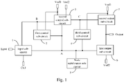
- the shift register comprises: an input sub-circuit 1, a first control sub-circuit 2, a second control sub-circuit 3, a third control sub-circuit 4, a node stabilization sub-circuit 5, a first output sub-circuit 6, and a second output sub-circuit 7;
- the shift register as provided in examples not falling under the present invention comprises: an input sub-circuit 1, a first control sub-circuit 2, a second control sub-circuit 3, a third control sub-circuit 4, a node stabilization sub-circuit 5, a first output sub-circuit 6, and a second output sub-circuit 7;
- the input sub-circuit 1 is used for providing a signal of the input signal terminal to the first node and providing a signal of the first clock signal terminal to the second node, under the control of the first clock signal terminal;
- the first control sub-circuit 2 is used for providing a signal of the first reference signal terminal to the second node under the control of the first node;
- the second control sub-circuit 3 is used for providing a signal of the first reference signal terminal to the third node under the control of a signal of the first node, and providing a signal of the second reference signal terminal to the third node under the control of a signal of the second node;
- the third control sub-circuit 4 is used for providing
- the shift register as provided in examples not falling under the present invention may cause the output signal terminal to stably output shifted signals by using a simple structure and less signal lines, which thus simplifies the manufacture processes and lowers the production costs.
- the active pulse signal of the input signal terminal is a high potential signal
- the signal of the first reference signal terminal is a high potential signal
- the signal of the second reference signal terminal is a low potential signal
- the active pulse signal of the input signal terminal is a low potential signal
- the signal of the first reference signal terminal is a low potential signal
- the signal of the second reference signal terminal is a high potential signal.
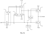
- the input sub-circuit 1 comprises a first switch transistor M1 and a second switch transistor M2;
- the first switch transistor M1 and the second switch transistor M2 may be P-type transistors.
- the first switch transistor M1 and the second switch transistor M2 may be N-type transistors. No limit is made herein.
- the first switch transistor when the first switch transistor is in a conductive state under the control of a signal of the first clock signal terminal, it provides a signal of the input signal terminal to the first node.
- the second switch transistor when the second switch transistor is in a conductive state under the control of a signal of the first clock signal terminal, it provides a signal of the first clock signal terminal to the second node.
- the first control sub-circuit 2 comprises a third switch transistor M3; a control electrode of the third switch transistor M3 is connected to the first node A, a first electrode of the third switch transistor M3 is connected to the first reference signal terminal Vref1, and a second electrode of the third switch transistor M3 is connected to the second node B.
- the third switch transistor M3 may be a P-type transistor.
- the third switch transistor M3 may be an N-type transistor. No limit is made therein.
- the third switch transistor when the third switch transistor is in a conductive state under the control of a signal of the first node, it provides a signal of the first reference signal terminal to the second node.
- the second control sub-circuit 3 comprises a fourth switch transistor M4 and a fifth switch transistor M5;
- the fourth switch transistor M4 and the fifth switch transistor M5 may be P-type transistors.
- the fourth switch transistor M4 and the fifth switch transistor M5 may be N-type transistors. No limit is made herein.
- the fourth switch transistor when the fourth switch transistor is in a conductive state under the control of a signal of the first node, it provides a signal of the first reference signal terminal to the third node.
- the fifth switch transistor when the fifth switch transistor is in a conductive state under the control of the second node, it provides a signal of the second reference signal terminal to the third node.
- the third control sub-circuit 4 comprises a sixth switch transistor M6; a control electrode of the sixth switch transistor M6 is connected to the third node C, a first electrode of the sixth switch transistor M6 is connected to the first reference signal terminal Vref1, and a second electrode of the sixth switch transistor M6 is connected to the first node A.
- the sixth switch transistor M6 may be a P-type transistor.
- the sixth switch transistor M6 may be an N-type transistor. No limit is made herein.
- the sixth switch transistor when the sixth switch transistor is in a conductive state under the control of a signal of the third node, it provides a signal of the first reference signal terminal to the first node.
- the first output sub-circuit 6 comprises a seventh switch transistor M7; a control electrode of the seventh switch transistor M7 is connected to the first node A, a first electrode of the seventh switch transistor M7 is connected to the second reference signal terminal Vref2, and a second electrode of the seventh switch transistor M7 is connected to the output signal terminal "Output" (the output terminal).
- the seventh switch transistor M7 may be a P-type transistor.
- the seventh switch transistor M7 may be an N-type transistor. No limit is made herein.
- the seventh switch transistor when the seventh switch transistor is in a conductive state under the control of a signal of the first node, it provides a signal of the second reference signal terminal to the output signal terminal.
- the second output sub-circuit 7 comprises an eight switch transistor M8; a control electrode of the eight switch transistor M8 is connected to the third node C, a first electrode of the eight switch transistor M8 is connected to the first reference signal terminal Vref1, and a second electrode of the eight switch transistor M8 is connected to the output signal terminal "Output" (the output terminal).
- the eight switch transistor M8 may be a P-type transistor.
- the eight switch transistor M8 may be an N-type transistor. No limit is made herein.
- the eight switch transistor when the eight switch transistor is in a conductive state under the control of a signal of the third node, it provides a signal of the first reference signal terminal to the output signal terminal.
- the node stabilization sub-circuit 5 comprises capacitor Cst.
- a first terminal of the capacitor Cst is connected to the first node A, and a second terminal of the capacitor Cst is connected to the second clock signal terminal CK2.
- the capacitor maintains a stable potential of the signal of the first node. Moreover, when the first node is in a floating state, a coupling effect of the capacitor maintains a stable voltage difference of both terminals of the capacitor, that is, maintain a stable voltage difference between the first node and the second clock signal terminal.
- Exemplary structures of the respective sub-circuits in the shift register as provided in embodiments of the invention are only illustrated above, and during an exemplary implementation, structures of the aforementioned respective sub-circuits are not limited to the aforementioned structures as provided in embodiments of the invention, and may be other structures known by those skilled in the art. No limit is made herein.
- each of the switch transistors may be a P-type transistor.
- each of the switch transistors may be an N-type transistor.
- the P-type transistor is turned off under the action of a high potential signal and is conductive under the action of a low potential signal
- the N-type transistor is conductive under the action of a high potential signal and is turned off under the action of a low potential signal
- the switch transistors as mentioned in the aforementioned embodiments of the invention may be either Thin Film Transistors (TFTs) or Metal Oxide Semiconductor (MOS) field effect transistors. No limit is made herein.
- a control electrode of each of said switch transistors is used as a gate thereof, and based on a signal of the gate and a type of the signal of each of said switch transistors, a first electrode may be used as a source and a second electrode may be used as a drain. Alternatively, a first electrode may be used as a drain and a second electrode may be used as a source. No limit is made herein.
- a signal of the first clock signal terminal has a same cycle as a signal of the second clock signal terminal, and a percentage of a duration of an active pulse signal of the first clock signal terminal to a duration of one clock cycle is the same as a percentage of a duration of an active pulse signal of the second clock signal terminal to a duration of one said clock cycle.
- the active pulse signal of the first clock signal terminal is used for controlling conduction of the first transistor and the fifth transistor.
- a percentage of a duration of an active pulse signal of the first clock signal terminal to a duration of one clock cycle may be equal to 50%.
- a percentage of a duration of an active pulse signal of the first clock signal terminal to a duration of one clock cycle may be less than 50%, during an exemplary implementation.
- both the percentage of a duration of an active pulse signal of the first clock signal terminal CK1 to a duration of one clock cycle and the percentage of a duration of an active pulse signal of the second clock signal terminal CK2 to a duration of one clock cycle are less than 50%.
- an active pulse signal of the input signal terminal "Input" (the input terminal) is a high potential signal, and both an active pulse signal of the first clock signal terminal CK1 and an active pulse signal of the second clock signal terminal CK2 are low potential signals.
- an active pulse signal of the input signal terminal may be a low potential signal.
- both an active pulse signal of the first clock signal terminal and an active pulse signal of the second clock signal terminal are high potential signals.
- the aforementioned percentages can be designed and determined according to actual application environments. No limit is made herein.
- a structure of the shift register as shown in FIG. 2a is taken as an example to describe the operation process thereof.
- a signal of the first reference signal terminal Vref1 is a high potential signal
- a signal of the second reference signal terminal Vref2 is a low potential signal.
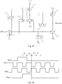
- a corresponding input/output timing diagram is as shown in FIG. 3a , for example, four stages T1, T2, T3 and T4 in the input/output timing diagram as shown in FIG. 3a are selected.
- both the first switch transistor M1 and the second switch transistor M2 are conductive.
- the conductive first switch transistor M1 provides a high potential signal of the input signal terminal "Input" to the first node A such that a signal of the first node A is a high potential signal, and thus all the third switch transistor M3, the fourth switch transistor M4, and the seventh switch transistor M7 are turned off.
- the conductive second switch transistor M2 provides a low potential signal of the first clock signal terminal CK1 to the second node B such that a signal of the second node B is a low potential signal
- the fifth switch transistor M5 is conductive to provide a low potential signal of the second reference signal terminal Vref2 to the third node C such that a signal of the third node C is a low potential signal
- both the sixth switch transistor M6 and the eighth switch transistor M8 are conductive.
- the conductive sixth switch transistor M6 provides a high potential signal of the first reference signal terminal Vref1 to the first node A such that a signal of the first node A is a high potential signal.
- the conductive eighth switch transistor M8 provides a high potential signal of the first reference signal terminal Vref1 to the output signal terminal "Output" (the output terminal), such that the output signal terminal "Output" (the output terminal) outputs a high potential signal.
- both the first switch transistor M1 and the second switch transistor M2 are turned off. Since no additional signal is input to the second node B to charge the second node B, the second node B maintains a low potential signal, such that the fifth switch transistor M5 is conductive to provide the low potential signal of the second reference signal terminal Vref2 to the third node C and that a signal of the third node C is a low potential signal, and thus both the sixth switch transistor M6 and the eight switch transistor M8 are conductive.
- the conductive sixth switch transistor M6 provides a high potential signal of the first reference signal terminal Vref1 to the first node A such that a signal of the first node A is a high potential signal, and thus all the third switch transistor M3, the fourth switch transistor M4, and the seventh switch transistor M7 are turned off.
- the conductive eighth switch transistor M8 provides a high potential signal of the first reference signal terminal Vref1 to the output signal terminal "Output" (the output terminal) such that the output signal terminal "Output" (the output terminal) outputs a high potential signal.
- a simultaneous inversion may be avoided between a potential of a signal of the first clock signal terminal CK1 having a percentage of 50% and a potential of a signal of the second clock signal terminal CK2, which results in a loss of the shift register which is caused by conduction and short circuit of the second reference signal terminal Vref2 connected to the seventh transistor M7 and the first reference signal terminal Vref1 connected to the eighth transistor M8, and thus makes the output of the circuit more stable.
- both the first switch transistor M1 and the second switch transistor M2 are conductive.
- the conductive first switch transistor M1 provides a low potential signal of the input signal terminal "Input" (the input terminal) to the first node A such that a signal of the first node A is a low potential signal, and thus all the third switch transistor M3, the fourth switch transistor M4, and the seventh switch transistor M7 are conductive and the capacitor Cst is charged.
- the conductive third switch transistor M3 provides a high potential signal of the first reference signal terminal Vref1 to the second node B such that a signal of the second node B is a high potential signal, and thus the fifth switch transistor M5 is turned off.
- the conductive fourth switch transistor M4 provides a high potential signal of the first reference signal Vref1 to the third node C such that a signal of the third signal C is a high potential signal, and thus both sixth switch transistor M6 and the eighth switch transistor M8 are turned off.
- the conductive seventh switch transistor M7 provides a low potential signal of the second reference signal terminal Vref2 to the output signal terminal "Output" (the output terminal) such that the output signal terminal "Output" (the output terminal) outputs a low potential signal.
- the completely conductive third switch transistor M3 provides a high potential signal of the first reference signal terminal Vref to the second node B without any voltage loss such that a signal of the second node B is a high potential signal, and thus the fifth switch transistor M5 can be completely turned off.
- the completely conductive fourth switch transistor M4 provides a high potential signal of the first reference signal terminal Vref1 to the third node C without any voltage loss such that a signal of the third node C is a high potential signal, and thus both the sixth switch transistor M6 and the eighth switch transistor M8 are completely turned off.
- the completely conductive seventh switch transistor M7 provides a low potential signal of the second reference signal terminal Vref2 to the output signal terminal "Output" (the output terminal) without any voltage loss such that the output signal terminal "Output" (the output terminal) completely outputs a low potential signal.
- the aforementioned shift register as provided in embodiments of the invention repeats the operation processes of stage T3 and stage T4 after stage T4, until a next frame starts.
- the aforementioned shift register as provided in embodiments of the invention may realize a stable shift output of the signal only by using a simple structure of eight switch transistors and one capacitor.
- VGL respectively represents a voltage of a low potential signal of the input signal terminal "Input" (the input terminal), a voltage of a low potential signal of the second reference signal terminal Vref2, and a voltage of a low potential signal of the second clock signal terminal CK2
- VGH represents a voltage of a high potential signal of the second clock signal terminal CK2
- a threshold voltage of each of the switch transistors is set as V th .
- both a gate of the first switch transistor M1 and the signal to be transmitted are a low potential signal, such that the signal transmitted to the first node A has a voltage of VGL-V th . Due to the same reason, both a gate of the seventh switch transistor and the signal to be transmitted are also a low potential signal, which thus causes a signal output from the signal output terminal "Output" (the output terminal) to have a voltage of VGL-2V th such that a voltage of a low potential signal output from the signal output terminal "Output" (the output terminal) cannot reach VGL.
- stage T4 since the second clock signal terminal CK2 changes from a high potential signal to a low potential signal, a potential of a signal of the first node A is further pulled down due to a coupling effect of the capacitor Cst, such that the voltage of the signal of the first node A jumps to VGL-V th -(VGH+
- a structure of the shift register as shown in FIG. 2a is taken as an example to describe the exemplary operation process thereof.
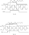
- An insertion stage T01 is inserted between stage T1 and stage T2 in the timing diagram of the aforementioned embodiment as shown in FIG. 3a , that is to say, on the basis of the aforementioned embodiment as shown in FIG. 3a , a duration of an active pulse signal of the input signal terminal "Input" (the input terminal) is extended by one clock cycle, and a corresponding input/output timing diagram is as shown in FIG. 3b .
- five stages of T1, T01, T2, T3, and T4 are selected, wherein the insertion stage T01 is further divided into a first insertion sub-stage T011 and a second insertion sub-stage T012.
- the specific operation process during this stage is substantially the same as the operation process during stage T1 in the aforementioned embodiment as shown in FIG.3a . No detailed description is given herein.
- both the first switch transistor M1 and the second switch transistor M2 are turned off. Since no additional signal is input to the second node B to charge the second node B, the second node B maintains a low potential signal such that the fifth switch transistor M5 is conductive to provide a low potential signal of the second reference signal terminal Vref2 to the third node C and that a signal of the third node C is a low potential signal, and thus both the sixth switch transistor M6 and the eighth switch transistor M8 are conductive.
- the conductive sixth switch transistor M6 provides a high potential signal of the first reference signal terminal Vref1 to the first node A such that a signal of the first node A is a high potential signal, and thus all the third switch transistor M3, the fourth switch transistor M4, and the seventh switch transistor M7 are turned off.
- the conductive eighth switch transistor M8 provides a high potential signal of the first reference signal terminal Vref1 to the output signal terminal "Output" (the output terminal) such that the output signal terminal "Output" (the output terminal) outputs a high potential signal.
- both the first switch transistor M1 and the second switch transistor M2 are conductive.
- the conductive first switch transistor M1 provides a high potential signal of the input signal terminal "Input" to the first node A such that a signal of the first node A is a high potential signal, and thus all the third switch transistor M3, the fourth switch transistor M4, and the seventh switch transistor M7 are turned off.
- the conductive second switch transistor M2 provides a low potential signal of the first clock signal terminal CK1 to the second node B such that a signal of the second node B is a low potential signal
- the fifth switch transistor M5 is conductive to provide a low potential signal of the second reference signal terminal Vref2 to the third node C such that a signal of the third node C is a low potential signal
- both the sixth switch transistor M6 and the eighth switch transistor M8 are conductive.
- the conductive sixth switch transistor M6 provides a high potential signal of the first reference signal terminal Vref1 to the first node A such that a signal of the first node A is a high potential signal.
- the conductive eighth switch transistor M8 provides the high potential signal of the first reference signal Vref1 to the output signal terminal "Output" (the output terminal) such that the output signal terminal "Output" (the output terminal) outputs a high potential signal.
- the operation process during this stage is substantially the same as the operation process during stage T2 in the aforementioned embodiment as shown in FIG.3a . No detailed description is given herein.
- the operation process during this stage is substantially the same as the operation process during stage T3 in the aforementioned embodiment as shown in FIG.3a . No detailed description is given herein.
- the operation process during this stage is substantially the same as the operation process during stage T4 in the aforementioned embodiment as shown in FIG.3a . No detailed description is given herein.
- the aforementioned shift register as provided in embodiments of the invention repeats the operation processes of stage T3 and stage T4 after stage T4, until a next frame starts.
- the aforementioned shift register as provided in embodiments of the invention may realize a stable shift output of the signal only by using a simple structure of eight switch transistors and one capacitor.
- FIG. 2a The structure as shown in FIG. 2a is taken as an example, and the operation process of the shift register is simulated by using the simulation timing diagrams of respective input signals as shown in FIGS. 4a and 4b .
- the vertical ordinate represents a voltage and the horizontal ordinate represents a time
- L1 in FIG. 4a represents a signal of the input signal terminal "Input" (the input terminal)
- L2 represents a signal of the first clock signal terminal CK1
- L3 represents a signal of the second clock signal terminal CK2.
- a signal of the output signal terminal "Output" changes as shown in FIG. 4c .
- FIG. 4c In FIG.
- the vertical ordinate represents a voltage and the horizontal ordinate represents a time. From FIG. 4c , it can be further seen that, the aforementioned shift register as provided in embodiments of the invention runs stably, such that the signal output terminal "Output" (the output terminal) stably outputs a signal L4.
- T1 six stages of T1, T01, T02, T2, T3, and T4 are selected, wherein the insertion stage T01 is further divided into a first insertion sub-stage T011 and a second insertion sub-stage T012; the insertion stage T02 is further divided into a first insertion sub-stage T021 and a second insertion sub-stage T022.
- the specific operation process during this stage is substantially the same as the operation process during stage T1 in the aforementioned embodiment as shown in FIG.3a . No detailed description is given herein.
- both the first switch transistor M1 and the second switch transistor M2 are turned off. Since no additional signal is input to the second node B to charge the second node B, the second node B maintains a low potential signal such that the fifth switch transistor M5 is conductive to provide a low potential signal of the second reference signal terminal Vref2 to the third node C and that a signal of the third node C is a low potential signal, and thus both the sixth switch transistor M6 and the eighth switch transistor M8 are conductive.
- the conductive sixth switch transistor M6 provides a high potential signal of the first reference signal terminal Vref1 to the first node A such that a signal of the first node A is a high potential signal, and thus all the third switch transistor M3, the fourth switch transistor M4, and the seventh switch transistor M7 are turned off.
- the conductive eighth switch transistor M8 provides a high potential signal of the first reference signal terminal Vref1 to the output signal terminal "Output" (the output terminal) such that the output signal terminal "Output" (the output terminal) outputs a high potential signal.
- both the first switch transistor M1 and the second switch transistor M2 are conductive.
- the conductive first switch transistor M1 provides a high potential signal of the input signal terminal "Input" (the input terminal) to the first node A such that a signal of the first node A is a high potential signal, and thus all the third switch transistor M3, the fourth switch transistor M4, and the seventh switch transistor M7 are turned off.
- the conductive second switch transistor M2 provides a low potential signal of the first clock signal terminal CK1 to the second node B such that a signal of the second node B is a low potential signal
- the fifth switch transistor M5 is conductive to provide a low potential signal of the second reference signal terminal Vref2 to the third node C such that a signal of the third node C is a low potential signal
- both the sixth switch transistor M6 and the eighth switch transistor M8 are conductive.
- the conductive sixth switch transistor M6 provides a high potential signal of the first reference signal terminal Vref1 to the first node A such that a signal of the first node A is a high potential signal.
- the conductive eighth switch transistor M8 provides the high potential signal of the first reference signal Vref1 to the output signal terminal "Output" (the output terminal) such that the output signal terminal "Output" (the output terminal) outputs a high potential signal.
- both the first switch transistor M1 and the second switch transistor M2 are turned off. Since no additional signal is input to the second node B to charge the second node B, the second node B maintains a low potential signal, such that the fifth switch transistor M5 is conductive to provide the low potential signal of the second reference signal terminal Vref2 to the third node C and that a signal of the third node C is a low potential signal, and thus both the sixth switch transistor M6 and the eight switch transistor M8 are conductive.
- the conductive sixth switch transistor M6 provides a high potential signal of the first reference signal terminal Vref1 to the first node A such that a signal of the first node A is a high potential signal, and thus all the third switch transistor M3, the fourth switch transistor M4, and the seventh switch transistor M7 are turned off.
- the conductive eighth switch transistor M8 provides a high potential signal of the first reference signal terminal Vref1 to the output signal terminal "Output" (the output terminal) such that the output signal terminal "Output" (the output terminal) outputs a high potential signal.
- both the first switch transistor M1 and the second switch transistor M2 are conductive.
- the conductive first switch transistor M1 provides a high potential signal of the input signal terminal "Input" (the input terminal) to the first node A such that a signal of the first node A is a high potential signal, and thus all the third switch transistor M3, the fourth switch transistor M4, and the seventh switch transistor M7 are turned off.
- the conductive second switch transistor M2 provides a low potential signal of the first clock signal terminal CK1 to the second node B such that a signal of the second node B is a low potential signal
- the fifth switch transistor M5 is conductive to provide a low potential signal of the second reference signal terminal Vref2 to the third node C such that a signal of the third node C is a low potential signal
- both the sixth switch transistor M6 and the eighth switch transistor M8 are conductive.
- the conductive sixth switch transistor M6 provides a high potential signal of the first reference signal terminal Vref1 to the first node A such that a signal of the first node A is a high potential signal.
- the conductive eighth switch transistor M8 provides a high potential signal of the first reference signal terminal Vref1 to the output signal terminal "Output" (the output terminal) such that the output signal terminal "Output" (the output terminal) outputs a high potential signal.
- the operation process during this stage is substantially the same as the operation process during stage T2 in the aforementioned embodiment as shown in FIG.3a . No detailed description is given herein.
- the operation process during this stage is substantially the same as the operation process during stage T3 in the aforementioned embodiment as shown in FIG.3a . No detailed description is given herein.
- the operation process during this stage is substantially the same as the operation process during stage T4 in the aforementioned embodiment as shown in FIG.3a . No detailed description is given herein.
- the aforementioned shift register as provided in embodiments of the invention repeats the operation processes of stage T3 and stage T4 after stage T4, until a next frame starts.
- the aforementioned shift register as provided in embodiments of the invention may realize a stable shift output of the signal only by using a simple structure of eight switch transistors and one capacitor.
- the aforementioned shift register as provided in embodiments of the invention extends the duration of the active pulse signal of the input signal terminal by one clock signal cycle such that the output signal terminal can output a signal of a corresponding duration in the aforementioned embodiment as shown in FIG. 3b , extends the duration of the active pulse signal of the input signal terminal by two clock signal cycles such that the output signal terminal can output a signal of a corresponding duration in the aforementioned embodiment as shown in FIG. 3c , and so on.
- the output signal terminal may be caused to output a signal having a duration that is the same as the duration of the active pulse signal of the input signal terminal.
- the aforementioned shift register can control the duration of the active pulse signal of the signal output from the signal output terminal only by changing the duration of the active pulse signal of the input signal terminal, without the necessity of alterations of circuits and changes of processes, which thus may reduce process complexity and may lower costs.
- a signal of the first reference signal terminal Vref1 is a low potential signal
- a signal of the second reference signal terminal Vref2 is a high potential signal
- a signal of the input signal terminal "Input" (the input terminal)
- a signal of the first clock signal terminal CK1 and a signal of the second clock signal terminal CK2 in the input/output timing diagram corresponding thereto have potentials opposite to those of the corresponding signals in FIGS. 3a , 3b, and 3c . That is to say, a high potential of the respective signals in FIGS.
- the operation process may refer to the operation process in the aforementioned respective embodiment, which merely changes a high potential signal to a low potential and changes a low potential signal to a high potential signal for the control electrode of each of the switch transistors in each of the aforementioned embodiments. No detailed description is given herein.
- embodiments of the invention further provide a drive method of any one of said shift register as provided in embodiments of the invention, as shown in FIG. 5 , the drive method comprises: a first stage, a second stage, a third stage, and a fourth stage;
- the input sub-circuit provides a signal of the input signal terminal to the first node and provides a signal of the first clock signal terminal to the second node, under the control of the first clock signal terminal;
- the second control sub-circuit provides a signal of the second reference signal terminal to the third node under the control of the second node;
- the third control sub-circuit provides a signal of the first reference signal terminal to the first node under the control of the third node;
- the second output sub-circuit provides the signal of the first reference signal terminal to the output signal terminal under the control of a signal of the third node;
- the second control sub-circuit provides a signal of the second reference signal terminal to the third node under the control of the second node;
- the third control sub-circuit provides a signal of the first reference signal terminal to the first node under the control of the third node;
- the second output sub-circuit provides a signal of the first reference signal to the output signal terminal under the control of the signal of the third node;
- the input sub-circuit provides a signal of the input signal terminal to the first node and provides a signal of the first clock signal to the second node, under the control of the first control signal terminal;
- the first control sub-circuit provides a signal of the first reference signal terminal to the second node under the control of the first node;
- the second control sub-circuit provides a signal of the first reference signal terminal to the third node under the control of a signal of the first node;
- the first output sub-circuit provides a signal of the second reference signal terminal to the output signal terminal under the control of a signal of the first node;
- the node stabilization sub-circuit stabilizes a potential of the first node; the first control sub-circuit provides a signal of the first reference signal terminal to the second node under the control of the first node; the second control sub-circuit provides the signal of the first reference signal terminal to the third node under the control of a signal of the first node; the first output sub-circuit provides a signal of the second reference signal terminal to the output signal terminal under the control of the signal of the first node.
- the drive method of the aforementioned shift register as provided in embodiments of the invention may stably output shifted signals, which simplifies the manufacture processes and lowers the production costs.
- the drive method as provided in embodiments of the invention may further comprise: at least one insertion stage, wherein the insertion stage comprises a first insertion sub-stage and a second insertion sub-stage;
- the aforementioned drive method as provided in embodiments of the invention can control a duration of an active pulse signal of the signal output from the signal output terminal only by inserting at least one insertion stage, without the necessity of alterations of circuits and changes of processes, which thus may simplify the manufacture processes, lower the production costs, and facilitate the realization of design of narrow borders of the panel in the display apparatus.
- one insertion stage is inserted between the first stage and the second stage, which operation process corresponds the aforementioned embodiment as shown in FIG. 3b .
- Two insertion stages are inserted between the first stage and the second stage, which operation process corresponds the embodiment as shown in FIG. 3c .
- three, four, or more insertion stages may be inserted between the first stage and the second stage. No detailed description is given herein.
- a signal of the first clock signal terminal has a same cycle as a signal of the second clock signal terminal, and a percentage of a duration of an active pulse signal of the first clock signal terminal to a duration of one clock cycle is the same as a percentage of a duration of an active pulse signal of the second clock signal terminal to a duration of one clock cycle, wherein, the active pulse signal of the first clock signal terminal is used for controlling conduction of the first transistor and the fifth transistor.
- a percentage of a duration of an active pulse signal of the first clock signal terminal to a duration of one clock cycle may be equal to 50%.
- a percentage of a duration of an active pulse signal of the first clock signal terminal to a duration of one clock cycle may be less than 50%, during a specific implementation.
- both the percentage of a duration of an active pulse signal of the first clock signal terminal CK1 to a duration of one clock cycle and the percentage of a duration of an active pulse signal of the second clock signal terminal CK2 to a duration of one clock cycle are less than 50%.
- an active pulse signal of the input signal terminal "Input" (the input terminal) is a high potential signal, and both an active pulse signal of the first clock signal terminal CK1 and an active pulse signal of the second clock signal terminal CK2 are low potential signals.
- an active pulse signal of the input signal terminal may also be a low potential signal.
- both an active pulse signal of the first clock signal terminal and an active pulse signal of the second clock signal terminal are high potential signals.
- the aforementioned percentages can be designed and determined according to actual application environments. No limit is made herein.
- embodiments of the invention further provide a drive control circuit, as shown in FIG. 6 , the drive control circuit comprises: a plurality of any one of said cascaded shift registers as provided in embodiments of the invention: SR(1), SR(2) ⁇ SR(N) ⁇ SR(N-1), SR(N) (totally N shift registers, 1 ⁇ n ⁇ N); N is a positive integer, and n is a positive integer;
- each of the shift registers in the aforementioned drive control circuit is the same as the aforementioned shift register of the invention in terms of function and structure. No detailed description is given herein.
- the aforementioned drive control circuit as provided in embodiments of the invention may be used for providing a light emission control signal of the light emission control transistor, or may be used for providing a gate scan signal of the scan control transistor. No limit is made herein.
- both the first clock signal terminal CK1 of the (2k-1)th-stage shift register and the second clock signal terminal CK2 of the 2kth-stage shift register are connected to the same clock terminal, namely the first clock signal CK1; both the second clock signal terminal CK2 of the (2k-1)th-stage shift register and the first clock signal terminal CK1 of the 2kth-stage shift register are connected to the same clock terminal, namely the second clock signal CK2, wherein k is a positive integer.
- the first reference signal terminal Vref1 of each stage shift register SR(n) is connected to the same signal terminal, namely the first reference terminal Vref1; the second reference signal terminal Vref2 of each stage shift register SR(n) is connected to the same signal terminal, namely the second reference terminal Vref1.
- embodiments of the invention further provide a display apparatus, the display apparatus comprises the aforementioned drive control circuit as provided in embodiments of the invention.
- the implementation of the display apparatus may refer to embodiments of the aforementioned shift register. No detailed description is given herein.
- the aforementioned display apparatus as provided in embodiments of the invention may be an organic light-emitting display apparatus or a liquid crystal display apparatus. No limit is made herein.
- the organic light-emitting display apparatus is generally provided with a plurality of organic light-emitting diodes, a pixel compensation circuit which is connected to each of the plurality of organic light-emitting diodes, a plurality of gate lines, and a plurality of light emission control signal lines.
- the pixel compensation circuit is generally provided with a light emission control transistor for controlling light emission of the organic light-emitting diodes and a scan control transistor for controlling input of data signals.
- a control electrode of the light emission control transistor is connected to a light emission control signal line corresponding to a row where it resides, for receiving a light emission control signal; a control electrode of the scan control transistor is connected to a gate line corresponding to a row where it resides, for receiving a gate scan signal.
- the drive control circuit may be used for providing a light emission control signal of the light emission control transistor, wherein a signal output terminal of each stage shift register in the drive control circuit is connected to one of the light emission control signal lines.
- the drive control circuit may be also used for providing a gate scan signal of the scan control transistor, wherein the drive control circuit is a gate drive circuit, and a signal output terminal of each stage shift register in the drive control circuit is connected to one of the gate lines.
- two drive control circuits may be provided, wherein one drive control circuit is used for providing a light emission control signal of the light emission control transistor, and a signal output terminal of each stage shift register in the drive control circuit is connected to one of the light emission control signal lines; the other drive control circuit is used as a gate drive circuit for providing a gate scan signal of the scan control transistor, and a signal output terminal of each stage shift register in the drive control circuit is connected to one of the gate lines. No limit is made herein.
- the aforementioned display apparatus as provided in embodiments of the invention is a liquid crystal display apparatus
- a plurality of pixel electrodes, a switch transistor which is connected to each of the plurality of pixel electrodes, and a plurality of gates are generally provided.
- control electrodes of each row of switch transistors are connected to a gate line corresponding to the row where they reside.
- the aforementioned drive control circuit as provided in embodiments of the invention may be used as a gate drive circuit for providing a gate drive signal of the switch transistor, and a signal output terminal of each stage shift register in the drive control circuit is connected to one of the gate lines.
- the display apparatus as provided in embodiments of the invention may be a mobile phone, a tablet computer, a TV set, a display, a laptop, a digital photo frame, a navigator, or any other product or component having a display function.
- Other indispensable component parts of the display apparatus are owned as understood by those skilled in the art, which is not further described herein and should not be used as a limit to the present disclosure.
- the shift register comprises: an input sub-circuit, a first control sub-circuit, a second control sub-circuit, a third control sub-circuit, a node stabilization sub-circuit, a first output sub-circuit, and a second output sub-circuit.
- the input sub-circuit is used for providing a signal of the input signal terminal to the first node and providing a signal of the first clock signal terminal to the second node, under the control of the first clock signal terminal;
- the first control sub-circuit is used for providing a signal of the first reference signal terminal to the second node under the control of the first node;
- the second control sub-circuit is used for providing a signal of the first reference signal terminal to the third node under the control of a signal of the first node, and for providing a signal of the second reference signal terminal to the third node under the control of the third node;
- the third control sub-circuit is used for providing signal of the first reference signal terminal to the first node under the control of the third node;
- the node stabilization sub-circuit is used for stabilizing a potential of the first node;
- the first output sub-circuit is used for providing a signal of the second reference signal terminal to the output signal terminal under the control of a signal of the first node;
- the shift register as provided in embodiments of the invention causes the output signal terminal to stably output shifted signals by using a simple structure and less signal lines, which thus simplifies the manufacture processes and lowers the production costs.
- the aforementioned seven sub-circuits it is possible to control the duration of the active pulse signal of the signal output from the signal output terminal only by changing the duration of the active pulse signal of the input signal terminal, without the necessity of alterations of circuits and changes of processes, which thus may simplify the manufacture processes, lower the production costs, and facilitate the realization of design of narrow borders of the panel in the display apparatus.
Landscapes
- Engineering & Computer Science (AREA)
- Physics & Mathematics (AREA)
- Computer Hardware Design (AREA)
- General Physics & Mathematics (AREA)
- Theoretical Computer Science (AREA)
- Chemical & Material Sciences (AREA)
- Crystallography & Structural Chemistry (AREA)
- Liquid Crystal Display Device Control (AREA)
- Control Of Indicators Other Than Cathode Ray Tubes (AREA)
- Shift Register Type Memory (AREA)
Claims (8)
- Schieberegister, umfassend: Eine Eingangsteilschaltung (1), eine erste Steuerteilschaltung (2), eine zweite Steuerteilschaltung (3), eine dritte Steuerteilschaltung (4), eine Knotenstabilisierungsteilschaltung (5), eine erste Ausgangsteilschaltung (6) und eine zweite Ausgangsteilschaltung (7); wobei,die Eingangsteilschaltung (1), die jeweils mit einem Eingangssignalanschluss, einem ersten Taktsignalanschluss (CK1), einem ersten Knoten (A) und einem zweiten Knoten (B) verbunden ist, zum Bereitstellen eines Signals des Eingangssignalanschlusses an den ersten Knoten (A) dient und zum Bereitstellen eines Signals des ersten Taktsignalanschlusses (CK1) an den zweiten Knoten (B), mittels einer Steuerung des ersten Taktsignalanschlusses (CK1);die erste Steuerteilschaltung (2), die jeweils mit einem ersten Referenzsignalanschluss (Vref1), dem ersten Knoten (A) und dem zweiten Knoten (B) verbunden ist, zum Bereitstellen eines Signals des ersten Referenzsignalanschlusses (Vref1) an den zweiten Knoten (B) dient, mittels einer Steuerung des ersten Knotens (A);die zweite Steuerteilschaltung (3), die jeweils mit dem ersten Referenzsignalanschluss (Vref1), einem zweiten Referenzsignalanschluss (Vref2), dem ersten Knoten (A), dem zweiten Knoten (B) und einem dritten Knoten (C) verbunden ist, zum Bereitstellen eines Signals des ersten Referenzsignalanschlusses (Vref1) an den dritten Knoten (C) dient, mittels einer Steuerung eines Signals des ersten Knotens (A), und zum Bereitstellen eines Signals des zweiten Referenzsignalanschlusses (Vref2) an den dritten Knoten (C), mittels einer Steuerung eines Signals des zweiten Knotens (B);die dritte Steuerteilschaltung (4), die jeweils mit dem ersten Referenzsignalanschluss (Vref1), dem ersten Knoten (A) und dem dritten Knoten (C) verbunden ist, zum Bereitstellen eines Signals des ersten Referenzsignals an den ersten Knoten (A) dient, mittels einer Steuerung des dritten Knotens (C);die Knotenstabilisierungsteilschaltung (5), die mit dem ersten Knoten (A) verbunden ist, zur Stabilisierung eines Potentials des ersten Knotens (A) dient;die erste Ausgangsteilschaltung (6), die jeweils mit dem ersten Knoten (A), dem zweiten Referenzsignalanschluss (Vref2) und einem Ausgangssignalanschluss des Schieberegisters verbunden ist, zum Bereitstellen eines Signals des zweiten Referenzsignalanschlusses (Vref2) an den Ausgangssignalanschluss dient, mittels einer Steuerung eines Signals des ersten Knotens (A); unddie zweite Ausgangsteilschaltung (7), die jeweils mit dem dritten Knoten (C), dem ersten Referenzsignalanschluss (Vref1) und dem Ausgangssignalanschluss verbunden ist, zum Bereitstellen eines Signals des ersten Referenzsignalanschlusses (Vref1) an den Ausgangssignalanschluss dient, mittels einer Steuerung eines Signals des dritten Knotens (C);wobei die Eingangsteilschaltung (1) den ersten Schalttransistor (M1) und den zweiten Schalttransistor (M2) umfasst, wobei eine Steuerelektrode des ersten Schalttransistors (M1) mit dem ersten Taktsignalanschluss (CK1) verbunden ist, eine erste Elektrode des ersten Schalttransistors (M1) mit dem Eingangssignalanschluss verbunden ist und eine zweite Elektrode des ersten Schalttransistors (M1) mit dem ersten Knoten (A) verbunden ist; und sowohl eine Steuerelektrode als auch eine erste Elektrode des zweiten Schalttransistors (M2) mit dem ersten Taktsignalanschluss (CK1) verbunden sind und eine zweite Elektrode des zweiten Schalttransistors (M2) mit dem zweiten Knoten (B) verbunden ist;die erste Steuerteilschaltung (2) einen dritten Schalttransistor (M3) umfasst, wobei eine Steuerelektrode des dritten Schalttransistors (M3) mit dem ersten Knoten (A) verbunden ist, eine erste Elektrode des dritten Schalttransistors (M3) mit dem ersten Referenzsignalanschluss (Vref1) verbunden ist und eine zweite Elektrode des dritten Schalttransistors (M3) mit dem zweiten Knoten (B) verbunden ist;die zweite Steuerteilschaltung (3) einen vierten Schalttransistor (M4) und einen fünften Schalttransistor (M5) umfasst, wobei eine Steuerelektrode des vierten Schalttransistors (M4) mit dem ersten Knoten (A) verbunden ist, eine erste Elektrode des vierten Schalttransistors (M4) mit dem ersten Referenzsignalanschluss (Vref1) verbunden ist und eine zweite Elektrode des vierten Schalttransistors (M4) mit dem dritten Knoten (C) verbunden ist; und eine Steuerelektrode des fünften Schalttransistors (M5) mit dem zweiten Knoten (B) verbunden ist, eine erste Elektrode des fünften Schalttransistors (M5) mit dem zweiten Referenzsignalanschluss (Vref2) verbunden ist und eine zweite Elektrode des fünften Schalttransistors (M5) mit dem dritten Knoten (C) verbunden ist;die dritte Steuerteilschaltung (4) einen sechsten Schalttransistor (M6) umfasst, wobei eine Steuerelektrode des sechsten Schalttransistors (M6) mit dem dritten Knoten (C) verbunden ist, eine erste Elektrode des sechsten Schalttransistors (M6) mit dem ersten Referenzsignalanschluss (Vref1) verbunden ist und eine zweite Elektrode des sechsten Schalttransistors (M6) mit dem ersten Knoten (A) verbunden ist;die erste Ausgangsteilschaltung (6) einen siebten Schalttransistor (M7) umfasst, wobei eine Steuerelektrode des siebten Schalttransistors (M7) mit dem ersten Knoten (A) verbunden ist, eine erste Elektrode des siebten Schalttransistors (M7) mit dem zweiten Referenzsignalanschluss (Vref2) verbunden ist und eine zweite Elektrode des siebten Schalttransistors (M7) mit dem Ausgangssignalanschluss verbunden ist;die zweite Ausgangsteilschaltung (7) einen achten Schalttransistor (M8) umfasst, wobei eine Steuerelektrode des achten Schalttransistors (M8) mit dem dritten Knoten (C) verbunden ist, eine erste Elektrode des achten Schalttransistors (M8) mit dem ersten Referenzsignalanschluss (Vref1) verbunden ist und eine zweite Elektrode des achten Schalttransistors (M8) mit dem Ausgangssignalanschluss verbunden ist; unddie Knotenstabilisierungsteilschaltung (5) einen Kondensator (Cst) umfasst, wobei ein erster Anschluss des Kondensators (Cst) mit dem ersten Knoten (A) verbunden ist und ein zweiter Anschluss des Kondensators (Cst) mit einem zweiten Taktsignalanschluss (CK2) verbunden ist;wobei der erste Referenzsignalanschluss (Vref1) und der zweite Referenzsignalanschluss (Vref2) entgegengesetzte Polaritäten aufweisen.
- Schieberegister nach Anspruch 1, wobei,jeder der Schalttransistoren ein Transistor des P-Typs ist, eine erste Elektrode jedes der Schalttransistoren eine Source des Transistors des P-Typs ist und eine zweite Elektrode jedes der Schalttransistoren ein Drain des Transistors des P-Typs ist; oderjeder der Schalttransistoren ein Transistor des N-Typs ist, eine erste Elektrode jedes der Schalttransistoren ein Drain des Transistors des N-Typs ist und eine zweite Elektrode jedes der Schalttransistoren eine Source des Transistors des N-Typs ist.
- Ansteuerungsschaltung, umfassend: Eine Vielzahl kaskadierter Schieberegister, nach einem der Ansprüche 1 bis 2;ein Eingangssignalanschluss eines Schieberegisters der ersten Stufe ist mit einem Anfangssignalanschluss verbunden;ein Eingangssignalanschluss jedes Stufen-Schieberegisters, das nicht das Schieberegister der ersten Stufe ist, ist mit einem Ausgangssignalanschluss eines dazu benachbarten Schieberegisters der letzten Stufe verbunden.
- Anzeigevorrichtung, die Ansteuerungsschaltung umfassend, nach Anspruch 3.
- Anzeigevorrichtung nach Anspruch 4,wobei die Anzeigevorrichtung eine Vielzahl von Lichtem issions-Steuersignalleitungen umfasst; ein Signalausgangsanschluss jedes Stufen-Schieberegisters in der Ansteuerungsschaltung ist mit einer der Vielzahl von Lichtemissions-Steuersignalleitungen verbunden; oderwobei die Ansteuerungsschaltung eine Gate-Treiberschaltung ist.
- Ansteuerungsverfahren des Schieberegisters nach einem der Ansprüche 1 bis 2, umfassend: Eine erste Stufe, eine zweite Stufe, eine dritte Stufe und eine vierte Stufe;während der ersten Stufe stellt die Eingangsteilschaltung (1) ein Signal des Eingangssignalanschlusses an den ersten Knoten (A) bereit und stellt ein Signal des ersten Taktsignalanschlusses (CK1) an den zweiten Knoten (B) bereit, mittels einer Steuerung des ersten Taktsignalanschlusses (CK1); die zweite Steuerteilschaltung (3) stellt ein Signal des zweiten Referenzsignalanschlusses (Vref2) an den dritten Knoten (C) bereit, mittels einer Steuerung eines Signals des zweiten Knotens (B); die dritte Steuerteilschaltung (4) stellt ein Signal des ersten Referenzsignalanschluss (Vref1) an den ersten Knoten (A) bereit, mittels einer Steuerung des dritten Knotens (C); die zweite Ausgangsteilschaltung (7) stellt ein Signal des ersten Referenzsignalanschlusses (Vref1) an den Ausgangssignalanschluss bereit, mittels einer Steuerung eines Signals des dritten Knotens (C);während der zweiten Stufe stellt die zweite Steuerteilschaltung (3) ein Signal des zweiten Referenzsignalanschlusses (Vref2) an den dritten Knoten (C) bereit, mittels einer Steuerung eines Signals des zweiten Knotens (B); die dritte Steuerteilschaltung (4) stellt ein Signal des ersten Referenzsignalanschlusses (Vref1) an den ersten Knoten (A) bereit, mittels einer Steuerung des dritten Knotens (C);die zweite Ausgangsteilschaltung (7) stellt ein Signal des ersten Referenzsignalanschlusses (Vref1) an den Ausgangssignalanschluss bereit, mittels einer Steuerung des dritten Knotens (C);während der dritten Stufe stellt die Eingangsteilschaltung (1) ein Signal des Eingangssignalanschlusses an den ersten Knoten (A) bereit und stellt ein Signal des ersten Taktsignalanschlusses (CK1) an den zweiten Knoten (B) bereit, mittels einer Steuerung des ersten Taktsignalanschlusses (CK1); die erste Steuerteilschaltung (2) stellt ein Signal des ersten Referenzsignalanschlusses (Vref1) an den zweiten Knoten (B) bereit, mittels einer Steuerung des ersten Knotens (A); die zweite Steuerteilschaltung (3) stellt ein Signal des ersten Referenzsignalanschlusses (Vref1) an den dritten Knoten (C) bereit, mittels einer Steuerung eines Signals des ersten Knotens (A); die erste Ausgangsteilschaltung (6) stellt ein Signal des zweiten Referenzsignalanschlusses (Vref2) an den Ausgangssignalanschluss bereit, mittels einer Steuerung eines Signals des ersten Knotens (A);während der vierten Stufe stabilisiert die Knotenstabilisierungsteilschaltung (5) ein Potential des ersten Knotens (A); die erste Steuerteilschaltung (2) stellt ein Signal des ersten Referenzsignalanschlusses (Vref1) an den zweiten Knoten (B) bereit, mittels einer Steuerung des ersten Knotens (A); die zweite Steuerteilschaltung (3) stellt ein Signal des ersten Referenzsignalanschlusses (Vref1) an den dritten Knoten (C) bereit, mittels einer Steuerung eines Signals des ersten Knotens (A); die erste Ausgangsteilschaltung (6) stellt ein Signal des zweiten Referenzsignalanschlusses (Vref2) an den Ausgangssignalanschluss bereit, mittels einer Steuerung eines Signals des ersten Knotens (A).
- Ansteuerungsverfahren nach Anspruch 6, nach der ersten Stufe und vor der zweiten Stufe, ferner umfassend: mindestens eine Einfügungsstufe, wobei die Einfügungsstufe eine erste Einfügungsteilstufe und eine zweite Einfügungsteilstufe umfasst;während der ersten Einfügungsteilstufe stellt die zweite Steuerteilschaltung (3) ein Signal des zweiten Referenzsignalanschlusses (Vref2) an den dritten Knoten (C) bereit, mittels einer Steuerung eines Signals des zweiten Knotens (B); die dritte Steuerteilschaltung (4) stellt ein Signal des ersten Referenzsignalanschlusses (Vref1) an den ersten Knoten (A) bereit, mittels einer Steuerung des dritten Knotens (C); die zweite Ausgangsteilschaltung (7) stellt ein Signal des ersten Referenzsignalanschlusses (Vref1) an den Ausgangssignalanschluss bereit, mittels einer Steuerung eines Signals des dritten Knotens (C);während der zweiten Einfügungsteilstufe stellt die Eingangsteilschaltung (1) ein Signal des Eingangssignalanschlusses an den ersten Knoten (A) bereit und stellt ein Signal des ersten Taktsignalanschlusses (CK1) an den zweiten Knoten (B) bereit, mittels einer Steuerung des ersten Taktsignalanschlusses (CK1); die zweite Steuerteilschaltung (3) stellt ein Signal des zweiten Referenzsignalanschlusses (Vref2) an den dritten Knoten (C) bereit, mittels einer Steuerung eines Signals des zweiten Knotens (B); die dritte Steuerteilschaltung (4) stellt ein Signal des ersten Referenzsignalanschlusses (Vref1) an den ersten Knoten (A) bereit, mittels einer Steuerung des dritten Knotens (C); die zweite Ausgangsteilschaltung (7) stellt ein Signal des ersten Referenzsignalanschlusses (Vref1) an den Ausgangssignalanschluss bereit, mittels einer Steuerung eines Signals des dritten Knotens (C).
- Ansteuerungsverfahren nach Anspruch 7, wobei ein Signal des ersten Taktsignalanschlusses (CK1) einen gleichen Zyklus aufweist wie ein Signal eines zweiten Taktsignalanschlusses (CK2) und ein Verhältnis einer Dauer eines aktiven Impulssignals des ersten Taktsignalanschlusses (CK1) zu einer Dauer eines Taktzyklus gleich ist wie ein Verhältnis einer Dauer eines aktiven Impulssignals des zweiten Taktsignalanschlusses (CK2) zu einer Dauer eines Taktzyklus;
das Verhältnis einer Dauer eines aktiven Impulssignals des ersten Taktsignalanschlusses (CK1) zu einer Dauer des einen Taktzyklus ist kleiner oder gleich 50 %.
Applications Claiming Priority (2)
| Application Number | Priority Date | Filing Date | Title |
|---|---|---|---|
| CN201710717661.XA CN107452351B (zh) | 2017-08-21 | 2017-08-21 | 一种移位寄存器、其驱动方法、驱动控制电路及显示装置 |
| PCT/CN2018/084219 WO2019037457A1 (zh) | 2017-08-21 | 2018-04-24 | 一种移位寄存器、其驱动方法、驱动控制电路及显示装置 |
Publications (3)
| Publication Number | Publication Date |
|---|---|
| EP3675128A1 EP3675128A1 (de) | 2020-07-01 |
| EP3675128A4 EP3675128A4 (de) | 2021-05-12 |
| EP3675128B1 true EP3675128B1 (de) | 2022-08-10 |
Family
ID=60492835
Family Applications (1)
| Application Number | Title | Priority Date | Filing Date |
|---|---|---|---|
| EP18829714.7A Active EP3675128B1 (de) | 2017-08-21 | 2018-04-24 | Schieberegister, ansteuerungsverfahren dafür, ansteuerungsschaltung und anzeigevorrichtung |
Country Status (4)
| Country | Link |
|---|---|
| US (1) | US11011117B2 (de) |
| EP (1) | EP3675128B1 (de) |
| CN (1) | CN107452351B (de) |
| WO (1) | WO2019037457A1 (de) |
Families Citing this family (13)
| Publication number | Priority date | Publication date | Assignee | Title |
|---|---|---|---|---|
| CN107452351B (zh) * | 2017-08-21 | 2019-04-26 | 京东方科技集团股份有限公司 | 一种移位寄存器、其驱动方法、驱动控制电路及显示装置 |
| CN108735151B (zh) * | 2018-05-07 | 2020-04-21 | 上海天马微电子有限公司 | 发光控制信号生成电路、显示面板和显示装置 |
| CN110164352B (zh) * | 2019-04-28 | 2021-03-23 | 京东方科技集团股份有限公司 | 移位寄存器电路及其驱动方法、栅极驱动电路和显示面板 |
| CN110189677B (zh) * | 2019-06-20 | 2021-09-07 | 京东方科技集团股份有限公司 | 移位寄存器单元及其驱动方法、栅极驱动电路、显示装置 |
| US11380374B2 (en) * | 2019-07-02 | 2022-07-05 | Boe Technology Group Co., Ltd. | Shift register unit, driving method thereof, and device |
| EP4036900A4 (de) * | 2019-09-25 | 2022-09-07 | BOE Technology Group Co., Ltd. | Schieberegistereinheit, ansteuerungsverfahren, gate-treiberschaltung und anzeigevorrichtung |
| CN110706656B (zh) * | 2019-10-21 | 2021-02-02 | 京东方科技集团股份有限公司 | 一种移位寄存器、其驱动方法、驱动电路及显示装置 |
| CN111223515B (zh) * | 2019-12-04 | 2022-02-01 | 京东方科技集团股份有限公司 | 一种移位寄存器、其驱动方法、驱动电路及显示装置 |
| US11875749B2 (en) * | 2020-04-10 | 2024-01-16 | Chengdu Boe Optoelectronics Technology Co., Ltd. | Display substrate and manufacturing method thereof, display device |
| CN111341261B (zh) * | 2020-04-14 | 2022-06-17 | 合肥京东方显示技术有限公司 | 移位寄存器及其驱动方法、信号驱动电路及显示装置 |
| KR20220086004A (ko) * | 2020-12-16 | 2022-06-23 | 엘지디스플레이 주식회사 | 터치 표시 장치 및 터치 센싱 회로 |
| CN114842900A (zh) * | 2021-02-01 | 2022-08-02 | 京东方科技集团股份有限公司 | 移位寄存器单元、扫描驱动电路、显示基板和显示装置 |
| CN113570999B (zh) * | 2021-08-04 | 2023-06-30 | 武汉天马微电子有限公司 | 一种显示面板和显示装置 |
Family Cites Families (9)
| Publication number | Priority date | Publication date | Assignee | Title |
|---|---|---|---|---|
| TWI413986B (zh) | 2009-07-01 | 2013-11-01 | Au Optronics Corp | 移位暫存器 |
| KR101587610B1 (ko) * | 2009-09-21 | 2016-01-25 | 삼성디스플레이 주식회사 | 구동회로 |
| CN104900268B (zh) * | 2015-06-30 | 2018-10-30 | 上海天马有机发光显示技术有限公司 | 移位寄存器及其驱动方法、栅极驱动电路、显示装置 |
| CN105185290B (zh) * | 2015-09-06 | 2017-10-10 | 京东方科技集团股份有限公司 | 一种移位寄存器、其驱动方法、栅极驱动电路及显示装置 |
| CN105741744B (zh) * | 2016-05-12 | 2018-07-17 | 京东方科技集团股份有限公司 | 一种移位寄存器单元、栅极驱动电路及显示装置 |
| CN106952625B (zh) * | 2017-04-24 | 2019-06-07 | 京东方科技集团股份有限公司 | 移位寄存器、其驱动方法、栅极驱动电路及显示面板 |
| CN107424649B (zh) * | 2017-05-25 | 2020-09-18 | 上海天马有机发光显示技术有限公司 | 一种移位寄存器、其驱动方法、发光控制电路及显示装置 |
| CN107039014B (zh) * | 2017-05-26 | 2019-03-05 | 京东方科技集团股份有限公司 | 移位寄存器单元、其驱动方法、栅极驱动电路及显示面板 |
| CN107452351B (zh) | 2017-08-21 | 2019-04-26 | 京东方科技集团股份有限公司 | 一种移位寄存器、其驱动方法、驱动控制电路及显示装置 |
-
2017
- 2017-08-21 CN CN201710717661.XA patent/CN107452351B/zh active Active
-
2018
- 2018-04-24 EP EP18829714.7A patent/EP3675128B1/de active Active
- 2018-04-24 WO PCT/CN2018/084219 patent/WO2019037457A1/zh not_active Ceased
- 2018-04-24 US US16/317,361 patent/US11011117B2/en active Active
Also Published As
| Publication number | Publication date |
|---|---|
| US20200388227A1 (en) | 2020-12-10 |
| EP3675128A4 (de) | 2021-05-12 |
| CN107452351A (zh) | 2017-12-08 |
| CN107452351B (zh) | 2019-04-26 |
| US11011117B2 (en) | 2021-05-18 |
| EP3675128A1 (de) | 2020-07-01 |
| WO2019037457A1 (zh) | 2019-02-28 |
Similar Documents
| Publication | Publication Date | Title |
|---|---|---|
| EP3675128B1 (de) | Schieberegister, ansteuerungsverfahren dafür, ansteuerungsschaltung und anzeigevorrichtung | |
| US10685729B2 (en) | Shift register element, method for driving the same, and display panel | |
| CN111445866B (zh) | 移位寄存器、驱动方法、驱动控制电路及显示装置 | |
| CN107039014B (zh) | 移位寄存器单元、其驱动方法、栅极驱动电路及显示面板 | |
| CN110176217B (zh) | 移位寄存器单元及其驱动方法、栅极驱动电路及显示装置 | |
| US11875748B2 (en) | Gate driving circuit, display substrate, display device and gate driving method for realizing frequency doubling output | |
| US9747854B2 (en) | Shift register, gate driving circuit, method for driving display panel and display device | |
| CN107424649B (zh) | 一种移位寄存器、其驱动方法、发光控制电路及显示装置 | |
| CN105702295B (zh) | 移位寄存器单元、栅极驱动电路、显示面板及显示装置 | |
| CN105632444B (zh) | 一种移位寄存器、栅极驱动电路及显示面板 | |
| US9847067B2 (en) | Shift register, gate driving circuit, display panel, driving method thereof and display device | |
| CN106098101B (zh) | 一种移位寄存器、栅极驱动电路及显示装置 | |
| US10826475B2 (en) | Shift register and driving method thereof, cascade driving circuit and display device | |
| CN111179797B (zh) | 移位寄存器单元及其驱动方法、栅极驱动电路及相关装置 | |
| CN105741744B (zh) | 一种移位寄存器单元、栅极驱动电路及显示装置 | |
| CN108154835A (zh) | 移位寄存器单元、其驱动方法、栅极驱动电路及显示装置 | |
| CN109166542B (zh) | 移位寄存器单元及驱动方法、栅极驱动电路、显示装置 | |
| CN111937067B (zh) | 移位寄存器单元及驱动方法、栅极驱动电路、显示装置 | |
| CN106504721B (zh) | 一种移位寄存器、其驱动方法、栅极驱动电路及显示装置 | |
| US12198772B2 (en) | Shift register and driving method thereof, gate driving circuit, and display device | |
| CN109935201A (zh) | 移位寄存器单元、栅极驱动电路、显示装置及驱动方法 | |
| CN107481658B (zh) | 一种移位寄存器、其驱动方法、驱动控制电路及显示装置 | |
| CN107123390A (zh) | 一种移位寄存器、其驱动方法、栅极驱动电路及显示装置 | |
| CN106504692A (zh) | 一种移位寄存器、其驱动方法、栅极驱动电路及显示装置 | |
| WO2019227950A1 (zh) | 或逻辑运算电路及驱动方法、移位寄存器单元、栅极驱动电路和显示装置 |
Legal Events
| Date | Code | Title | Description |
|---|---|---|---|
| STAA | Information on the status of an ep patent application or granted ep patent |
Free format text: STATUS: UNKNOWN |
|
| STAA | Information on the status of an ep patent application or granted ep patent |
Free format text: STATUS: THE INTERNATIONAL PUBLICATION HAS BEEN MADE |
|
| PUAI | Public reference made under article 153(3) epc to a published international application that has entered the european phase |
Free format text: ORIGINAL CODE: 0009012 |
|
| STAA | Information on the status of an ep patent application or granted ep patent |
Free format text: STATUS: REQUEST FOR EXAMINATION WAS MADE |
|
| 17P | Request for examination filed |
Effective date: 20190115 |
|
| AK | Designated contracting states |
Kind code of ref document: A1 Designated state(s): AL AT BE BG CH CY CZ DE DK EE ES FI FR GB GR HR HU IE IS IT LI LT LU LV MC MK MT NL NO PL PT RO RS SE SI SK SM TR |
|
| AX | Request for extension of the european patent |
Extension state: BA ME |
|
| DAV | Request for validation of the european patent (deleted) | ||
| DAX | Request for extension of the european patent (deleted) | ||
| A4 | Supplementary search report drawn up and despatched |
Effective date: 20210414 |
|
| RIC1 | Information provided on ipc code assigned before grant |
Ipc: G11C 19/28 20060101AFI20210408BHEP Ipc: G09G 3/36 20060101ALI20210408BHEP Ipc: G09G 3/3266 20160101ALI20210408BHEP |
|
| GRAP | Despatch of communication of intention to grant a patent |
Free format text: ORIGINAL CODE: EPIDOSNIGR1 |
|
| STAA | Information on the status of an ep patent application or granted ep patent |
Free format text: STATUS: GRANT OF PATENT IS INTENDED |
|
| INTG | Intention to grant announced |
Effective date: 20220322 |
|
| GRAS | Grant fee paid |
Free format text: ORIGINAL CODE: EPIDOSNIGR3 |
|
| GRAA | (expected) grant |
Free format text: ORIGINAL CODE: 0009210 |
|
| STAA | Information on the status of an ep patent application or granted ep patent |
Free format text: STATUS: THE PATENT HAS BEEN GRANTED |
|
| AK | Designated contracting states |
Kind code of ref document: B1 Designated state(s): AL AT BE BG CH CY CZ DE DK EE ES FI FR GB GR HR HU IE IS IT LI LT LU LV MC MK MT NL NO PL PT RO RS SE SI SK SM TR |
|
| REG | Reference to a national code |
Ref country code: AT Ref legal event code: REF Ref document number: 1511148 Country of ref document: AT Kind code of ref document: T Effective date: 20220815 Ref country code: CH Ref legal event code: EP |
|
| REG | Reference to a national code |
Ref country code: IE Ref legal event code: FG4D |
|
| REG | Reference to a national code |
Ref country code: DE Ref legal event code: R096 Ref document number: 602018039213 Country of ref document: DE |
|
| REG | Reference to a national code |
Ref country code: NL Ref legal event code: MP Effective date: 20220810 |
|
| REG | Reference to a national code |
Ref country code: LT Ref legal event code: MG9D |
|
| PG25 | Lapsed in a contracting state [announced via postgrant information from national office to epo] |
Ref country code: SE Free format text: LAPSE BECAUSE OF FAILURE TO SUBMIT A TRANSLATION OF THE DESCRIPTION OR TO PAY THE FEE WITHIN THE PRESCRIBED TIME-LIMIT Effective date: 20220810 Ref country code: RS Free format text: LAPSE BECAUSE OF FAILURE TO SUBMIT A TRANSLATION OF THE DESCRIPTION OR TO PAY THE FEE WITHIN THE PRESCRIBED TIME-LIMIT Effective date: 20220810 Ref country code: PT Free format text: LAPSE BECAUSE OF FAILURE TO SUBMIT A TRANSLATION OF THE DESCRIPTION OR TO PAY THE FEE WITHIN THE PRESCRIBED TIME-LIMIT Effective date: 20221212 Ref country code: NO Free format text: LAPSE BECAUSE OF FAILURE TO SUBMIT A TRANSLATION OF THE DESCRIPTION OR TO PAY THE FEE WITHIN THE PRESCRIBED TIME-LIMIT Effective date: 20221110 Ref country code: NL Free format text: LAPSE BECAUSE OF FAILURE TO SUBMIT A TRANSLATION OF THE DESCRIPTION OR TO PAY THE FEE WITHIN THE PRESCRIBED TIME-LIMIT Effective date: 20220810 Ref country code: LV Free format text: LAPSE BECAUSE OF FAILURE TO SUBMIT A TRANSLATION OF THE DESCRIPTION OR TO PAY THE FEE WITHIN THE PRESCRIBED TIME-LIMIT Effective date: 20220810 Ref country code: LT Free format text: LAPSE BECAUSE OF FAILURE TO SUBMIT A TRANSLATION OF THE DESCRIPTION OR TO PAY THE FEE WITHIN THE PRESCRIBED TIME-LIMIT Effective date: 20220810 Ref country code: FI Free format text: LAPSE BECAUSE OF FAILURE TO SUBMIT A TRANSLATION OF THE DESCRIPTION OR TO PAY THE FEE WITHIN THE PRESCRIBED TIME-LIMIT Effective date: 20220810 |
|
| REG | Reference to a national code |
Ref country code: AT Ref legal event code: MK05 Ref document number: 1511148 Country of ref document: AT Kind code of ref document: T Effective date: 20220810 |
|
| PG25 | Lapsed in a contracting state [announced via postgrant information from national office to epo] |
Ref country code: PL Free format text: LAPSE BECAUSE OF FAILURE TO SUBMIT A TRANSLATION OF THE DESCRIPTION OR TO PAY THE FEE WITHIN THE PRESCRIBED TIME-LIMIT Effective date: 20220810 Ref country code: IS Free format text: LAPSE BECAUSE OF FAILURE TO SUBMIT A TRANSLATION OF THE DESCRIPTION OR TO PAY THE FEE WITHIN THE PRESCRIBED TIME-LIMIT Effective date: 20221210 Ref country code: HR Free format text: LAPSE BECAUSE OF FAILURE TO SUBMIT A TRANSLATION OF THE DESCRIPTION OR TO PAY THE FEE WITHIN THE PRESCRIBED TIME-LIMIT Effective date: 20220810 Ref country code: GR Free format text: LAPSE BECAUSE OF FAILURE TO SUBMIT A TRANSLATION OF THE DESCRIPTION OR TO PAY THE FEE WITHIN THE PRESCRIBED TIME-LIMIT Effective date: 20221111 |
|
| PG25 | Lapsed in a contracting state [announced via postgrant information from national office to epo] |
Ref country code: SM Free format text: LAPSE BECAUSE OF FAILURE TO SUBMIT A TRANSLATION OF THE DESCRIPTION OR TO PAY THE FEE WITHIN THE PRESCRIBED TIME-LIMIT Effective date: 20220810 Ref country code: RO Free format text: LAPSE BECAUSE OF FAILURE TO SUBMIT A TRANSLATION OF THE DESCRIPTION OR TO PAY THE FEE WITHIN THE PRESCRIBED TIME-LIMIT Effective date: 20220810 Ref country code: ES Free format text: LAPSE BECAUSE OF FAILURE TO SUBMIT A TRANSLATION OF THE DESCRIPTION OR TO PAY THE FEE WITHIN THE PRESCRIBED TIME-LIMIT Effective date: 20220810 Ref country code: DK Free format text: LAPSE BECAUSE OF FAILURE TO SUBMIT A TRANSLATION OF THE DESCRIPTION OR TO PAY THE FEE WITHIN THE PRESCRIBED TIME-LIMIT Effective date: 20220810 Ref country code: CZ Free format text: LAPSE BECAUSE OF FAILURE TO SUBMIT A TRANSLATION OF THE DESCRIPTION OR TO PAY THE FEE WITHIN THE PRESCRIBED TIME-LIMIT Effective date: 20220810 Ref country code: AT Free format text: LAPSE BECAUSE OF FAILURE TO SUBMIT A TRANSLATION OF THE DESCRIPTION OR TO PAY THE FEE WITHIN THE PRESCRIBED TIME-LIMIT Effective date: 20220810 |
|
| REG | Reference to a national code |
Ref country code: DE Ref legal event code: R097 Ref document number: 602018039213 Country of ref document: DE |
|
| PG25 | Lapsed in a contracting state [announced via postgrant information from national office to epo] |
Ref country code: SK Free format text: LAPSE BECAUSE OF FAILURE TO SUBMIT A TRANSLATION OF THE DESCRIPTION OR TO PAY THE FEE WITHIN THE PRESCRIBED TIME-LIMIT Effective date: 20220810 Ref country code: EE Free format text: LAPSE BECAUSE OF FAILURE TO SUBMIT A TRANSLATION OF THE DESCRIPTION OR TO PAY THE FEE WITHIN THE PRESCRIBED TIME-LIMIT Effective date: 20220810 |
|
| PLBE | No opposition filed within time limit |
Free format text: ORIGINAL CODE: 0009261 |
|
| STAA | Information on the status of an ep patent application or granted ep patent |
Free format text: STATUS: NO OPPOSITION FILED WITHIN TIME LIMIT |
|
| PG25 | Lapsed in a contracting state [announced via postgrant information from national office to epo] |
Ref country code: AL Free format text: LAPSE BECAUSE OF FAILURE TO SUBMIT A TRANSLATION OF THE DESCRIPTION OR TO PAY THE FEE WITHIN THE PRESCRIBED TIME-LIMIT Effective date: 20220810 |
|
| 26N | No opposition filed |
Effective date: 20230511 |
|
| PG25 | Lapsed in a contracting state [announced via postgrant information from national office to epo] |
Ref country code: SI Free format text: LAPSE BECAUSE OF FAILURE TO SUBMIT A TRANSLATION OF THE DESCRIPTION OR TO PAY THE FEE WITHIN THE PRESCRIBED TIME-LIMIT Effective date: 20220810 |
|
| REG | Reference to a national code |
Ref country code: CH Ref legal event code: PL |
|
| GBPC | Gb: european patent ceased through non-payment of renewal fee |
Effective date: 20230424 |
|
| PG25 | Lapsed in a contracting state [announced via postgrant information from national office to epo] |
Ref country code: LU Free format text: LAPSE BECAUSE OF NON-PAYMENT OF DUE FEES Effective date: 20230424 |
|
| REG | Reference to a national code |
Ref country code: BE Ref legal event code: MM Effective date: 20230430 |
|
| PG25 | Lapsed in a contracting state [announced via postgrant information from national office to epo] |
Ref country code: MC Free format text: LAPSE BECAUSE OF FAILURE TO SUBMIT A TRANSLATION OF THE DESCRIPTION OR TO PAY THE FEE WITHIN THE PRESCRIBED TIME-LIMIT Effective date: 20220810 |
|
| PG25 | Lapsed in a contracting state [announced via postgrant information from national office to epo] |
Ref country code: GB Free format text: LAPSE BECAUSE OF NON-PAYMENT OF DUE FEES Effective date: 20230424 |
|
| PG25 | Lapsed in a contracting state [announced via postgrant information from national office to epo] |
Ref country code: MC Free format text: LAPSE BECAUSE OF FAILURE TO SUBMIT A TRANSLATION OF THE DESCRIPTION OR TO PAY THE FEE WITHIN THE PRESCRIBED TIME-LIMIT Effective date: 20220810 Ref country code: LI Free format text: LAPSE BECAUSE OF NON-PAYMENT OF DUE FEES Effective date: 20230430 Ref country code: GB Free format text: LAPSE BECAUSE OF NON-PAYMENT OF DUE FEES Effective date: 20230424 Ref country code: FR Free format text: LAPSE BECAUSE OF NON-PAYMENT OF DUE FEES Effective date: 20230430 Ref country code: CH Free format text: LAPSE BECAUSE OF NON-PAYMENT OF DUE FEES Effective date: 20230430 |
|
| REG | Reference to a national code |
Ref country code: IE Ref legal event code: MM4A |
|
| PG25 | Lapsed in a contracting state [announced via postgrant information from national office to epo] |
Ref country code: BE Free format text: LAPSE BECAUSE OF NON-PAYMENT OF DUE FEES Effective date: 20230430 |
|
| PG25 | Lapsed in a contracting state [announced via postgrant information from national office to epo] |
Ref country code: IE Free format text: LAPSE BECAUSE OF NON-PAYMENT OF DUE FEES Effective date: 20230424 |
|
| PG25 | Lapsed in a contracting state [announced via postgrant information from national office to epo] |
Ref country code: IE Free format text: LAPSE BECAUSE OF NON-PAYMENT OF DUE FEES Effective date: 20230424 |
|
| PG25 | Lapsed in a contracting state [announced via postgrant information from national office to epo] |
Ref country code: IT Free format text: LAPSE BECAUSE OF FAILURE TO SUBMIT A TRANSLATION OF THE DESCRIPTION OR TO PAY THE FEE WITHIN THE PRESCRIBED TIME-LIMIT Effective date: 20220810 |
|
| PG25 | Lapsed in a contracting state [announced via postgrant information from national office to epo] |
Ref country code: BG Free format text: LAPSE BECAUSE OF FAILURE TO SUBMIT A TRANSLATION OF THE DESCRIPTION OR TO PAY THE FEE WITHIN THE PRESCRIBED TIME-LIMIT Effective date: 20220810 |
|
| PG25 | Lapsed in a contracting state [announced via postgrant information from national office to epo] |
Ref country code: BG Free format text: LAPSE BECAUSE OF FAILURE TO SUBMIT A TRANSLATION OF THE DESCRIPTION OR TO PAY THE FEE WITHIN THE PRESCRIBED TIME-LIMIT Effective date: 20220810 |
|
| PGFP | Annual fee paid to national office [announced via postgrant information from national office to epo] |
Ref country code: DE Payment date: 20250417 Year of fee payment: 8 |
|
| PG25 | Lapsed in a contracting state [announced via postgrant information from national office to epo] |
Ref country code: CY Free format text: LAPSE BECAUSE OF FAILURE TO SUBMIT A TRANSLATION OF THE DESCRIPTION OR TO PAY THE FEE WITHIN THE PRESCRIBED TIME-LIMIT; INVALID AB INITIO Effective date: 20180424 |
|
| PG25 | Lapsed in a contracting state [announced via postgrant information from national office to epo] |
Ref country code: HU Free format text: LAPSE BECAUSE OF FAILURE TO SUBMIT A TRANSLATION OF THE DESCRIPTION OR TO PAY THE FEE WITHIN THE PRESCRIBED TIME-LIMIT; INVALID AB INITIO Effective date: 20180424 |
|
| PG25 | Lapsed in a contracting state [announced via postgrant information from national office to epo] |
Ref country code: TR Free format text: LAPSE BECAUSE OF FAILURE TO SUBMIT A TRANSLATION OF THE DESCRIPTION OR TO PAY THE FEE WITHIN THE PRESCRIBED TIME-LIMIT Effective date: 20220810 |