EP3675276A1 - Résonateur diélectrique et filtre - Google Patents
Résonateur diélectrique et filtre Download PDFInfo
- Publication number
- EP3675276A1 EP3675276A1 EP17932435.5A EP17932435A EP3675276A1 EP 3675276 A1 EP3675276 A1 EP 3675276A1 EP 17932435 A EP17932435 A EP 17932435A EP 3675276 A1 EP3675276 A1 EP 3675276A1
- Authority
- EP
- European Patent Office
- Prior art keywords
- groove
- face
- dielectric resonator
- side wall
- dielectric
- Prior art date
- Legal status (The legal status is an assumption and is not a legal conclusion. Google has not performed a legal analysis and makes no representation as to the accuracy of the status listed.)
- Granted
Links
Images


Classifications
-
- H—ELECTRICITY
- H01—ELECTRIC ELEMENTS
- H01P—WAVEGUIDES; RESONATORS, LINES, OR OTHER DEVICES OF THE WAVEGUIDE TYPE
- H01P1/00—Auxiliary devices
- H01P1/20—Frequency-selective devices, e.g. filters
- H01P1/207—Hollow waveguide filters
- H01P1/208—Cascaded cavities; Cascaded resonators inside a hollow waveguide structure
- H01P1/2084—Cascaded cavities; Cascaded resonators inside a hollow waveguide structure with dielectric resonators
-
- H—ELECTRICITY
- H01—ELECTRIC ELEMENTS
- H01P—WAVEGUIDES; RESONATORS, LINES, OR OTHER DEVICES OF THE WAVEGUIDE TYPE
- H01P1/00—Auxiliary devices
- H01P1/20—Frequency-selective devices, e.g. filters
- H01P1/201—Filters for transverse electromagnetic waves
- H01P1/203—Strip line filters
- H01P1/20309—Strip line filters with dielectric resonator
-
- H—ELECTRICITY
- H01—ELECTRIC ELEMENTS
- H01P—WAVEGUIDES; RESONATORS, LINES, OR OTHER DEVICES OF THE WAVEGUIDE TYPE
- H01P7/00—Resonators of the waveguide type
- H01P7/10—Dielectric resonators
-
- H—ELECTRICITY
- H01—ELECTRIC ELEMENTS
- H01P—WAVEGUIDES; RESONATORS, LINES, OR OTHER DEVICES OF THE WAVEGUIDE TYPE
- H01P7/00—Resonators of the waveguide type
- H01P7/10—Dielectric resonators
- H01P7/105—Multimode resonators
Definitions
- the present invention relates to a filter, and in particular, to a dielectric resonator applied in the filter.
- a filter plays an important role in the field of high performance and miniaturization.
- a dielectric filter is characterized by miniaturization and high performance, and attracts more and more attention.
- a current indicator is met, a small size and easy installation are typical requirements on a filter of a wireless base station.
- Embodiments of the present invention provide a dielectric resonator that is easy to install.
- the present invention provides a dielectric resonator, including a dielectric body disposed in a hollow conductive housing, where the dielectric body includes a first end face and a second end face that are disposed opposite to each other and a circumferential surface connected between the first end face and the second end face, the first end face is provided with a first groove, the second end face is provided with a second groove, the first end face and the second end face are in contact with an inner wall of the conductive housing, and extension directions of the first groove and the second groove are different.
- the first end face and the second end face of the dielectric resonator are grounded in a manner in which both the first end face and the second end face are in contact with the inner wall of the conductive housing, so that single-sided installation can be implemented and assembly is easy. Because the dielectric body of the dielectric resonator is in direct contact with the inner wall of the conductive housing, a structure between the dielectric body and the conductive housing is more compact, and there is no excessive hollow space. Therefore, an objective of miniaturization of a filter can be achieved in this application.
- different resonance modes of an electromagnetic field are formed by disposing the first groove and the second groove, and a coupling coefficient between the resonance modes can be adjusted because the extension directions of the first groove and the second groove are different.
- a conducting layer is disposed on a surface on which the first end face and the second end face are in contact with the conductive housing. Inner walls of the first groove and the second groove are dielectric surfaces and are not covered by a conducting layer.
- the extension directions of the first groove and the second groove are perpendicular to each other.
- the being perpendicular to each other described in this application includes a state being perpendicular or a state close to being perpendicular.
- that the being perpendicular to each other described in this application may include a case in which an included angle is any value greater than or equal to 80 degrees and less than or equal to 90 degrees.
- the dielectric body has a central axis, the central axis falls on a connection line between a center of the first end face and a center of the second end face, and the central axis passes through the first groove and the second groove.
- notches are formed on the circumferential surface by disposing the first groove and the second groove.
- the forming notches on the circumferential surface means that the first groove and the second groove pass through the circumferential surface.
- two orthogonal resonance modes can be formed by the first groove and the second groove passing through the circumferential surface.
- the notches include a first notch, a second notch, a third notch, and a fourth notch, the first notch and the second notch separately form two ends of the first groove, and the third notch and the fourth notch separately form two ends of the second groove.
- the dielectric body includes a first side wall and a second side wall that are located in the first groove and a first bottom wall connected between the first side wall and the second side wall, and the first side wall, the second side wall, and the first bottom wall are all of a planar shape.
- the first groove may be a groove of a cuboid shape, or a cross section of the first groove may be a trapezoid or another shape, so that the first groove may be formed in a mechanical processing manner.
- a shape of the second groove may be the same as a shape of the first groove.
- the dielectric body includes a first side wall and a second side wall that are located in the first groove and a first bottom wall connected between the first side wall and the second side wall, and the first side wall, the first bottom wall, and the second side wall are sequentially connected to form a smooth and continuously extending arc surface.
- the first groove is of a cylindrical shape, may be prepared by using a die, and is easy to process.
- the circumferential surface of the dielectric body is a cylindrical surface.
- the dielectric body is of a cubic shape.
- both the first end face and the second end face are of a planar shape, and both are in direct surface contact with the inner wall of the conductive housing.
- this application further provides a filter, including the dielectric resonator according to any of the foregoing implementations.
- a dielectric resonator provided in this application may be applied to a filter.
- the filter may be applied to a radio frequency front end of a radio frequency communications system or another apparatus or component that needs to use a filter, for example, a wireless communications device such as a network device or a terminal device.
- a radio frequency communications system includes two branches connected between antennas 11 and a baseband module 16.
- One branch includes an antenna 11, a filter 12, a noise amplifier 13, a frequency mixer 14, and a signal generator 15.
- the other branch includes an antenna 11, a filter 12, a power amplifier 17, a frequency mixer 14, and a signal generator 15.
- the antenna 11 is configured to receive and transmit an electromagnetic wave signal between the radio frequency communications system and external space.
- the filter 12 is configured to effectively filter out a specific frequency or a frequency other than the specific frequency.
- the filter 12 includes the dielectric resonator provided in this application.
- the noise amplifier 13 may be a highfrequency or intermediate-frequency preamplifier of various radio receivers, or an amplification circuit of a high-sensitivity electronic detection device.
- the frequency mixer 14 is configured to convert a signal from a frequency to another frequency.
- the signal generator 15 is a device that can provide various frequencies, waveforms, and output level electrical signals, and is configured to generate an electrical signal.
- an electronic circuit and a device are tested, researched, or adjusted, to measure some electrical parameters of the circuit, for example, measure a frequency response and a noise coefficient, and to calibrate a voltmeter, an electrical signal that meets a defined technical condition needs to be provided, to simulate an excitation signal of a to-be-tested device used in actual work.
- the power amplifier 17 is configured to generate the maximum power output to drive a load under a condition that a distortion rate is given.
- the baseband module 16 is configured to process a signal.
- the filter provided in this application includes at least one dielectric resonator.
- the dielectric resonator provided in this application may be cascaded to a common resonator.
- the filter may include a common dielectric resonator and may further include the dielectric resonator provided in this application.
- the common resonator and the dielectric resonator provided in this application may be used in combination based on different application environments and requirements.
- FIG. 2 and FIG. 3 are separately a schematic diagram and a schematic cross-sectional view in which a dielectric resonator is disposed in a conductive housing according to this application.
- the dielectric resonator includes a dielectric body 200 disposed in the hollow conductive housing 100.
- the hollow conductive housing 100 may be a housing of a filter, and may be made of a metal material.
- the conductive housing is of a cubic structure.
- the conductive housing may alternatively be of a spherical structure, a columnar structure, a multilateral structure, or the like.
- the conductive housing 100 includes a housing 101 and a cover 102.
- An inner side of the housing 101 is accommodation space, an end of the housing 101 forms an opening, and the dielectric resonator is installed into the housing 101 through the opening.
- the cover 102 is connected to an opening position of the housing 101, and forms a closed box structure together with the housing 101.
- a cuboid-shaped box structure shown in FIG. 2 represents the conductive housing 100.
- the housing of the filter in an actual application environment is not necessarily of a shape shown in FIG. 2 , and may be of any shape provided that the housing has a conductive function, and the housing may be made of a non-metal conducting material.
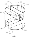
- the dielectric body 200 includes a first end face 201 and a second end face 202 that are opposite to each other and a circumferential surface 203 connected between the first end face 201 and the second end face 202.
- the first end face 201 is provided with a first groove 204
- the second end face 202 is provided with a second groove 206
- the first end face 201 and the second end face 202 are in contact with an inner wall of the conductive housing 100, and extension directions of the first groove 204 and the second groove 206 are different.
- the first groove 204 and the second groove 206 are perpendicularly projected on a same plane, a projection of the first groove 204 intersects a projection of the second groove 206.
- the first end face 201 is in contact with a bottom wall 1011 of the housing 101 of the conductive housing 100
- the second end face 202 is in contact with an inner surface 1021 of the cover 102 of the conductive housing 100
- the inner surface 1021 of the cover 102 is disposed opposite to the bottom wall 1011 of the housing 101.
- the dielectric body 200 of the dielectric resonator is fixed in the conductive housing 100 in an installation manner of crimping the cover 102 on the second end face 202.
- a ground connection relationship is formed both between the first end face 201 and the bottom wall 1011 and between the second end face 202 and the cover 102.
- a conducting layer for example, a metal layer, is disposed on a surface on which the first end face 201 and the second end face 202 are in contact with the conductive housing 100.
- the first end face 201 and the second end face 202 of the dielectric resonator are grounded in a manner in which both the first end face 201 and the second end face 202 are in contact with the inner wall of the conductive housing 100, so that single-sided installation can be implemented and assembly is easy.
- the dielectric body 200 of the dielectric resonator is first placed into the housing 101 of the conductive housing 100, and then, the cover 102 is fixed to the housing 101, and the dielectric body 200 of the dielectric resonator is fixed in the conductive housing 100.
- a conductive elastomer may be disposed between the first end face 201 and the conductive housing 100 or between the second end face 202 and the conductive housing 100, to overcome an installation gap tolerance through elastic deformation of the conductive elastomer, thereby ensuring that the dielectric body 200 of the dielectric resonator is fixed at a position inside the conductive housing 100.
- the dielectric body 200 of the dielectric resonator is in direct contact with the inner wall of the conductive housing 100 through the first end face 201 and the second end face 202, a structure between the dielectric body 200 and the conductive housing 100 is more compact, and there is no excessive hollow space. Therefore, an objective of miniaturization of the filter can be achieved in this application.
- different resonance modes of an electromagnetic field are formed by disposing the first groove 204 and the second groove 206, and a coupling coefficient between the resonance modes can be adjusted because the extension directions of the first groove 204 and the second groove 206 are different.
- first groove 204 and the second groove 206 are different.
- both the first groove 204 and the second groove 206 are strip-shaped, the first groove 204 extends on the first end face 201, the second groove 206 extends on the second end face 202, the first groove 204 and the second groove 206 extend in a direction parallel to the first end face and the second end face, and a direction in which the first groove 204 extends and a direction in which the second groove 206 extends are not parallel.
- extension directions are different described in this specification may be understood as follows:
- the two grooves 204 and 206 are perpendicularly projected on the XY plane, and a projection of the first groove 204 on the XY plane intersects a projection of the second groove 206 on the XY plane to form a specific included angle.
- an intersection point of the projection of the first groove 204 on the XY plane and the projection of the second groove 206 on the XY plane falls within a projection range of the first end face or the second end face on the XY plane.
- extension directions are different described in this specification may alternatively be understood as follows: A projection of the second groove 206 on the first end face 201 intersects with the first groove 204 to form a specific included angle, or a projection of the first groove 204 on the second end face 202 intersects with the second groove 206 to form a specific included angle.
- a coupling bandwidth between modes of the dielectric resonator may be controlled. For example, when the included angle is 90 degrees, coupling approaches 0, and the coupling between two modes may be enhanced by reducing the included angle. Therefore, in this application, the coupling bandwidth can still be flexibly controlled in narrow space, to implement a required operating bandwidth.
- the extension directions of the first groove 204 and the second groove 206 are perpendicular to each other, in other words, the included angle between the extension directions of the first groove 204 and the second groove 206 is close to 90 degrees.
- the being perpendicular to each other described herein in this application may be understood as a state close to being perpendicular, and is not absolutely 90 degrees.
- an angle deviation within a specific range may be tolerated.
- the angle may be any value from 80 degrees to 90 degrees.
- the included angle described in this application is an acute angle or a right angle formed when the extension directions of the first groove and the second groove intersect.
- a range of the included angle may be any value between 0 degrees and 90 degrees, and includes the 90 degrees.
- the first groove 204 and the second groove 206 are crossed to form a dual-mode form.
- the dielectric resonator in this application has a high electric field density, and compared with a dielectric resonator with a same volume, the dielectric resonator in this application has a higher Q value.
- the dielectric body 200 has a central axis A, the central axis A falls on a connection line between a center of the first end face 201 and a center of the second end face 202, and the central axis A passes through the first groove 204 and the second groove 206.
- a central position of the first groove 204 and/or a central position of the second groove 206 falls on the central axis A.
- the central position of the first groove 204 and the central position of the second groove 206 each fall on the central axis A, and the first end face 201 and the second end face 202 of the dielectric resonator in this implementation each form a symmetric structure, and is beneficial for even electric field distribution.
- a same resonance effect can be implemented in any installation direction. Therefore, the dielectric resonator provided in this implementation is easier to install.
- a central position of one of the first groove 204 and the second groove 206 falls on the central axis A, and a central position of the other one deviates from the central axis A.
- notches are formed on the circumferential surface 203 by disposing the first groove 204 and the second groove 206.
- the first groove 204 and the second groove 206 each form two notches on the circumferential surface 203, to be specific, both of two ends of the first groove 204 and two ends of the second groove 206 pass through the circumferential surface 203, so that two orthogonal resonance modes can be formed.
- the first groove 204 may form two notches on the circumferential surface, that is, a first notch 2042 and a second notch 2044.
- the first notch 2042 and the second notch 2044 separately form the two ends of the first groove 204.
- the second groove 206 may also form two notches on the circumferential surface, that is, a third notch 2062 and a fourth notch 2064.
- the third notch 2062 and the fourth notch 2064 separately form the two ends of the second groove 206.
- the first groove 204 may form only one notch on the circumferential surface, in other words, only one end of the first groove 204 extends to the circumferential surface 203, and the other end is cut off on the first end face 201, and no through channel is formed.
- the second groove 206 may also form only one notch on the circumferential surface 203, in other words, only one end of the second groove 206 extends to the circumferential surface 203, and the other end is cut off on the second end face 202, and no through channel is formed.
- the first groove 204 may form no notch on the circumferential surface, in other words, both of the two ends of the first groove 204 are cut off on the first end face 201.
- the second groove 206 may form no notch on the circumferential surface 203, in other words, both of the two ends of the second groove 206 are cut off on the second end face 202.
- a structure such as a protrusion or a partition may be further disposed inside the first groove 204 and/or the second groove 206 based on a requirement.
- a shape of a cross section of the first groove 204 may be a semicircle, a rectangle, a triangle, an irregular shape, or the like.
- the cross section of the first groove 204 refers to a cross section of the first groove 204 that is perpendicular to the extension direction of the first groove 204.
- a shape of a cross section of the second groove 206 may be a semicircle, a rectangle, a trapezoid, a triangle, an irregular shape, or the like. Shapes of cross sections of the first groove 204 and the second groove 206 may be the same or may be different.
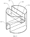
- the dielectric body 200 includes a first side wall 207 and a second side wall 208 that are located in the first groove 204 and a first bottom wall 209 connected between the first side wall 207 and the second side wall 208, and the first side wall 207, the second side wall 208, and the first bottom wall 209 are all of a planar shape.
- the first groove 204 may be a groove of a cuboid shape.
- a cross section of the first groove 204 also needs to be a trapezoid, and the first groove 204 may be formed in a mechanical processing manner.
- a shape of the second groove 206 may be the same as a shape of the first groove 204.
- first side wall 207, the first bottom wall 209, and the second side wall 207 may alternatively be sequentially connected to form a smooth and continuously extending arc surface, for example, similar to a semi-cylindrical surface.
- first groove 204 is of a cylindrical shape, may be prepared by using a die, and is easy to process.
- the dielectric body may be of a cubic shape or a cylindrical shape.
- the circumferential surface of the dielectric body is a cylindrical surface.
- Both the first end face and the second end face are of a planar shape, and both are in direct surface contact with the inner wall of the conductive housing.
- a manner in which planes are directly contacted helps implement a design of miniaturization of the dielectric resonator, and has a good grounding effect.
- the first groove 204 and the second groove 206 are configured to change magnetic field distribution of resonance modes, and control a coupling bandwidth of each resonance mode.
- a coupling coefficient between the resonance modes approaches 0, and coupling is weak coupling.
- a coupling coefficient between the resonance modes approaches the maximum value, and coupling is strong coupling.
- a size of a cross section of the first groove 204 and a size of a cross section of the second groove 206 may be further adjusted, to adjust a change degree of electromagnetic field distribution of the dielectric resonator, and further control coupling strength between the resonance modes.
- first end face 201 and the second end face 202 are of a planar shape, and are in full contact with the inner wall of the conductive housing, that is, in surface contact, thereby implementing a good grounding effect and also simplifying installation.
- the dielectric resonator provided in this application may generate two resonance modes with similar frequencies, and has a basic condition for making a multimode filter.
- the dielectric resonator provided in this application has a high electric field density, and a Q value of the dielectric resonator is about 30% higher than a Q value of a TM single-mode with a same volume.
Landscapes
- Physics & Mathematics (AREA)
- Electromagnetism (AREA)
- Control Of Motors That Do Not Use Commutators (AREA)
Applications Claiming Priority (1)
| Application Number | Priority Date | Filing Date | Title |
|---|---|---|---|
| PCT/CN2017/110868 WO2019095103A1 (fr) | 2017-11-14 | 2017-11-14 | Résonateur diélectrique et filtre |
Publications (3)
| Publication Number | Publication Date |
|---|---|
| EP3675276A1 true EP3675276A1 (fr) | 2020-07-01 |
| EP3675276A4 EP3675276A4 (fr) | 2020-11-11 |
| EP3675276B1 EP3675276B1 (fr) | 2023-07-26 |
Family
ID=66539255
Family Applications (1)
| Application Number | Title | Priority Date | Filing Date |
|---|---|---|---|
| EP17932435.5A Active EP3675276B1 (fr) | 2017-11-14 | 2017-11-14 | Résonateur diélectrique et filtre |
Country Status (4)
| Country | Link |
|---|---|
| US (1) | US11171397B2 (fr) |
| EP (1) | EP3675276B1 (fr) |
| CN (1) | CN111164827B (fr) |
| WO (1) | WO2019095103A1 (fr) |
Families Citing this family (3)
| Publication number | Priority date | Publication date | Assignee | Title |
|---|---|---|---|---|
| CN113782939B (zh) * | 2020-06-09 | 2022-10-28 | 华为技术有限公司 | 一种介质谐振器和滤波器 |
| WO2022120664A1 (fr) * | 2020-12-09 | 2022-06-16 | 华为技术有限公司 | Résonateur diélectrique, filtre diélectrique et station de base |
| CN114039187B (zh) * | 2021-12-03 | 2024-11-15 | 大富科技(安徽)股份有限公司 | 介质双模谐振器及滤波器 |
Family Cites Families (21)
| Publication number | Priority date | Publication date | Assignee | Title |
|---|---|---|---|---|
| CA1194160A (fr) | 1984-05-28 | 1985-09-24 | Wai-Cheung Tang | Filtre bimode a resonateurs dielectriques planar |
| JP2897678B2 (ja) * | 1995-03-22 | 1999-05-31 | 株式会社村田製作所 | 誘電体共振器及び高周波帯域通過フィルタ装置 |
| DE19537477A1 (de) * | 1995-10-09 | 1997-04-10 | Bosch Gmbh Robert | Dielektrischer Resonator sowie Verwendung |
| JPH09148810A (ja) * | 1995-11-20 | 1997-06-06 | Tdk Corp | バンドパスフィルタ装置 |
| JP3503482B2 (ja) * | 1997-09-04 | 2004-03-08 | 株式会社村田製作所 | 多重モード誘電体共振器装置、誘電体フィルタ、複合誘電体フィルタ、合成器、分配器、および通信装置 |
| JP3506077B2 (ja) * | 1999-11-24 | 2004-03-15 | 株式会社村田製作所 | 多重モード誘電体共振器装置、フィルタ、デュプレクサおよび通信装置 |
| EP1363351B1 (fr) * | 2001-01-19 | 2008-08-06 | Matsushita Electric Industrial Co., Ltd. | Element de circuit haute frequence et module de circuit haute frequence |
| GB2465522B (en) * | 2007-09-19 | 2012-02-15 | Ngk Spark Plug Co | Dielectric resonator, dielectric resonator filter and method for controlling dielectric resonator |
| WO2013146494A1 (fr) * | 2012-03-30 | 2013-10-03 | 宇部興産株式会社 | Procédé et dispositif de transmission d'électricité, ainsi que dispositif résonant utilisé dans ceux-ci |
| WO2014024349A1 (fr) * | 2012-08-09 | 2014-02-13 | 日本特殊陶業株式会社 | Résonateur diélectrique en mode tm010, élément de résonateur et filtre diélectrique |
| GB201303024D0 (en) * | 2013-02-21 | 2013-04-03 | Mesaplexx Pty Ltd | Filter |
| KR101468409B1 (ko) * | 2013-11-08 | 2014-12-04 | 주식회사 웨이브일렉트로닉스 | 홈이 파인 도체판을 포함하는 이중 모드 공진기 및 이를 이용한 필터 |
| CN103633402B (zh) * | 2013-12-16 | 2016-08-17 | 华为技术有限公司 | 双工器及具有该双工器的通信系统 |
| CN104577290A (zh) * | 2015-01-29 | 2015-04-29 | 无锡江南计算技术研究所 | 分裂圆柱体谐振腔 |
| KR20160118667A (ko) * | 2015-04-02 | 2016-10-12 | 한국전자통신연구원 | 공진기 필터 |
| WO2017000259A1 (fr) * | 2015-06-30 | 2017-01-05 | 华为技术有限公司 | Résonateur diélectrique et filtre à triple mode |
| CN105406158A (zh) * | 2015-12-29 | 2016-03-16 | 华南理工大学 | 一种基于金属贴片控制频率和耦合的双模介质滤波器 |
| CN106129549B (zh) * | 2016-08-12 | 2019-01-29 | 华南理工大学 | 一种空气腔频率选择表面结构 |
| CN206148591U (zh) * | 2016-08-24 | 2017-05-03 | 张家港保税区灿勤科技有限公司 | 带有金属化矩形柱孔的介质滤波器 |
| CN206225509U (zh) * | 2016-12-02 | 2017-06-06 | 华南理工大学 | 一种新型三模介质带通滤波器 |
| CN107146933A (zh) * | 2017-04-17 | 2017-09-08 | 深圳三星通信技术研究有限公司 | 一种新型tm模双端介子滤波器结构 |
-
2017
- 2017-11-14 WO PCT/CN2017/110868 patent/WO2019095103A1/fr not_active Ceased
- 2017-11-14 CN CN201780095611.0A patent/CN111164827B/zh active Active
- 2017-11-14 EP EP17932435.5A patent/EP3675276B1/fr active Active
-
2020
- 2020-04-29 US US16/861,795 patent/US11171397B2/en active Active
Also Published As
| Publication number | Publication date |
|---|---|
| CN111164827B (zh) | 2021-09-14 |
| CN111164827A (zh) | 2020-05-15 |
| US11171397B2 (en) | 2021-11-09 |
| WO2019095103A1 (fr) | 2019-05-23 |
| EP3675276A4 (fr) | 2020-11-11 |
| US20200259236A1 (en) | 2020-08-13 |
| EP3675276B1 (fr) | 2023-07-26 |
Similar Documents
| Publication | Publication Date | Title |
|---|---|---|
| US11171397B2 (en) | Dielectric resonator and filter | |
| US20120112972A1 (en) | Antenna device | |
| US10164309B2 (en) | Dielectric resonator and dielectric filter | |
| US9859602B2 (en) | Non-reciprocal circuit device and communication apparatus using the same | |
| EP2889950A1 (fr) | Trimmer de phase et amplitude compacte | |
| US20220271410A1 (en) | Resonator apparatus, filter apparatus as well as radio frequency and microwave device | |
| US8368598B2 (en) | Multiband antenna | |
| CN103985933A (zh) | 能够调节传输零点的多重模式滤波器 | |
| CN115411480B (zh) | 一种射频结构、探测装置及通信系统 | |
| ul Haq et al. | Reconfigurable ultra wide band notch filter based on complementary metamaterial | |
| CN109983617B (zh) | 滤波装置 | |
| KR101468409B1 (ko) | 홈이 파인 도체판을 포함하는 이중 모드 공진기 및 이를 이용한 필터 | |
| EP2387096A2 (fr) | Transformateur d'impédance de ligne de transmission et procédés associés | |
| CN111029706A (zh) | 一种耦合器 | |
| JP6629896B2 (ja) | アンテナ装置および該アンテナ装置を用いた測定装置 | |
| US6750730B2 (en) | Tuning arrangement for a microwave device | |
| CN110931933A (zh) | 一种定向耦合器 | |
| CN211655009U (zh) | 环形器 | |
| CN211719758U (zh) | 一种定向耦合器 | |
| JP4572819B2 (ja) | 誘電体共振器および誘電体フィルタ | |
| JP6461039B2 (ja) | 可変特性アンテナ | |
| CN218939977U (zh) | 一种宽带大功率双定向耦合器 | |
| CN218123694U (zh) | 一种同轴定向耦合器 | |
| CN102694227B (zh) | 同轴双模谐振器及滤波器 | |
| KR101052713B1 (ko) | 써큘레이터/아이솔레이터 |
Legal Events
| Date | Code | Title | Description |
|---|---|---|---|
| STAA | Information on the status of an ep patent application or granted ep patent |
Free format text: STATUS: THE INTERNATIONAL PUBLICATION HAS BEEN MADE |
|
| PUAI | Public reference made under article 153(3) epc to a published international application that has entered the european phase |
Free format text: ORIGINAL CODE: 0009012 |
|
| STAA | Information on the status of an ep patent application or granted ep patent |
Free format text: STATUS: REQUEST FOR EXAMINATION WAS MADE |
|
| 17P | Request for examination filed |
Effective date: 20200325 |
|
| AK | Designated contracting states |
Kind code of ref document: A1 Designated state(s): AL AT BE BG CH CY CZ DE DK EE ES FI FR GB GR HR HU IE IS IT LI LT LU LV MC MK MT NL NO PL PT RO RS SE SI SK SM TR |
|
| AX | Request for extension of the european patent |
Extension state: BA ME |
|
| A4 | Supplementary search report drawn up and despatched |
Effective date: 20201008 |
|
| RIC1 | Information provided on ipc code assigned before grant |
Ipc: H01P 7/10 20060101AFI20201002BHEP |
|
| DAV | Request for validation of the european patent (deleted) | ||
| DAX | Request for extension of the european patent (deleted) | ||
| STAA | Information on the status of an ep patent application or granted ep patent |
Free format text: STATUS: EXAMINATION IS IN PROGRESS |
|
| 17Q | First examination report despatched |
Effective date: 20220207 |
|
| GRAP | Despatch of communication of intention to grant a patent |
Free format text: ORIGINAL CODE: EPIDOSNIGR1 |
|
| STAA | Information on the status of an ep patent application or granted ep patent |
Free format text: STATUS: GRANT OF PATENT IS INTENDED |
|
| INTG | Intention to grant announced |
Effective date: 20230214 |
|
| GRAS | Grant fee paid |
Free format text: ORIGINAL CODE: EPIDOSNIGR3 |
|
| GRAA | (expected) grant |
Free format text: ORIGINAL CODE: 0009210 |
|
| STAA | Information on the status of an ep patent application or granted ep patent |
Free format text: STATUS: THE PATENT HAS BEEN GRANTED |
|
| AK | Designated contracting states |
Kind code of ref document: B1 Designated state(s): AL AT BE BG CH CY CZ DE DK EE ES FI FR GB GR HR HU IE IS IT LI LT LU LV MC MK MT NL NO PL PT RO RS SE SI SK SM TR |
|
| REG | Reference to a national code |
Ref country code: CH Ref legal event code: EP |
|
| REG | Reference to a national code |
Ref country code: IE Ref legal event code: FG4D |
|
| REG | Reference to a national code |
Ref country code: DE Ref legal event code: R096 Ref document number: 602017071995 Country of ref document: DE |
|
| REG | Reference to a national code |
Ref country code: LT Ref legal event code: MG9D |
|
| REG | Reference to a national code |
Ref country code: NL Ref legal event code: MP Effective date: 20230726 |
|
| REG | Reference to a national code |
Ref country code: AT Ref legal event code: MK05 Ref document number: 1593014 Country of ref document: AT Kind code of ref document: T Effective date: 20230726 |
|
| PG25 | Lapsed in a contracting state [announced via postgrant information from national office to epo] |
Ref country code: NL Free format text: LAPSE BECAUSE OF FAILURE TO SUBMIT A TRANSLATION OF THE DESCRIPTION OR TO PAY THE FEE WITHIN THE PRESCRIBED TIME-LIMIT Effective date: 20230726 |
|
| PG25 | Lapsed in a contracting state [announced via postgrant information from national office to epo] |
Ref country code: GR Free format text: LAPSE BECAUSE OF FAILURE TO SUBMIT A TRANSLATION OF THE DESCRIPTION OR TO PAY THE FEE WITHIN THE PRESCRIBED TIME-LIMIT Effective date: 20231027 |
|
| PG25 | Lapsed in a contracting state [announced via postgrant information from national office to epo] |
Ref country code: IS Free format text: LAPSE BECAUSE OF FAILURE TO SUBMIT A TRANSLATION OF THE DESCRIPTION OR TO PAY THE FEE WITHIN THE PRESCRIBED TIME-LIMIT Effective date: 20231126 |
|
| PG25 | Lapsed in a contracting state [announced via postgrant information from national office to epo] |
Ref country code: SE Free format text: LAPSE BECAUSE OF FAILURE TO SUBMIT A TRANSLATION OF THE DESCRIPTION OR TO PAY THE FEE WITHIN THE PRESCRIBED TIME-LIMIT Effective date: 20230726 Ref country code: RS Free format text: LAPSE BECAUSE OF FAILURE TO SUBMIT A TRANSLATION OF THE DESCRIPTION OR TO PAY THE FEE WITHIN THE PRESCRIBED TIME-LIMIT Effective date: 20230726 Ref country code: PT Free format text: LAPSE BECAUSE OF FAILURE TO SUBMIT A TRANSLATION OF THE DESCRIPTION OR TO PAY THE FEE WITHIN THE PRESCRIBED TIME-LIMIT Effective date: 20231127 Ref country code: NO Free format text: LAPSE BECAUSE OF FAILURE TO SUBMIT A TRANSLATION OF THE DESCRIPTION OR TO PAY THE FEE WITHIN THE PRESCRIBED TIME-LIMIT Effective date: 20231026 Ref country code: LV Free format text: LAPSE BECAUSE OF FAILURE TO SUBMIT A TRANSLATION OF THE DESCRIPTION OR TO PAY THE FEE WITHIN THE PRESCRIBED TIME-LIMIT Effective date: 20230726 Ref country code: LT Free format text: LAPSE BECAUSE OF FAILURE TO SUBMIT A TRANSLATION OF THE DESCRIPTION OR TO PAY THE FEE WITHIN THE PRESCRIBED TIME-LIMIT Effective date: 20230726 Ref country code: IS Free format text: LAPSE BECAUSE OF FAILURE TO SUBMIT A TRANSLATION OF THE DESCRIPTION OR TO PAY THE FEE WITHIN THE PRESCRIBED TIME-LIMIT Effective date: 20231126 Ref country code: HR Free format text: LAPSE BECAUSE OF FAILURE TO SUBMIT A TRANSLATION OF THE DESCRIPTION OR TO PAY THE FEE WITHIN THE PRESCRIBED TIME-LIMIT Effective date: 20230726 Ref country code: GR Free format text: LAPSE BECAUSE OF FAILURE TO SUBMIT A TRANSLATION OF THE DESCRIPTION OR TO PAY THE FEE WITHIN THE PRESCRIBED TIME-LIMIT Effective date: 20231027 Ref country code: FI Free format text: LAPSE BECAUSE OF FAILURE TO SUBMIT A TRANSLATION OF THE DESCRIPTION OR TO PAY THE FEE WITHIN THE PRESCRIBED TIME-LIMIT Effective date: 20230726 Ref country code: AT Free format text: LAPSE BECAUSE OF FAILURE TO SUBMIT A TRANSLATION OF THE DESCRIPTION OR TO PAY THE FEE WITHIN THE PRESCRIBED TIME-LIMIT Effective date: 20230726 |
|
| PG25 | Lapsed in a contracting state [announced via postgrant information from national office to epo] |
Ref country code: PL Free format text: LAPSE BECAUSE OF FAILURE TO SUBMIT A TRANSLATION OF THE DESCRIPTION OR TO PAY THE FEE WITHIN THE PRESCRIBED TIME-LIMIT Effective date: 20230726 |
|
| PG25 | Lapsed in a contracting state [announced via postgrant information from national office to epo] |
Ref country code: ES Free format text: LAPSE BECAUSE OF FAILURE TO SUBMIT A TRANSLATION OF THE DESCRIPTION OR TO PAY THE FEE WITHIN THE PRESCRIBED TIME-LIMIT Effective date: 20230726 |
|
| REG | Reference to a national code |
Ref country code: DE Ref legal event code: R097 Ref document number: 602017071995 Country of ref document: DE |
|
| PG25 | Lapsed in a contracting state [announced via postgrant information from national office to epo] |
Ref country code: SM Free format text: LAPSE BECAUSE OF FAILURE TO SUBMIT A TRANSLATION OF THE DESCRIPTION OR TO PAY THE FEE WITHIN THE PRESCRIBED TIME-LIMIT Effective date: 20230726 Ref country code: RO Free format text: LAPSE BECAUSE OF FAILURE TO SUBMIT A TRANSLATION OF THE DESCRIPTION OR TO PAY THE FEE WITHIN THE PRESCRIBED TIME-LIMIT Effective date: 20230726 Ref country code: ES Free format text: LAPSE BECAUSE OF FAILURE TO SUBMIT A TRANSLATION OF THE DESCRIPTION OR TO PAY THE FEE WITHIN THE PRESCRIBED TIME-LIMIT Effective date: 20230726 Ref country code: EE Free format text: LAPSE BECAUSE OF FAILURE TO SUBMIT A TRANSLATION OF THE DESCRIPTION OR TO PAY THE FEE WITHIN THE PRESCRIBED TIME-LIMIT Effective date: 20230726 Ref country code: DK Free format text: LAPSE BECAUSE OF FAILURE TO SUBMIT A TRANSLATION OF THE DESCRIPTION OR TO PAY THE FEE WITHIN THE PRESCRIBED TIME-LIMIT Effective date: 20230726 Ref country code: CZ Free format text: LAPSE BECAUSE OF FAILURE TO SUBMIT A TRANSLATION OF THE DESCRIPTION OR TO PAY THE FEE WITHIN THE PRESCRIBED TIME-LIMIT Effective date: 20230726 Ref country code: SK Free format text: LAPSE BECAUSE OF FAILURE TO SUBMIT A TRANSLATION OF THE DESCRIPTION OR TO PAY THE FEE WITHIN THE PRESCRIBED TIME-LIMIT Effective date: 20230726 |
|
| PG25 | Lapsed in a contracting state [announced via postgrant information from national office to epo] |
Ref country code: IT Free format text: LAPSE BECAUSE OF FAILURE TO SUBMIT A TRANSLATION OF THE DESCRIPTION OR TO PAY THE FEE WITHIN THE PRESCRIBED TIME-LIMIT Effective date: 20230726 |
|
| PLBE | No opposition filed within time limit |
Free format text: ORIGINAL CODE: 0009261 |
|
| STAA | Information on the status of an ep patent application or granted ep patent |
Free format text: STATUS: NO OPPOSITION FILED WITHIN TIME LIMIT |
|
| REG | Reference to a national code |
Ref country code: CH Ref legal event code: PL |
|
| PG25 | Lapsed in a contracting state [announced via postgrant information from national office to epo] |
Ref country code: MC Free format text: LAPSE BECAUSE OF FAILURE TO SUBMIT A TRANSLATION OF THE DESCRIPTION OR TO PAY THE FEE WITHIN THE PRESCRIBED TIME-LIMIT Effective date: 20230726 |
|
| 26N | No opposition filed |
Effective date: 20240429 |
|
| PG25 | Lapsed in a contracting state [announced via postgrant information from national office to epo] |
Ref country code: LU Free format text: LAPSE BECAUSE OF NON-PAYMENT OF DUE FEES Effective date: 20231114 |
|
| PG25 | Lapsed in a contracting state [announced via postgrant information from national office to epo] |
Ref country code: CH Free format text: LAPSE BECAUSE OF NON-PAYMENT OF DUE FEES Effective date: 20231130 |
|
| GBPC | Gb: european patent ceased through non-payment of renewal fee |
Effective date: 20231114 |
|
| PG25 | Lapsed in a contracting state [announced via postgrant information from national office to epo] |
Ref country code: MC Free format text: LAPSE BECAUSE OF FAILURE TO SUBMIT A TRANSLATION OF THE DESCRIPTION OR TO PAY THE FEE WITHIN THE PRESCRIBED TIME-LIMIT Effective date: 20230726 Ref country code: LU Free format text: LAPSE BECAUSE OF NON-PAYMENT OF DUE FEES Effective date: 20231114 Ref country code: CH Free format text: LAPSE BECAUSE OF NON-PAYMENT OF DUE FEES Effective date: 20231130 Ref country code: SI Free format text: LAPSE BECAUSE OF FAILURE TO SUBMIT A TRANSLATION OF THE DESCRIPTION OR TO PAY THE FEE WITHIN THE PRESCRIBED TIME-LIMIT Effective date: 20230726 |
|
| REG | Reference to a national code |
Ref country code: BE Ref legal event code: MM Effective date: 20231130 |
|
| REG | Reference to a national code |
Ref country code: IE Ref legal event code: MM4A |
|
| PG25 | Lapsed in a contracting state [announced via postgrant information from national office to epo] |
Ref country code: IE Free format text: LAPSE BECAUSE OF NON-PAYMENT OF DUE FEES Effective date: 20231114 |
|
| PG25 | Lapsed in a contracting state [announced via postgrant information from national office to epo] |
Ref country code: GB Free format text: LAPSE BECAUSE OF NON-PAYMENT OF DUE FEES Effective date: 20231114 |
|
| PG25 | Lapsed in a contracting state [announced via postgrant information from national office to epo] |
Ref country code: BE Free format text: LAPSE BECAUSE OF NON-PAYMENT OF DUE FEES Effective date: 20231130 |
|
| PG25 | Lapsed in a contracting state [announced via postgrant information from national office to epo] |
Ref country code: FR Free format text: LAPSE BECAUSE OF NON-PAYMENT OF DUE FEES Effective date: 20231130 |
|
| PG25 | Lapsed in a contracting state [announced via postgrant information from national office to epo] |
Ref country code: IE Free format text: LAPSE BECAUSE OF NON-PAYMENT OF DUE FEES Effective date: 20231114 Ref country code: GB Free format text: LAPSE BECAUSE OF NON-PAYMENT OF DUE FEES Effective date: 20231114 Ref country code: FR Free format text: LAPSE BECAUSE OF NON-PAYMENT OF DUE FEES Effective date: 20231130 Ref country code: BE Free format text: LAPSE BECAUSE OF NON-PAYMENT OF DUE FEES Effective date: 20231130 |
|
| PG25 | Lapsed in a contracting state [announced via postgrant information from national office to epo] |
Ref country code: BG Free format text: LAPSE BECAUSE OF FAILURE TO SUBMIT A TRANSLATION OF THE DESCRIPTION OR TO PAY THE FEE WITHIN THE PRESCRIBED TIME-LIMIT Effective date: 20230726 |
|
| PG25 | Lapsed in a contracting state [announced via postgrant information from national office to epo] |
Ref country code: BG Free format text: LAPSE BECAUSE OF FAILURE TO SUBMIT A TRANSLATION OF THE DESCRIPTION OR TO PAY THE FEE WITHIN THE PRESCRIBED TIME-LIMIT Effective date: 20230726 |
|
| PG25 | Lapsed in a contracting state [announced via postgrant information from national office to epo] |
Ref country code: CY Free format text: LAPSE BECAUSE OF FAILURE TO SUBMIT A TRANSLATION OF THE DESCRIPTION OR TO PAY THE FEE WITHIN THE PRESCRIBED TIME-LIMIT; INVALID AB INITIO Effective date: 20171114 |
|
| PG25 | Lapsed in a contracting state [announced via postgrant information from national office to epo] |
Ref country code: HU Free format text: LAPSE BECAUSE OF FAILURE TO SUBMIT A TRANSLATION OF THE DESCRIPTION OR TO PAY THE FEE WITHIN THE PRESCRIBED TIME-LIMIT; INVALID AB INITIO Effective date: 20171114 |
|
| PG25 | Lapsed in a contracting state [announced via postgrant information from national office to epo] |
Ref country code: TR Free format text: LAPSE BECAUSE OF FAILURE TO SUBMIT A TRANSLATION OF THE DESCRIPTION OR TO PAY THE FEE WITHIN THE PRESCRIBED TIME-LIMIT Effective date: 20230726 |
|
| PGFP | Annual fee paid to national office [announced via postgrant information from national office to epo] |
Ref country code: DE Payment date: 20250930 Year of fee payment: 9 |