EP3675355B1 - Digitaler hüllkurvenverfolger für leistungsverstärker - Google Patents
Digitaler hüllkurvenverfolger für leistungsverstärker Download PDFInfo
- Publication number
- EP3675355B1 EP3675355B1 EP18248077.2A EP18248077A EP3675355B1 EP 3675355 B1 EP3675355 B1 EP 3675355B1 EP 18248077 A EP18248077 A EP 18248077A EP 3675355 B1 EP3675355 B1 EP 3675355B1
- Authority
- EP
- European Patent Office
- Prior art keywords
- switching
- level
- supply
- filter
- events
- Prior art date
- Legal status (The legal status is an assumption and is not a legal conclusion. Google has not performed a legal analysis and makes no representation as to the accuracy of the status listed.)
- Active
Links
Images




Classifications
-
- H—ELECTRICITY
- H03—ELECTRONIC CIRCUITRY
- H03F—AMPLIFIERS
- H03F1/00—Details of amplifiers with only discharge tubes, only semiconductor devices or only unspecified devices as amplifying elements
- H03F1/02—Modifications of amplifiers to raise the efficiency, e.g. gliding Class A stages, use of an auxiliary oscillation
- H03F1/0205—Modifications of amplifiers to raise the efficiency, e.g. gliding Class A stages, use of an auxiliary oscillation in transistor amplifiers
- H03F1/0211—Modifications of amplifiers to raise the efficiency, e.g. gliding Class A stages, use of an auxiliary oscillation in transistor amplifiers with control of the supply voltage or current
- H03F1/0216—Continuous control
-
- H—ELECTRICITY
- H03—ELECTRONIC CIRCUITRY
- H03F—AMPLIFIERS
- H03F1/00—Details of amplifiers with only discharge tubes, only semiconductor devices or only unspecified devices as amplifying elements
- H03F1/02—Modifications of amplifiers to raise the efficiency, e.g. gliding Class A stages, use of an auxiliary oscillation
- H03F1/0205—Modifications of amplifiers to raise the efficiency, e.g. gliding Class A stages, use of an auxiliary oscillation in transistor amplifiers
- H03F1/0211—Modifications of amplifiers to raise the efficiency, e.g. gliding Class A stages, use of an auxiliary oscillation in transistor amplifiers with control of the supply voltage or current
- H03F1/0244—Stepped control
- H03F1/025—Stepped control by using a signal derived from the input signal
-
- H—ELECTRICITY
- H03—ELECTRONIC CIRCUITRY
- H03F—AMPLIFIERS
- H03F1/00—Details of amplifiers with only discharge tubes, only semiconductor devices or only unspecified devices as amplifying elements
- H03F1/02—Modifications of amplifiers to raise the efficiency, e.g. gliding Class A stages, use of an auxiliary oscillation
- H03F1/0205—Modifications of amplifiers to raise the efficiency, e.g. gliding Class A stages, use of an auxiliary oscillation in transistor amplifiers
- H03F1/0211—Modifications of amplifiers to raise the efficiency, e.g. gliding Class A stages, use of an auxiliary oscillation in transistor amplifiers with control of the supply voltage or current
- H03F1/0216—Continuous control
- H03F1/0222—Continuous control by using a signal derived from the input signal
- H03F1/0227—Continuous control by using a signal derived from the input signal using supply converters
-
- H—ELECTRICITY
- H03—ELECTRONIC CIRCUITRY
- H03F—AMPLIFIERS
- H03F3/00—Amplifiers with only discharge tubes or only semiconductor devices as amplifying elements
- H03F3/189—High-frequency amplifiers, e.g. radio frequency amplifiers
- H03F3/19—High-frequency amplifiers, e.g. radio frequency amplifiers with semiconductor devices only
-
- H—ELECTRICITY
- H03—ELECTRONIC CIRCUITRY
- H03F—AMPLIFIERS
- H03F3/00—Amplifiers with only discharge tubes or only semiconductor devices as amplifying elements
- H03F3/20—Power amplifiers, e.g. Class B amplifiers, Class C amplifiers
- H03F3/21—Power amplifiers, e.g. Class B amplifiers, Class C amplifiers with semiconductor devices only
-
- H—ELECTRICITY
- H03—ELECTRONIC CIRCUITRY
- H03F—AMPLIFIERS
- H03F2200/00—Indexing scheme relating to amplifiers
- H03F2200/105—A non-specified detector of the power of a signal being used in an amplifying circuit
-
- H—ELECTRICITY
- H03—ELECTRONIC CIRCUITRY
- H03F—AMPLIFIERS
- H03F2200/00—Indexing scheme relating to amplifiers
- H03F2200/171—A filter circuit coupled to the output of an amplifier
Definitions
- Examples relate to a digital envelop tracker for a power amplifier, more particularly a digital envelop tracker with a low loss supply filter for the radio frequency (RF) power amplifier and with lower peaking.
- RF radio frequency
- Envelope tracking is a scheme to adjust a supply voltage to an RF power amplifier to ensure that the RF power amplifier operates close to its peak efficiency.
- digital envelope tracking the supply voltage to the RF power amplifier is discrete voltage levels.
- the envelope tracker switches stepwise between these discrete voltage levels depending on the instantaneous RF power of an input data stream.
- a supply filter e.g. a passive filter
- This supply filter needs to have low losses because any loss in the supply filter reduces the efficiency of the overall envelope tracking.
- the step response of the supply filter needs to not peak much because the peaking would lead to a violation of the maximum voltage requirement of the power amplifier. The two requirements are contradictory because a lossless LC filter does peak and ring.
- US 2016/0099686 Aldiscloses a radio frequency amplifier system having at least one amplifier.
- the at least one amplifier includes an RF input port, an RF output port and a drain bias port.
- At least one voltage modulator is coupled to the bias port of the least one amplifier to provide a bias voltage.
- the bias voltage is selected by switching among a plurality of discrete voltages.
- At least one filter circuit is coupled between the at least one voltage modulator and the at least one amplifier. The at least one filter circuit controls spectral components resultant from transitions in the bias voltage when switching among the plurality of discrete voltages.
- a snubber network which is a capacitor in series with a resistor, may be used.
- the resistor in the snubber network dissipates the ringing energy so reduces the peaking. Peaking is reduced by burning the energy.
- this scheme increases alternating current (AC) losses in the supply filter so that the efficiency of the digital envelope tracker decreases.
- Examples are disclosed for a digital envelop tracker with a low-loss and high-Q supply filter for the RF power amplifier and with lower peaking so as not to violate the maximum voltage requirement of the RF power amplifier.
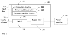
- Fig. 1 is a block diagram of a digital envelop tracker 100 in accordance with one example.
- the digital envelop tracker 100 may include a level selection circuitry 110, a switch 120, and a supply filter 130.
- the supply filter 130 is configured to filter a supply voltage 104 supplied to a power amplifier 140.
- the supply voltages 104 are discrete voltage levels and the envelope tracker 100 switches stepwise between these discrete voltage levels depending on the instantaneous RF power of an input data stream 102.
- the supply filter 130 between the switch 120 and an input of the power amplifier 140 is used to smoothen the transition of the supply voltage from one level to another.
- the supply filter 130 may be a passive filter.
- the level selection circuitry 110 is configured to determine a level of the supply voltage based on an instantaneous RF power of an input data stream 102, schedule a series of switching events of the switch 120 based on the determined level of supply voltage, and generate a level select signal 160.
- the instantaneous RF power measurement is an instantaneous power prediction ahead in time.
- the instantaneous power is not necessarily the power required at the current time instance but is the value slightly in the future.
- the switch 120 is configured to connect one of a plurality of supply voltages 104 in different levels to the supply filter 130 based on the level select signal 160.
- the level select signal 160 may trigger an increase, a decrease, or no change of the supply voltage from the current supply voltage level.
- the switch 120 switches to a higher or lower level or does not change based on the level select signal 160.
- the level selection circuitry 110 is configured to schedule a series of switching events of the switch 120 based on the determined level of supply voltage.
- the level selection circuitry 110 includes a primary switching circuitry 111 and a secondary switching circuitry.
- the primary switching circuitry 111 is configured to initiate primary switching events based on the instantaneous power of the input data stream 102 and the secondary switching circuitry 112 is configured to schedule secondary (i.e. delayed, derived) switching events of the switch 120 in response to the primary switching events.
- the primary switching event is a switching event of the switch 120 scheduled based on the instantaneous power of the input data stream.
- the secondary switching event is switching events of the switch 120 scheduled in response to the primary switching event after predetermined periods of time from the primary switching. For example, if a primary switching event is scheduled for up-switching, the secondary switching events may be down-switching followed by up-switching after certain period of times, respectively.
- the secondary switching circuitry 112 is configured to cause the secondary switching at time instances after the primary switching to generate a filter response of the supply filter 130 with smaller peaking (i.e. smaller overshoots or undershoots).
- the secondary switching circuitry 112 translates the switch selection event (i.e. the primary switching) into a train of switching events. Since the supply voltages 104 are discrete voltage levels one of which is switched by the switch 120 the supply voltage abruptly changes when the switch 120 switches from one voltage level to another. This causes a step response of the supply filter 130.
- a step response is a transient response (behavior) of a system (e.g. the supply filter 130) to a step input.
- a typical step response of the system is a damped oscillation where the output of the system oscillates until it reaches a steady state.
- the train of switching events are chosen such that the output signal from the supply filter 130 is an advantageous superposition of multiple filter step responses which effectively leads to a filter response with much smaller peaking.
- low peaking at the output of the supply filter 130 i.e. at the supply pin of the power amplifier 140
- a snubber resistor This reduces the power consumption in the supply filter 130 and so increases the efficiency of digital envelope tracking.
- a simpler supply filter topology is possible.
- Fig. 2 shows a digital envelop tracker 100 in accordance with the claimed invention.
- the digital envelop tracker 100 includes a level selection circuitry 110, a switch 120, and a supply filter 130.
- the digital envelop tracker 100 may include a clamping device (e.g. a clamping diode 150) for limiting the output voltage from the supply filter 130 for safety reasons.
- a clamping device e.g. a clamping diode 150
- one of six voltage levels is supplied to the supply filter 130 via the switch 120. It should be noted that the configuration shown in Fig. 2 is merely an example, and the number of supply voltage levels may be more or less than 6 and may be any number.
- the supply filter 130 filters the supply voltage 104 provided through the switch 120 and then provides the filtered supply voltage to a power amplifier.
- the supply filter 130 may be configured to pass or reject specific frequency band and may be used for extracting a specific frequency band or rejecting for noise reduction.
- the supply filter 130 may be an LC filter comprising an inductor(s) and a capacitor(s).
- the supply filter 130 may include cascaded inductor-capacitor networks.
- the supply filter 130 includes a series inductor and a shunt capacitor.
- the supply filter 130 may not include a snubber resistance, as shown in Fig. 2 , so that peaking might occur but AC power dissipation would be reduced.
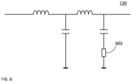
- the supply filter 130 may include small snubber resistance.
- Fig. 6 shows an example supply filter with a snubber resistance 602.
- the level selection circuitry 110 determines a level of the supply voltage based on an instantaneous RF power of an input data stream and outputs the level select signal 160 to the switch 120. In this example in Fig. 2 , one of six voltage levels is selected based on the level select signal 160.
- Fig. 3 shows details of a level selection circuitry 110 in accordance with the claimed invention.
- the level selection circuitry 110 may be part of a transceiver or tracker chip.
- the level selection circuitry 110 may include a primary switching circuitry 111, a secondary switching circuitry 112, and a combiner 118.
- the primary switching circuitry 111 receives input data stream 102, determines a level of the supply voltage for the power amplifier based on an instantaneous RF power of the input data stream 102, and determines a primary switching event.
- the input data stream 102 may be in an in-phase/quadrature (I/Q) format (i.e. Cartesian coordinate format) or alternatively in a polar coordinate format.
- the input data stream 102 (e.g. IQ signals) determines which level needs to be used to give enough power supply headroom to the power amplifier 140.
- the primary switching circuitry 111 determines whether the currently supplied voltage level should be increased or decreased.
- the increase or decrease may be step-wise.
- the primary switching circuitry 111 may output one of an integer value -N,...,-1, 0, +1,...,+N for decrease, no change, or increase of the currently supply voltage level.
- the increase or decrease of the supply voltage level may be one step or multiple steps of increase or decrease.
- the level selection circuitry 110 may include a threshold detector.
- the data stream coming in (e.g. as IQ data) is converted to a magnitude value that represents the instantaneous magnitude of the RF signal.
- This magnitude value may be compared against thresholds and based on this comparison the most appropriate voltage level may be chosen, (e.g. the smallest voltage level which is larger than the magnitude value). This determination is done a little bit forward looking, (i.e. when the magnitude is supposed to get larger than a certain threshold), and then the respective voltage level is selected.
- the primary switching events are determined based on the threshold comparison and the primary switching events are extended by secondary (derived) switching events.
- the primary switching circuitry 111 may fill voltage level increase and decrease events (or commands) into loading logic 116a/116b (e.g. a scheduler) based on forward looking comparison of the input data magnitude with input data magnitude threshold levels.
- the loading logic 116a/116b may schedule and trigger future voltage level increase and decrease events.
- the scheduler may include a first scheduler configured to schedule and trigger future voltage level increase events/commands and a second scheduler configured to schedule and trigger future voltage level decrease events/commands.
- the primary switching circuitry (the threshold detector) may fill voltage level increase events/commands into the first scheduler and voltage level decrease events/commands into the second scheduler based on forward looking comparison of the input data magnitude with input data magnitude threshold levels.
- the combiner 118 may combine the level increase events from the first scheduler and the voltage level decrease events from the second scheduler into a voltage level selection signal.
- This primary switching event may trigger scheduling of secondary (delayed) switching events.
- the secondary switching circuitry 112 may cause the secondary switching events in response to the primary switching event.
- the secondary switching event is a switching event derived from the primary switching event to cause the switch 120 to transition to different levels after predetermined delayed periods from the primary switching.
- the secondary switching events are scheduled and stored, for example, in a shift register or alternatively in a task list. After the delay time the secondary switching events are combined with the then-current primary switching events in the combiner 118 to generate the level select signal 160.
- the series of switching events may be scheduled such that a first step response of the supply filter 130 is combined with second and third step responses of the supply filter 130 such that a steady state value of combination of step responses is equal to a steady state value of the first step response and peaking of the combination of step responses is less than peaking of the first step response.
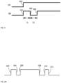
- Fig. 4A shows an example of primary switching without secondary (delayed) switching
- Fig. 4B shows an example of primary switching with secondary (delayed) switching
- the switching events are provided as a pulse train.
- the rising edge indicates incremental switching in which the switch 120 will switch to a higher level of supply voltage and the falling edge indicates decremental switching in which the switch 120 will switch to a lower level of supply voltage.
- the primary switching event 402 is an incremental switching.
- the first secondary switching event 404 occurs at a first delay time (T1) after the primary switching event 402 and a second secondary switching event 406 occurs at a second delay time (T2) after the first secondary switching event 404.
- Both the first and second secondary switching events 404, 406 are derived from the primary switching event 402.
- Fig. 4B shows two secondary switching events 404, 406 derived from the primary switching event 402, but as an alternative, more than two secondary switching events may be scheduled. The examples disclosed herein are explained with reference to the case that two secondary switching events are scheduled, but the examples are not limited to such case, and may be extended to a case with three or more secondary switching events.
- Fig. 4B shows that the amount of changes of the supply voltages in the secondary switching 404, 406 are the same as the amount of change in the primary switching 402 (e.g. one step up in the primary switching 402, one step down in the first secondary switching 404 and one step up in the second secondary switching 406).
- the amount of changes in the secondary switching 404, 406 may be different from the amount of change in the primary switching 402 (e.g. one step up in the primary switching 402, two steps down in the first secondary switching 404 and two steps up in the second secondary switching 406).
- the switch 120 for the level selection may be switched forth-back-forth (i.e. increment-decrement-increment).
- the secondary switching may yield a superposition of two positive step responses and one negative step response which can cancel out the peaks in the step response of the supply filter 130.
- the train of switching may be back-forth-back (i.e. decrement-increment-decrement).
- the secondary switching circuitry 112 may cause the secondary switching events at time instances after the primary switching event to generate a filter response of the supply filter 130 with smaller peaking.
- the secondary switching events are chosen such that the output signal from the supply filter 130 is an advantageous superposition of multiple filter step responses which effectively leads to a filter response with much smaller peaking.
- the secondary switching events may be scheduled and stored, e.g. in a shift register or alternatively in a task list, or the like.
- the secondary switching circuitry 112 may include an increment shift register 114a to store a secondary switching event for increment and a decrement shift register 114b to store a secondary switching event for decrement.
- Fig. 5A shows examples of delayed switching events as pulse train.
- the switching events 502 and 508 are the regular primary switching events determined based on the instantaneous power level of the input data stream.
- the primary switching event 502, 508 may be an incremental switching or a decremental switching.
- the switching events 504 and 512 are secondary switching events derived from the primary switching events 502 and 508, respectively, to be stored in the decrement shift register 114b.
- the switching events 506 and 510 are secondary switching events derived from the primary switching events 502 and 508, respectively, to be stored in the increment shift register 114a.
- Figs. 5B and 5C show examples of two primary switching events and their secondary switching events and the result of overlapping.
- the top two rows of Fig. 5B show the first and second primary switching events which are followed by secondary switching events derived from each primary switching event, respectively.
- the third row of Fig. 5B shows the overlapping result of the two primary switching events and their secondary switching events.
- Fig. 5C shows another example of two primary switching events and the secondary switching events and the overlapping result.
- the loading logic 116a, 116b for shift register loads the secondary switching events to the shift register 114a, 114b, respectively, in response to the primary switching event.
- the secondary switching events are loaded to the shift registers 114a, 114b for the delay time T1 and T2.
- the secondary switching events are shifted along the shift register 114a, 114b at each clock and after the delay time (e.g. T1 and T2, respectively) those previously scheduled secondary switching events are combined with the then-current primary switching event in the combiner 118 to determine the new supply voltage level (i.e. the level select signal 160) which needs to be switched to the supply filter 130.
- the level selection circuitry 110 may include an integrator 119 (e.g. a loop filter) for integrating the outputs of the combiner 118 before generating the level select signal 160 to the switch 120.
- an integrator 119 e.g. a loop filter
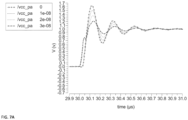
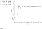
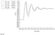
- Figs. 7A-7C show step responses of the supply filter 130 for different delay times (T1) in one example.
- Figs. 7A-7C show step responses of the supply filter 130 with varying T1 while T2 is fixed as an example.
- Figs. 7A-7C are an example for showing that how the choice of the delay time T1 and T2 influences the step response of the supply filter 130.
- T1 and T2 which is filter specific, the supply filter 130 may show a step response with very low peaking even without snubber resistance. In the example of Figs. 7A-7C , the peaking is lowest at T1 of 10 -8 second. Since the proper delay times T1 and T2 are filter specific, different values of T1 and T2 should be selected for different supply filter structure.
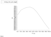
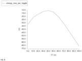
- Fig. 9 shows an example of energy loss of a single up-down switching pulse over time T1 in case no snubber resistor is used.
- a clamping device e.g. a diode
- Fig. 2 shows the clamping diode 150 connected between the output of the supply filter 130 and the highest supply voltage 104. If the peaking is too high the diode 150 clamps the voltage level to a value that does not damage the power amplifier 140.
- a peak detector 170 may be connected to the output of the supply filter 130, i.e. to the input of the power amplifier or to an intermediate node of the supply filter 130.
- the peak detector 170 may measure the peaks and provide a peak measurement signal representing an amount of peaking of a step response of the supply filter 130.
- a calibration circuitry 172 may adjust the delay times T1 and/or T2 continuously (and automatically) to get the lowest peaking and so the lowest power consumption.
- the calibration circuitry 172 may tune the first delay time and/or the second delay time based on the peak measurement signal in a direction which reduces the peaking of the step response of the supply filer.
- Fig. 11 shows a digital envelop tracker including a peak detector 170 and a calibration circuitry 172 in accordance with one example.
- the voltage peaking at the output of the PA supply filter depends on the settings of the delay times T1 and T2.
- the components in the PA supply filter 130 and the power amplifier 140 may vary (e.g. inductances L, capacitances C, or resistors R) from part to part, over time, over voltage, and/or over temperature, the times T1 and T2 may vary too. For this reason a peak detector 170 may be attached to the output of the PA supply filter 130.
- the peak detector 170 may be an ADC which measures the peak in a single shot, an iterative ADC or a threshold detector with a tunable threshold (e.g. a comparator with a tunable threshold). The peak detector 170 measures whether a certain peaking level has been reached or it quantifies as peaking in a digital representation. The peak detector 170 provides the actual peak digits to the calibration circuitry 172.
- the calibration circuitry 172 (an optimizer) may also receive a target value for the peak (a programmable peak target or threshold) and try to minimize the peak or to make the peak equal to the provided peak target.
- the calibration circuitry 172 may adjust the times T1 and T2 such that the optimization goal is met.
- the calibration circuitry 172 may iteratively calculate ⁇ T1 and ⁇ T2 for increase or decrease of T1 and T2 and calculates T1 and T2 with a loop filter 173.
- the calibration circuitry 172 then provides the adjusted T1 and T2 values to the level selection circuitry 110 (e.g. to the loading logics 116a/116b).
- the actual T1 and T2 values which are provided to the loading logics 116a/116b (schedulers)) may be continuously increased or decreased.
- the tuning of the times T1 and T2 may be done either continuously in order to adapt permanently to the actual conditions or periodically, i.e. from time to time when a significant change is expected.
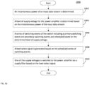
- Fig. 10 is a flow diagram of a process of digital envelop tracking and controlling a supply voltage to a power amplifier in accordance with one example.
- An instantaneous power of an input data stream is determined (1002).
- a level of supply voltage for the power amplifier is determined based on the instantaneous power of the input data stream (1004).
- a series of switching events of the switch including a primary switching event and secondary switching events are scheduled based on the determined level of supply voltage (1006).
- the primary switching event is scheduled based on the determined level of supply voltage and the secondary switching events are scheduled with respect to the primary switching event based on the determined level of supply voltage.
- a level select signal is generated based on the scheduled series of switching events (1008).
- the scheduled switching events are combined to generate the level select signal for the switch.
- One of the supply voltages is switched to the power amplifier via a supply filter based on the level select signal (1010).
- Another example is a computer program having a program code for performing at least one of the methods described herein, when the computer program is executed on a computer, a processor, or a programmable hardware component.
- Another example is a machine-readable storage including machine readable instructions, when executed, to implement a method or realize an apparatus as described herein.
- a further example is a machine-readable medium including code, when executed, to cause a machine to perform any of the methods described herein.
Landscapes
- Engineering & Computer Science (AREA)
- Power Engineering (AREA)
- Amplifiers (AREA)
Claims (8)
- Digitaler Hüllkurvenverfolger (100), umfassend:einen Versorgungsfilter (130), der dazu ausgelegt ist,eine Versorgungsspannung zu filtern;eine Pegelauswahlschaltung (110), die dazu ausgelegt ist,einen Pegel der Versorgungsspannung basierend auf einer Momentanleistung eines Eingangsdatenstroms zu bestimmen,eine Reihe von Schaltereignissen basierend auf dem bestimmten Pegel der Versorgungsspannung zu planen undein Pegelauswahlsignal (160) basierend auf der geplanten Reihe von Schaltereignissen zu erzeugen;einen Schalter (120), der dazu ausgelegt ist, eine aus einer Mehrzahl von Versorgungsspannungen in verschiedenen Pegeln mit dem Versorgungsfilter basierend auf dem Pegelauswahlsignal zu verbinden, wobei die Pegelauswahlschaltung umfasst:einen primären Schaltkreis (111), die dazu ausgelegt ist,ein primäres Schaltereignis des Schalters (120) basierend auf dem bestimmten Pegel der Versorgungsspannung zu planen;einen sekundären Schaltkreis (112), die dazu ausgelegt ist, sekundäre Schaltereignisse des Schalters (120) zu Zeitpunkten zu planen, die gegenüber dem primären Schaltereignis basierend auf dem bestimmten Pegel der Versorgungsspannung verzögert sind;einen Kombinierer (118), der dazu ausgelegt ist, das primäre Schaltereignis und zuvor geplante sekundäre Schaltereignisse zu kombinieren, um das Pegelauswahlsignal (160) zu erzeugen,wobei das sekundäre Schalten ein erstes sekundäres Schalten zu einer ersten Verzögerungszeit von dem primären Schalten in einer entgegengesetzten Richtung von dem primären Schalten und ein zweites sekundäres Schalten zu einer zweiten Verzögerungszeit von dem ersten sekundären Schalten in einer gleichen Richtung wie das primäre Schalten beinhaltet,wobei die erste Verzögerungszeit und die zweite Verzögerungszeit basierend auf einer Sprungantwort des Versorgungsfilters (130) bestimmt werden; und wobei der digitale Hüllkurvenverfolger umfasst:einen Spitzenwertdetektor, der dazu ausgelegt ist, ein Spitzenwert-Messsignal bereitzustellen, das das Ausmaß des Spitzenwertes einer Sprungantwort des Versorgungsfilters repräsentiert;eine Kalibrierungsschaltung, die dazu ausgelegt ist, die erste Verzögerungszeit und/oder die zweite Verzögerungszeit basierend auf dem Spitzenmesssignal in einer Richtung abzustimmen, die den Spitzenwert der Sprungantwort des Versorgungsfilters reduziert.
- Digitaler Hüllkurvenverfolger nach Anspruch 1, wobei der sekundäre Schaltkreis (112) dazu ausgelegt ist, die sekundären Schaltereignisse zu Zeitpunkten nach dem primären Schaltereignis zu planen, um eine Filterreaktion des Versorgungsfilters (130) mit verringerten Spitzenwerten zu erzeugen.
- Digitaler Hüllkurvenverfolger nach einem der vorhergehenden Ansprüche, wobei der sekundäre Schaltkreis (112) umfasst:ein erstes Schieberegister (114a) zum Registrieren eines sekundären Schaltereignisses zum Erhöhen der Versorgungsspannung; undein zweites Schieberegister (114b) zum Registrieren eines sekundären Schaltereignisses zum Verringern der Versorgungsspannung.
- Digitaler Hüllkurvenverfolger nach einem der vorhergehenden Ansprüche, wobei die Pegelauswahlschaltung (110) einen Integrator (119) beinhaltet, der dazu ausgelegt ist, mindestens zwei Ausgänge des Kombinierers (118) zu integrieren, um das Pegelauswahlsignal (160) zu erzeugen.
- Digitaler Hüllkurvenverfolger nach einem der vorhergehenden Ansprüche, ferner umfassend:eine Klemmvorrichtung (150), die dazu ausgelegt ist,einen Ausgang des Versorgungsfilters (130) auf einen vorbestimmten Höchstwert zu begrenzen.
- Verfahren zur digitalen Hüllkurvenverfolgung und Steuerung einer Versorgungsspannung, wobei eine von einer Mehrzahl von Versorgungsspannungen über einen Schalter zugeführt wird, wobei das Verfahren umfasst:Bestimmen (1002) einer momentanen Leistung eines Eingangsdatenstroms;Bestimmen (1004) eines Pegels der Versorgungsspannung basierend auf der momentanen Leistung des Eingangsdatenstroms;Planung (1006) einer Reihe von Schaltereignissen des Schalters basierend auf dem bestimmten Pegel der Versorgungsspannung;Erzeugen (1008) eines Pegelauswahlsignals basierend auf der geplanten Reihe von Schaltereignissen;Zuführen (1010) einer der Mehrzahl von Versorgungsspannungen über einen Versorgungsfilter basierend auf dem Pegelauswahlsignal;Planen eines primären Schaltereignisses des Schalters basierend auf dem bestimmten Pegel der Versorgungsspannung;Planen von sekundären Schaltereignissen des Schalters, die gegenüber dem primären Schaltereignis verzögert sind, basierend auf dem bestimmten Pegel der Versorgungsspannung; undKombinieren des primären Schaltereignisses und der zuvor geplanten sekundären Schaltereignisse, um das Pegelauswahlsignal für den Schalter zu erzeugen,wobei das sekundäre Schalten ein erstes sekundäres Schalten zu einer ersten Verzögerungszeit von dem primären Schalten in einer entgegengesetzten Richtung von dem primären Schalten und ein zweites sekundäres Schalten zu einer zweiten Verzögerungszeit von dem ersten sekundären Schalten in einer gleichen Richtung wie das primäre Schalten beinhaltet; undBestimmen eines Ausmaßes des Spitzenwertes einer Sprungantwort des Versorgungsfilters; undAbstimmen der ersten Verzögerungszeit und/oder der zweiten Verzögerungszeit basierend auf dem Ausmaß der Spitzenwerte in einer Richtung, die die Spitzenwerte der Sprungantwort des Versorgungsfilters reduziert.
- Verfahren nach Anspruch 6, wobei die sekundären Schaltereignisse zu Zeitpunkten nach dem primären Schaltereignis geplant werden, um eine Filterreaktion des Versorgungsfilters mit verringerten Spitzenwerten zu erzeugen.
- Verfahren nach einem der Ansprüche 6 bis 7, wobei die Reihe von Schaltereignissen so geplant wird, dass eine erste Sprungantwort des Versorgungsfilters mit einer zweiten und dritten Sprungantwort des Versorgungsfilters so kombiniert wird, dass ein stationärer Wert der Kombination von Sprungantworten gleich einem stationären Wert der ersten Sprungantwort ist und der Spitzenwert der Kombination von Sprungantworten geringer ist als der Spitzenwert der ersten Sprungantwort.
Priority Applications (4)
| Application Number | Priority Date | Filing Date | Title |
|---|---|---|---|
| EP18248077.2A EP3675355B1 (de) | 2018-12-27 | 2018-12-27 | Digitaler hüllkurvenverfolger für leistungsverstärker |
| PCT/US2019/056179 WO2020139443A1 (en) | 2018-12-27 | 2019-10-15 | Digital envelop tracker for power amplifier |
| US17/059,489 US11699977B2 (en) | 2018-12-27 | 2019-10-15 | Digital envelop tracker for power amplifier |
| CN201980036503.5A CN113196652A (zh) | 2018-12-27 | 2019-10-15 | 用于功率放大器的数字包络追踪器 |
Applications Claiming Priority (1)
| Application Number | Priority Date | Filing Date | Title |
|---|---|---|---|
| EP18248077.2A EP3675355B1 (de) | 2018-12-27 | 2018-12-27 | Digitaler hüllkurvenverfolger für leistungsverstärker |
Publications (2)
| Publication Number | Publication Date |
|---|---|
| EP3675355A1 EP3675355A1 (de) | 2020-07-01 |
| EP3675355B1 true EP3675355B1 (de) | 2023-07-05 |
Family
ID=65011781
Family Applications (1)
| Application Number | Title | Priority Date | Filing Date |
|---|---|---|---|
| EP18248077.2A Active EP3675355B1 (de) | 2018-12-27 | 2018-12-27 | Digitaler hüllkurvenverfolger für leistungsverstärker |
Country Status (4)
| Country | Link |
|---|---|
| US (1) | US11699977B2 (de) |
| EP (1) | EP3675355B1 (de) |
| CN (1) | CN113196652A (de) |
| WO (1) | WO2020139443A1 (de) |
Families Citing this family (1)
| Publication number | Priority date | Publication date | Assignee | Title |
|---|---|---|---|---|
| CN116345592A (zh) * | 2021-12-23 | 2023-06-27 | 苏州能讯高能半导体有限公司 | 包络追踪装置的供电电路及供电方法 |
Family Cites Families (6)
| Publication number | Priority date | Publication date | Assignee | Title |
|---|---|---|---|---|
| KR101128485B1 (ko) * | 2010-11-23 | 2012-03-27 | 포항공과대학교 산학협력단 | 스위트 스팟 추적을 이용한 포락선 추적 전력 증폭 장치 |
| CN103493368B (zh) * | 2011-02-07 | 2017-09-12 | 天工方案公司 | 用于包络跟踪校准的装置和方法 |
| GB2488380B (en) * | 2011-06-24 | 2018-04-04 | Snaptrack Inc | Envelope tracking system for mimo |
| US8829993B2 (en) * | 2012-10-30 | 2014-09-09 | Eta Devices, Inc. | Linearization circuits and methods for multilevel power amplifier systems |
| US9768731B2 (en) * | 2014-07-23 | 2017-09-19 | Eta Devices, Inc. | Linearity and noise improvement for multilevel power amplifier systems using multi-pulse drain transitions |
| US10110169B2 (en) | 2016-09-14 | 2018-10-23 | Skyworks Solutions, Inc. | Apparatus and methods for envelope tracking systems with automatic mode selection |
-
2018
- 2018-12-27 EP EP18248077.2A patent/EP3675355B1/de active Active
-
2019
- 2019-10-15 US US17/059,489 patent/US11699977B2/en active Active
- 2019-10-15 CN CN201980036503.5A patent/CN113196652A/zh active Pending
- 2019-10-15 WO PCT/US2019/056179 patent/WO2020139443A1/en not_active Ceased
Also Published As
| Publication number | Publication date |
|---|---|
| WO2020139443A1 (en) | 2020-07-02 |
| US11699977B2 (en) | 2023-07-11 |
| EP3675355A1 (de) | 2020-07-01 |
| US20210376795A1 (en) | 2021-12-02 |
| CN113196652A (zh) | 2021-07-30 |
Similar Documents
| Publication | Publication Date | Title |
|---|---|---|
| US20080272756A1 (en) | Power factor correction controller with digital fir filter output voltage sampling | |
| US10177668B2 (en) | Converter and control method thereof | |
| US8760222B2 (en) | Method and apparatus for controlling or managing bandwidth of a filter circuit within a system having two integrated circuits | |
| US9641081B2 (en) | Boost converter | |
| US9007109B2 (en) | Automatic loop-bandwidth calibration for a digital phased-locked loop | |
| US9692303B2 (en) | Systems and methods of non-invasive continuous adaptive tuning of digitally controlled switched mode power supply based on measured dynamic response | |
| CN105978344B (zh) | 一种提高原边反馈反激电源在ccm下输出恒压稳定性的方法 | |
| US11283358B2 (en) | Controller for a multi-phase converter and fault detection method thereof | |
| TWI693496B (zh) | 低壓差穩壓器及其系統 | |
| WO2019125300A1 (en) | Digital-to-time converter (dtc) assisted all digital phase locked loop (adpll) circuit | |
| JP2016195527A (ja) | チャージ・ポンプレギュレータおよびその制御方法 | |
| EP3675355B1 (de) | Digitaler hüllkurvenverfolger für leistungsverstärker | |
| WO2017201978A1 (zh) | 射频发射电路、电路匹配方法及计算机存储介质 | |
| WO2017008550A1 (zh) | 额外环路延迟补偿电路、方法、存储介质和模数转换器 | |
| JP7182544B2 (ja) | 疑似共振バック型の高周波dc電圧コンバータ | |
| US20090200996A1 (en) | Controlling power supply in radio transmitter | |
| US9584006B2 (en) | System and method for optimizing constant power, constant current and constant voltage operation | |
| CN107852084B (zh) | 开关式电源补偿回路 | |
| JP2011199973A (ja) | スイッチングレギュレータ | |
| US20160094120A1 (en) | Dc-dc converter with configurable compensator | |
| US9667264B2 (en) | Transition timing control for switching DC/DC converter | |
| US20130222018A1 (en) | Adaptive clock generating apparatus and method thereof | |
| CN114400887B (zh) | 一种bcm交错式并联pfc电路、控制设备及控制方法 | |
| CN116540818A (zh) | 补偿式交流稳压器控制方法、装置及电子设备 | |
| CN105207474A (zh) | 多模式开关电源及其控制电路和控制方法 |
Legal Events
| Date | Code | Title | Description |
|---|---|---|---|
| PUAI | Public reference made under article 153(3) epc to a published international application that has entered the european phase |
Free format text: ORIGINAL CODE: 0009012 |
|
| STAA | Information on the status of an ep patent application or granted ep patent |
Free format text: STATUS: THE APPLICATION HAS BEEN PUBLISHED |
|
| AK | Designated contracting states |
Kind code of ref document: A1 Designated state(s): AL AT BE BG CH CY CZ DE DK EE ES FI FR GB GR HR HU IE IS IT LI LT LU LV MC MK MT NL NO PL PT RO RS SE SI SK SM TR |
|
| AX | Request for extension of the european patent |
Extension state: BA ME |
|
| STAA | Information on the status of an ep patent application or granted ep patent |
Free format text: STATUS: REQUEST FOR EXAMINATION WAS MADE |
|
| STAA | Information on the status of an ep patent application or granted ep patent |
Free format text: STATUS: EXAMINATION IS IN PROGRESS |
|
| STAA | Information on the status of an ep patent application or granted ep patent |
Free format text: STATUS: THE APPLICATION HAS BEEN WITHDRAWN |
|
| 17P | Request for examination filed |
Effective date: 20210111 |
|
| RBV | Designated contracting states (corrected) |
Designated state(s): AL AT BE BG CH CY CZ DE DK EE ES FI FR GB GR HR HU IE IS IT LI LT LU LV MC MK MT NL NO PL PT RO RS SE SI SK SM TR |
|
| STAA | Information on the status of an ep patent application or granted ep patent |
Free format text: STATUS: EXAMINATION IS IN PROGRESS |
|
| 17Q | First examination report despatched |
Effective date: 20210204 |
|
| 18W | Application withdrawn |
Effective date: 20210210 |
|
| D18W | Application withdrawn (deleted) | ||
| GRAP | Despatch of communication of intention to grant a patent |
Free format text: ORIGINAL CODE: EPIDOSNIGR1 |
|
| STAA | Information on the status of an ep patent application or granted ep patent |
Free format text: STATUS: GRANT OF PATENT IS INTENDED |
|
| INTG | Intention to grant announced |
Effective date: 20230127 |
|
| GRAS | Grant fee paid |
Free format text: ORIGINAL CODE: EPIDOSNIGR3 |
|
| GRAA | (expected) grant |
Free format text: ORIGINAL CODE: 0009210 |
|
| STAA | Information on the status of an ep patent application or granted ep patent |
Free format text: STATUS: THE PATENT HAS BEEN GRANTED |
|
| AK | Designated contracting states |
Kind code of ref document: B1 Designated state(s): AL AT BE BG CH CY CZ DE DK EE ES FI FR GB GR HR HU IE IS IT LI LT LU LV MC MK MT NL NO PL PT RO RS SE SI SK SM TR |
|
| REG | Reference to a national code |
Ref country code: CH Ref legal event code: EP |
|
| REG | Reference to a national code |
Ref country code: AT Ref legal event code: REF Ref document number: 1585745 Country of ref document: AT Kind code of ref document: T Effective date: 20230715 |
|
| REG | Reference to a national code |
Ref country code: DE Ref legal event code: R096 Ref document number: 602018052744 Country of ref document: DE |
|
| REG | Reference to a national code |
Ref country code: IE Ref legal event code: FG4D |
|
| P01 | Opt-out of the competence of the unified patent court (upc) registered |
Effective date: 20230707 |
|
| REG | Reference to a national code |
Ref country code: NL Ref legal event code: FP |
|
| REG | Reference to a national code |
Ref country code: LT Ref legal event code: MG9D |
|
| REG | Reference to a national code |
Ref country code: AT Ref legal event code: MK05 Ref document number: 1585745 Country of ref document: AT Kind code of ref document: T Effective date: 20230705 |
|
| PG25 | Lapsed in a contracting state [announced via postgrant information from national office to epo] |
Ref country code: GR Free format text: LAPSE BECAUSE OF FAILURE TO SUBMIT A TRANSLATION OF THE DESCRIPTION OR TO PAY THE FEE WITHIN THE PRESCRIBED TIME-LIMIT Effective date: 20231006 |
|
| PG25 | Lapsed in a contracting state [announced via postgrant information from national office to epo] |
Ref country code: ES Free format text: LAPSE BECAUSE OF FAILURE TO SUBMIT A TRANSLATION OF THE DESCRIPTION OR TO PAY THE FEE WITHIN THE PRESCRIBED TIME-LIMIT Effective date: 20230705 |
|
| PG25 | Lapsed in a contracting state [announced via postgrant information from national office to epo] |
Ref country code: IS Free format text: LAPSE BECAUSE OF FAILURE TO SUBMIT A TRANSLATION OF THE DESCRIPTION OR TO PAY THE FEE WITHIN THE PRESCRIBED TIME-LIMIT Effective date: 20231105 |
|
| PG25 | Lapsed in a contracting state [announced via postgrant information from national office to epo] |
Ref country code: SE Free format text: LAPSE BECAUSE OF FAILURE TO SUBMIT A TRANSLATION OF THE DESCRIPTION OR TO PAY THE FEE WITHIN THE PRESCRIBED TIME-LIMIT Effective date: 20230705 Ref country code: RS Free format text: LAPSE BECAUSE OF FAILURE TO SUBMIT A TRANSLATION OF THE DESCRIPTION OR TO PAY THE FEE WITHIN THE PRESCRIBED TIME-LIMIT Effective date: 20230705 Ref country code: PT Free format text: LAPSE BECAUSE OF FAILURE TO SUBMIT A TRANSLATION OF THE DESCRIPTION OR TO PAY THE FEE WITHIN THE PRESCRIBED TIME-LIMIT Effective date: 20231106 Ref country code: NO Free format text: LAPSE BECAUSE OF FAILURE TO SUBMIT A TRANSLATION OF THE DESCRIPTION OR TO PAY THE FEE WITHIN THE PRESCRIBED TIME-LIMIT Effective date: 20231005 Ref country code: LV Free format text: LAPSE BECAUSE OF FAILURE TO SUBMIT A TRANSLATION OF THE DESCRIPTION OR TO PAY THE FEE WITHIN THE PRESCRIBED TIME-LIMIT Effective date: 20230705 Ref country code: LT Free format text: LAPSE BECAUSE OF FAILURE TO SUBMIT A TRANSLATION OF THE DESCRIPTION OR TO PAY THE FEE WITHIN THE PRESCRIBED TIME-LIMIT Effective date: 20230705 Ref country code: IS Free format text: LAPSE BECAUSE OF FAILURE TO SUBMIT A TRANSLATION OF THE DESCRIPTION OR TO PAY THE FEE WITHIN THE PRESCRIBED TIME-LIMIT Effective date: 20231105 Ref country code: HR Free format text: LAPSE BECAUSE OF FAILURE TO SUBMIT A TRANSLATION OF THE DESCRIPTION OR TO PAY THE FEE WITHIN THE PRESCRIBED TIME-LIMIT Effective date: 20230705 Ref country code: GR Free format text: LAPSE BECAUSE OF FAILURE TO SUBMIT A TRANSLATION OF THE DESCRIPTION OR TO PAY THE FEE WITHIN THE PRESCRIBED TIME-LIMIT Effective date: 20231006 Ref country code: FI Free format text: LAPSE BECAUSE OF FAILURE TO SUBMIT A TRANSLATION OF THE DESCRIPTION OR TO PAY THE FEE WITHIN THE PRESCRIBED TIME-LIMIT Effective date: 20230705 Ref country code: ES Free format text: LAPSE BECAUSE OF FAILURE TO SUBMIT A TRANSLATION OF THE DESCRIPTION OR TO PAY THE FEE WITHIN THE PRESCRIBED TIME-LIMIT Effective date: 20230705 Ref country code: AT Free format text: LAPSE BECAUSE OF FAILURE TO SUBMIT A TRANSLATION OF THE DESCRIPTION OR TO PAY THE FEE WITHIN THE PRESCRIBED TIME-LIMIT Effective date: 20230705 |
|
| PG25 | Lapsed in a contracting state [announced via postgrant information from national office to epo] |
Ref country code: PL Free format text: LAPSE BECAUSE OF FAILURE TO SUBMIT A TRANSLATION OF THE DESCRIPTION OR TO PAY THE FEE WITHIN THE PRESCRIBED TIME-LIMIT Effective date: 20230705 |
|
| REG | Reference to a national code |
Ref country code: DE Ref legal event code: R097 Ref document number: 602018052744 Country of ref document: DE |
|
| PG25 | Lapsed in a contracting state [announced via postgrant information from national office to epo] |
Ref country code: SM Free format text: LAPSE BECAUSE OF FAILURE TO SUBMIT A TRANSLATION OF THE DESCRIPTION OR TO PAY THE FEE WITHIN THE PRESCRIBED TIME-LIMIT Effective date: 20230705 Ref country code: EE Free format text: LAPSE BECAUSE OF FAILURE TO SUBMIT A TRANSLATION OF THE DESCRIPTION OR TO PAY THE FEE WITHIN THE PRESCRIBED TIME-LIMIT Effective date: 20230705 Ref country code: DK Free format text: LAPSE BECAUSE OF FAILURE TO SUBMIT A TRANSLATION OF THE DESCRIPTION OR TO PAY THE FEE WITHIN THE PRESCRIBED TIME-LIMIT Effective date: 20230705 Ref country code: CZ Free format text: LAPSE BECAUSE OF FAILURE TO SUBMIT A TRANSLATION OF THE DESCRIPTION OR TO PAY THE FEE WITHIN THE PRESCRIBED TIME-LIMIT Effective date: 20230705 Ref country code: SK Free format text: LAPSE BECAUSE OF FAILURE TO SUBMIT A TRANSLATION OF THE DESCRIPTION OR TO PAY THE FEE WITHIN THE PRESCRIBED TIME-LIMIT Effective date: 20230705 |
|
| PLBE | No opposition filed within time limit |
Free format text: ORIGINAL CODE: 0009261 |
|
| STAA | Information on the status of an ep patent application or granted ep patent |
Free format text: STATUS: NO OPPOSITION FILED WITHIN TIME LIMIT |
|
| PG25 | Lapsed in a contracting state [announced via postgrant information from national office to epo] |
Ref country code: IT Free format text: LAPSE BECAUSE OF FAILURE TO SUBMIT A TRANSLATION OF THE DESCRIPTION OR TO PAY THE FEE WITHIN THE PRESCRIBED TIME-LIMIT Effective date: 20230705 |
|
| 26N | No opposition filed |
Effective date: 20240408 |
|
| PG25 | Lapsed in a contracting state [announced via postgrant information from national office to epo] |
Ref country code: SI Free format text: LAPSE BECAUSE OF FAILURE TO SUBMIT A TRANSLATION OF THE DESCRIPTION OR TO PAY THE FEE WITHIN THE PRESCRIBED TIME-LIMIT Effective date: 20230705 |
|
| REG | Reference to a national code |
Ref country code: CH Ref legal event code: PL |
|
| PG25 | Lapsed in a contracting state [announced via postgrant information from national office to epo] |
Ref country code: LU Free format text: LAPSE BECAUSE OF NON-PAYMENT OF DUE FEES Effective date: 20231227 |
|
| PG25 | Lapsed in a contracting state [announced via postgrant information from national office to epo] |
Ref country code: MC Free format text: LAPSE BECAUSE OF FAILURE TO SUBMIT A TRANSLATION OF THE DESCRIPTION OR TO PAY THE FEE WITHIN THE PRESCRIBED TIME-LIMIT Effective date: 20230705 |
|
| REG | Reference to a national code |
Ref country code: BE Ref legal event code: MM Effective date: 20231231 |
|
| PG25 | Lapsed in a contracting state [announced via postgrant information from national office to epo] |
Ref country code: MC Free format text: LAPSE BECAUSE OF FAILURE TO SUBMIT A TRANSLATION OF THE DESCRIPTION OR TO PAY THE FEE WITHIN THE PRESCRIBED TIME-LIMIT Effective date: 20230705 Ref country code: LU Free format text: LAPSE BECAUSE OF NON-PAYMENT OF DUE FEES Effective date: 20231227 |
|
| REG | Reference to a national code |
Ref country code: IE Ref legal event code: MM4A |
|
| PG25 | Lapsed in a contracting state [announced via postgrant information from national office to epo] |
Ref country code: IE Free format text: LAPSE BECAUSE OF NON-PAYMENT OF DUE FEES Effective date: 20231227 |
|
| PG25 | Lapsed in a contracting state [announced via postgrant information from national office to epo] |
Ref country code: BE Free format text: LAPSE BECAUSE OF NON-PAYMENT OF DUE FEES Effective date: 20231231 |
|
| PG25 | Lapsed in a contracting state [announced via postgrant information from national office to epo] |
Ref country code: CH Free format text: LAPSE BECAUSE OF NON-PAYMENT OF DUE FEES Effective date: 20231231 |
|
| PG25 | Lapsed in a contracting state [announced via postgrant information from national office to epo] |
Ref country code: IE Free format text: LAPSE BECAUSE OF NON-PAYMENT OF DUE FEES Effective date: 20231227 Ref country code: CH Free format text: LAPSE BECAUSE OF NON-PAYMENT OF DUE FEES Effective date: 20231231 Ref country code: BE Free format text: LAPSE BECAUSE OF NON-PAYMENT OF DUE FEES Effective date: 20231231 |
|
| PG25 | Lapsed in a contracting state [announced via postgrant information from national office to epo] |
Ref country code: BG Free format text: LAPSE BECAUSE OF FAILURE TO SUBMIT A TRANSLATION OF THE DESCRIPTION OR TO PAY THE FEE WITHIN THE PRESCRIBED TIME-LIMIT Effective date: 20230705 |
|
| PG25 | Lapsed in a contracting state [announced via postgrant information from national office to epo] |
Ref country code: BG Free format text: LAPSE BECAUSE OF FAILURE TO SUBMIT A TRANSLATION OF THE DESCRIPTION OR TO PAY THE FEE WITHIN THE PRESCRIBED TIME-LIMIT Effective date: 20230705 |
|
| PG25 | Lapsed in a contracting state [announced via postgrant information from national office to epo] |
Ref country code: RO Free format text: LAPSE BECAUSE OF FAILURE TO SUBMIT A TRANSLATION OF THE DESCRIPTION OR TO PAY THE FEE WITHIN THE PRESCRIBED TIME-LIMIT Effective date: 20230705 |
|
| PG25 | Lapsed in a contracting state [announced via postgrant information from national office to epo] |
Ref country code: CY Free format text: LAPSE BECAUSE OF FAILURE TO SUBMIT A TRANSLATION OF THE DESCRIPTION OR TO PAY THE FEE WITHIN THE PRESCRIBED TIME-LIMIT; INVALID AB INITIO Effective date: 20181227 |
|
| PG25 | Lapsed in a contracting state [announced via postgrant information from national office to epo] |
Ref country code: HU Free format text: LAPSE BECAUSE OF FAILURE TO SUBMIT A TRANSLATION OF THE DESCRIPTION OR TO PAY THE FEE WITHIN THE PRESCRIBED TIME-LIMIT; INVALID AB INITIO Effective date: 20181227 |
|
| PG25 | Lapsed in a contracting state [announced via postgrant information from national office to epo] |
Ref country code: TR Free format text: LAPSE BECAUSE OF FAILURE TO SUBMIT A TRANSLATION OF THE DESCRIPTION OR TO PAY THE FEE WITHIN THE PRESCRIBED TIME-LIMIT Effective date: 20230705 |
|
| PGFP | Annual fee paid to national office [announced via postgrant information from national office to epo] |
Ref country code: NL Payment date: 20251126 Year of fee payment: 8 |
|
| PGFP | Annual fee paid to national office [announced via postgrant information from national office to epo] |
Ref country code: DE Payment date: 20251119 Year of fee payment: 8 |
|
| PGFP | Annual fee paid to national office [announced via postgrant information from national office to epo] |
Ref country code: GB Payment date: 20251120 Year of fee payment: 8 |
|
| PGFP | Annual fee paid to national office [announced via postgrant information from national office to epo] |
Ref country code: FR Payment date: 20251124 Year of fee payment: 8 |