EP3675381A2 - Dispositif électronique comprenant une pluralité de réseaux d'antennes - Google Patents
Dispositif électronique comprenant une pluralité de réseaux d'antennes Download PDFInfo
- Publication number
- EP3675381A2 EP3675381A2 EP19219545.1A EP19219545A EP3675381A2 EP 3675381 A2 EP3675381 A2 EP 3675381A2 EP 19219545 A EP19219545 A EP 19219545A EP 3675381 A2 EP3675381 A2 EP 3675381A2
- Authority
- EP
- European Patent Office
- Prior art keywords
- amplifier
- antenna module
- phase
- electronic device
- impedance matching
- Prior art date
- Legal status (The legal status is an assumption and is not a legal conclusion. Google has not performed a legal analysis and makes no representation as to the accuracy of the status listed.)
- Withdrawn
Links
Images


Classifications
-
- H—ELECTRICITY
- H04—ELECTRIC COMMUNICATION TECHNIQUE
- H04B—TRANSMISSION
- H04B7/00—Radio transmission systems, i.e. using radiation field
- H04B7/02—Diversity systems; Multi-antenna system, i.e. transmission or reception using multiple antennas
- H04B7/04—Diversity systems; Multi-antenna system, i.e. transmission or reception using multiple antennas using two or more spaced independent antennas
- H04B7/0413—MIMO systems
-
- H—ELECTRICITY
- H04—ELECTRIC COMMUNICATION TECHNIQUE
- H04B—TRANSMISSION
- H04B1/00—Details of transmission systems, not covered by a single one of groups H04B3/00 - H04B13/00; Details of transmission systems not characterised by the medium used for transmission
- H04B1/38—Transceivers, i.e. devices in which transmitter and receiver form a structural unit and in which at least one part is used for functions of transmitting and receiving
-
- H—ELECTRICITY
- H01—ELECTRIC ELEMENTS
- H01Q—ANTENNAS, i.e. RADIO AERIALS
- H01Q3/00—Arrangements for changing or varying the orientation or the shape of the directional pattern of the waves radiated from an antenna or antenna system
- H01Q3/26—Arrangements for changing or varying the orientation or the shape of the directional pattern of the waves radiated from an antenna or antenna system varying the relative phase or relative amplitude of energisation between two or more active radiating elements; varying the distribution of energy across a radiating aperture
- H01Q3/30—Arrangements for changing or varying the orientation or the shape of the directional pattern of the waves radiated from an antenna or antenna system varying the relative phase or relative amplitude of energisation between two or more active radiating elements; varying the distribution of energy across a radiating aperture varying the relative phase between the radiating elements of an array
- H01Q3/34—Arrangements for changing or varying the orientation or the shape of the directional pattern of the waves radiated from an antenna or antenna system varying the relative phase or relative amplitude of energisation between two or more active radiating elements; varying the distribution of energy across a radiating aperture varying the relative phase between the radiating elements of an array by electrical means
- H01Q3/36—Arrangements for changing or varying the orientation or the shape of the directional pattern of the waves radiated from an antenna or antenna system varying the relative phase or relative amplitude of energisation between two or more active radiating elements; varying the distribution of energy across a radiating aperture varying the relative phase between the radiating elements of an array by electrical means with variable phase-shifters
-
- H—ELECTRICITY
- H04—ELECTRIC COMMUNICATION TECHNIQUE
- H04B—TRANSMISSION
- H04B1/00—Details of transmission systems, not covered by a single one of groups H04B3/00 - H04B13/00; Details of transmission systems not characterised by the medium used for transmission
- H04B1/02—Transmitters
- H04B1/04—Circuits
- H04B1/0458—Arrangements for matching and coupling between power amplifier and antenna or between amplifying stages
-
- H—ELECTRICITY
- H01—ELECTRIC ELEMENTS
- H01Q—ANTENNAS, i.e. RADIO AERIALS
- H01Q1/00—Details of, or arrangements associated with, antennas
- H01Q1/12—Supports; Mounting means
- H01Q1/22—Supports; Mounting means by structural association with other equipment or articles
- H01Q1/24—Supports; Mounting means by structural association with other equipment or articles with receiving set
- H01Q1/241—Supports; Mounting means by structural association with other equipment or articles with receiving set used in mobile communications, e.g. GSM
-
- H—ELECTRICITY
- H01—ELECTRIC ELEMENTS
- H01Q—ANTENNAS, i.e. RADIO AERIALS
- H01Q23/00—Antennas with active circuits or circuit elements integrated within them or attached to them
-
- H—ELECTRICITY
- H01—ELECTRIC ELEMENTS
- H01Q—ANTENNAS, i.e. RADIO AERIALS
- H01Q3/00—Arrangements for changing or varying the orientation or the shape of the directional pattern of the waves radiated from an antenna or antenna system
- H01Q3/26—Arrangements for changing or varying the orientation or the shape of the directional pattern of the waves radiated from an antenna or antenna system varying the relative phase or relative amplitude of energisation between two or more active radiating elements; varying the distribution of energy across a radiating aperture
- H01Q3/28—Arrangements for changing or varying the orientation or the shape of the directional pattern of the waves radiated from an antenna or antenna system varying the relative phase or relative amplitude of energisation between two or more active radiating elements; varying the distribution of energy across a radiating aperture varying the amplitude
-
- H—ELECTRICITY
- H03—ELECTRONIC CIRCUITRY
- H03F—AMPLIFIERS
- H03F3/00—Amplifiers with only discharge tubes or only semiconductor devices as amplifying elements
- H03F3/20—Power amplifiers, e.g. Class B amplifiers, Class C amplifiers
- H03F3/21—Power amplifiers, e.g. Class B amplifiers, Class C amplifiers with semiconductor devices only
- H03F3/211—Power amplifiers, e.g. Class B amplifiers, Class C amplifiers with semiconductor devices only using a combination of several amplifiers
-
- H—ELECTRICITY
- H04—ELECTRIC COMMUNICATION TECHNIQUE
- H04B—TRANSMISSION
- H04B1/00—Details of transmission systems, not covered by a single one of groups H04B3/00 - H04B13/00; Details of transmission systems not characterised by the medium used for transmission
- H04B1/02—Transmitters
- H04B1/04—Circuits
- H04B1/0483—Transmitters with multiple parallel paths
-
- H—ELECTRICITY
- H04—ELECTRIC COMMUNICATION TECHNIQUE
- H04B—TRANSMISSION
- H04B7/00—Radio transmission systems, i.e. using radiation field
- H04B7/02—Diversity systems; Multi-antenna system, i.e. transmission or reception using multiple antennas
- H04B7/04—Diversity systems; Multi-antenna system, i.e. transmission or reception using multiple antennas using two or more spaced independent antennas
- H04B7/0408—Diversity systems; Multi-antenna system, i.e. transmission or reception using multiple antennas using two or more spaced independent antennas using two or more beams, i.e. beam diversity
-
- H—ELECTRICITY
- H04—ELECTRIC COMMUNICATION TECHNIQUE
- H04B—TRANSMISSION
- H04B7/00—Radio transmission systems, i.e. using radiation field
- H04B7/02—Diversity systems; Multi-antenna system, i.e. transmission or reception using multiple antennas
- H04B7/04—Diversity systems; Multi-antenna system, i.e. transmission or reception using multiple antennas using two or more spaced independent antennas
- H04B7/0413—MIMO systems
- H04B7/0426—Power distribution
- H04B7/043—Power distribution using best eigenmode, e.g. beam forming or beam steering
-
- H—ELECTRICITY
- H04—ELECTRIC COMMUNICATION TECHNIQUE
- H04B—TRANSMISSION
- H04B7/00—Radio transmission systems, i.e. using radiation field
- H04B7/02—Diversity systems; Multi-antenna system, i.e. transmission or reception using multiple antennas
- H04B7/04—Diversity systems; Multi-antenna system, i.e. transmission or reception using multiple antennas using two or more spaced independent antennas
- H04B7/06—Diversity systems; Multi-antenna system, i.e. transmission or reception using multiple antennas using two or more spaced independent antennas at the transmitting station
- H04B7/0613—Diversity systems; Multi-antenna system, i.e. transmission or reception using multiple antennas using two or more spaced independent antennas at the transmitting station using simultaneous transmission
- H04B7/0615—Diversity systems; Multi-antenna system, i.e. transmission or reception using multiple antennas using two or more spaced independent antennas at the transmitting station using simultaneous transmission of weighted versions of same signal
- H04B7/0617—Diversity systems; Multi-antenna system, i.e. transmission or reception using multiple antennas using two or more spaced independent antennas at the transmitting station using simultaneous transmission of weighted versions of same signal for beam forming
-
- H—ELECTRICITY
- H04—ELECTRIC COMMUNICATION TECHNIQUE
- H04B—TRANSMISSION
- H04B7/00—Radio transmission systems, i.e. using radiation field
- H04B7/02—Diversity systems; Multi-antenna system, i.e. transmission or reception using multiple antennas
- H04B7/04—Diversity systems; Multi-antenna system, i.e. transmission or reception using multiple antennas using two or more spaced independent antennas
- H04B7/08—Diversity systems; Multi-antenna system, i.e. transmission or reception using multiple antennas using two or more spaced independent antennas at the receiving station
- H04B7/0837—Diversity systems; Multi-antenna system, i.e. transmission or reception using multiple antennas using two or more spaced independent antennas at the receiving station using pre-detection combining
- H04B7/084—Equal gain combining, only phase adjustments
-
- H—ELECTRICITY
- H04—ELECTRIC COMMUNICATION TECHNIQUE
- H04W—WIRELESS COMMUNICATION NETWORKS
- H04W88/00—Devices specially adapted for wireless communication networks, e.g. terminals, base stations or access point devices
- H04W88/02—Terminal devices
-
- H—ELECTRICITY
- H10—SEMICONDUCTOR DEVICES; ELECTRIC SOLID-STATE DEVICES NOT OTHERWISE PROVIDED FOR
- H10W—GENERIC PACKAGES, INTERCONNECTIONS, CONNECTORS OR OTHER CONSTRUCTIONAL DETAILS OF DEVICES COVERED BY CLASS H10
- H10W44/00—Electrical arrangements for controlling or matching impedance
- H10W44/20—Electrical arrangements for controlling or matching impedance at high-frequency [HF] or radio frequency [RF]
-
- H—ELECTRICITY
- H01—ELECTRIC ELEMENTS
- H01Q—ANTENNAS, i.e. RADIO AERIALS
- H01Q21/00—Antenna arrays or systems
- H01Q21/06—Arrays of individually energised antenna units similarly polarised and spaced apart
-
- H—ELECTRICITY
- H03—ELECTRONIC CIRCUITRY
- H03F—AMPLIFIERS
- H03F2200/00—Indexing scheme relating to amplifiers
- H03F2200/222—A circuit being added at the input of an amplifier to adapt the input impedance of the amplifier
-
- H—ELECTRICITY
- H03—ELECTRONIC CIRCUITRY
- H03F—AMPLIFIERS
- H03F2200/00—Indexing scheme relating to amplifiers
- H03F2200/451—Indexing scheme relating to amplifiers the amplifier being a radio frequency amplifier
-
- H—ELECTRICITY
- H04—ELECTRIC COMMUNICATION TECHNIQUE
- H04B—TRANSMISSION
- H04B1/00—Details of transmission systems, not covered by a single one of groups H04B3/00 - H04B13/00; Details of transmission systems not characterised by the medium used for transmission
- H04B1/02—Transmitters
- H04B1/04—Circuits
- H04B2001/0408—Circuits with power amplifiers
- H04B2001/045—Circuits with power amplifiers with means for improving efficiency
-
- H—ELECTRICITY
- H10—SEMICONDUCTOR DEVICES; ELECTRIC SOLID-STATE DEVICES NOT OTHERWISE PROVIDED FOR
- H10W—GENERIC PACKAGES, INTERCONNECTIONS, CONNECTORS OR OTHER CONSTRUCTIONAL DETAILS OF DEVICES COVERED BY CLASS H10
- H10W44/00—Electrical arrangements for controlling or matching impedance
- H10W44/20—Electrical arrangements for controlling or matching impedance at high-frequency [HF] or radio frequency [RF]
- H10W44/203—Electrical connections
- H10W44/216—Waveguides, e.g. strip lines
-
- H—ELECTRICITY
- H10—SEMICONDUCTOR DEVICES; ELECTRIC SOLID-STATE DEVICES NOT OTHERWISE PROVIDED FOR
- H10W—GENERIC PACKAGES, INTERCONNECTIONS, CONNECTORS OR OTHER CONSTRUCTIONAL DETAILS OF DEVICES COVERED BY CLASS H10
- H10W44/00—Electrical arrangements for controlling or matching impedance
- H10W44/20—Electrical arrangements for controlling or matching impedance at high-frequency [HF] or radio frequency [RF]
- H10W44/226—Electrical arrangements for controlling or matching impedance at high-frequency [HF] or radio frequency [RF] for HF amplifiers
- H10W44/234—Arrangements for impedance matching
-
- H—ELECTRICITY
- H10—SEMICONDUCTOR DEVICES; ELECTRIC SOLID-STATE DEVICES NOT OTHERWISE PROVIDED FOR
- H10W—GENERIC PACKAGES, INTERCONNECTIONS, CONNECTORS OR OTHER CONSTRUCTIONAL DETAILS OF DEVICES COVERED BY CLASS H10
- H10W44/00—Electrical arrangements for controlling or matching impedance
- H10W44/20—Electrical arrangements for controlling or matching impedance at high-frequency [HF] or radio frequency [RF]
- H10W44/241—Electrical arrangements for controlling or matching impedance at high-frequency [HF] or radio frequency [RF] for passive devices or passive elements
- H10W44/248—Electrical arrangements for controlling or matching impedance at high-frequency [HF] or radio frequency [RF] for passive devices or passive elements for antennas
Definitions
- the disclosure relates to a structure capable of improving the efficiency of an antenna array in an electronic device including a plurality of antenna modules.
- the 5G or pre-5G communication system is also called a 'Beyond 4 th generation (4G) Network' or a 'Post LTE System'.
- the 5G communication system is considered to be implemented in higher frequency (mmWave) bands, e.g., 60GHz bands, so as to accomplish higher data rates.
- mmWave e.g., 60GHz bands
- MIMO massive multiple-input multiple-output
- FD-MIMO Full Dimensional MIMO
- array antenna an analog beam forming, large scale antenna techniques are discussed in 5G communication systems.
- RANs Cloud Radio Access Networks
- D2D device-to-device
- CoMP Coordinated Multi-Points
- FQAM quadrature amplitude modulation
- SWSC sliding window superposition coding
- ACM advanced coding modulation
- FBMC filter bank multi carrier
- NOMA non-orthogonal multiple access
- SCMA sparse code multiple access
- the Internet which is a human centered connectivity network where humans generate and consume information
- IoT Internet of Things
- IoE Internet of Everything
- sensing technology “wired/wireless communication and network infrastructure”, “service interface technology”, and “Security technology”
- M2M Machine-to-Machine
- MTC Machine Type Communication
- IoT Internet technology services
- IoT may be applied to a variety of fields including smart home, smart building, smart city, smart car or connected cars, smart grid, health care, smart appliances and advanced medical services through convergence and combination between existing Information Technology (IT) and various industrial applications.
- IT Information Technology
- 5G communication systems to IoT networks.
- technologies such as a sensor network, MTC, and M2M communication may be implemented by beamforming, MIMO, and array antennas.
- Application of a cloud RAN as the above-described Big Data processing technology may also be considered to be as an example of convergence between the 5G technology and the IoT technology.
- a signal used in a 5G mobile communication system may use a complex modulation scheme to improve a data transmission rate.
- a complex modulation scheme In the case in which a complex modulation scheme is used, a peak-to-average power ratio (PAPR) characteristic of a signal may be increased, and as the PAPR increases, the efficiency of an antenna module used in a 5G mobile communication system may decrease.
- PAPR peak-to-average power ratio
- an aspect of the disclosure is to provide an electronic device including: a first antenna array including a first amplifier configured to amplify a signal received from a communication circuit, a second antenna array including a second amplifier configured to amplify a signal received from the communication circuit, and an impedance matching unit disposed between an output terminal of the first amplifier and an output terminal of the second amplifier.
- an antenna module includes a first antenna module including a first amplifier configured to amplify a signal received from a communication circuit, a second antenna module including a second amplifier configured to amplify a signal received from the communication circuit, and an impedance matching circuit disposed between an output terminal of the first amplifier and an output terminal of the second amplifier.
- each block of the flowchart illustrations, and combinations of blocks in the flowchart illustrations can be implemented by computer program instructions.
- These computer program instructions can be provided to a processor of a general purpose computer, special purpose computer, or other programmable data processing apparatus to produce a machine, such that the instructions, executed via the processor of the computer or other programmable data processing apparatus, create means for implementing the functions specified in the flowchart block or blocks.
- These computer program instructions may also be stored in a computer-usable or computer-readable memory that can direct a computer or other programmable data processing apparatus to function in a particular manner, such that the instructions stored in the computer-usable or computer-readable memory produce an article of manufacture including instruction means that implement the function specified in the flowchart block or blocks.
- the computer program instructions may also be loaded onto a computer or other programmable data processing apparatus to cause a series of operations to be performed on the computer or other programmable apparatus to produce a computer implemented process such that the instructions executed on the computer or other programmable apparatus provide operations for implementing the functions specified in the flowchart block or blocks.
- each block of the flowchart illustrations may represent a module, segment, or portion of code, which includes one or more executable instructions for implementing the specified logical function(s).
- the functions noted in the blocks may occur out of the order. For example, two blocks shown in succession may in fact be executed substantially concurrently or the blocks may sometimes be executed in the reverse order, depending upon the functionality involved.
- the term "unit” refers to a software element or a hardware element, such as a Field Programmable Gate Array (FPGA) or an Application Specific Integrated Circuit (ASIC), which performs a predetermined function.
- FPGA Field Programmable Gate Array
- ASIC Application Specific Integrated Circuit
- “unit” does not always have a meaning limited to software or hardware.
- the “unit” may be configured to be stored in an addressable storage medium or to be executed one or more processors. Therefore, the “unit” includes, for example, software elements, object-oriented software elements, class elements or task elements, processes, functions, properties, procedures, sub-routines, segments of a program code, drivers, firmware, micro-codes, circuits, data, database, data structures, tables, arrays, and parameters.
- the elements and functions provided by the unit may be either combined into a smaller number of elements or units or may be divided into a larger number of elements or units. Moreover, the elements and units may be implemented to be reproduce on one or more central processing units (CPUs) within a device or a security multimedia card. In addition, in an embodiment, the "unit" may include one or more processors.
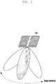
- FIG. 1 illustrates beam sweeping through a wireless communication chip according to an embodiment of the disclosure.
- a communication system that transmits and receives using mmWave band is fundamentally different from a wireless communication method.
- the gain loss of a beam emitted through an electronic device may increase.
- a multi-chain structure may be used to minimize the gain loss of a beam.
- an electronic device may include at least one wireless communication chip 100, and the at least one wireless communication chip 100 may generate four multi-chains.
- an electronic device including the wireless communication chip 100 may configure a beam using a multi-chain generated through the wireless communication chip 100, and may perform beam sweeping. That is, a multi-chain may refer to a plurality of radio frequency (RF) chains.
- RF radio frequency
- 16 or 32 multi-chains may be generated through one wireless communication chip 100.
- an electronic device may include four wireless communication chips, and each wireless communication chip included in the electronic device may generate 32 multi-chains.
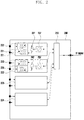
- FIG. 2 is a configuration diagram illustrating an electronic device including a multi-chain structure according to an embodiment of the disclosure.
- an electronic device 200 may include a plurality of antenna modules 221, 222, 223, and 224.
- a first antenna module 221 may include a first amplifier 231 configured to amplify a signal received from a communication circuit
- a second antenna module 222 may include a third amplifier 233 configured to amplify a signal received from the communication circuit.
- the signal received from the communication circuit may be an RF signal.
- a signal distributor 210 may transmit the RF signal received from the communication circuit to each of the antenna modules 221, 222, 223, and 224.
- each of the antenna modules 221, 222, 223, and 224 may configure a beam having a specific frequency band on the basis of an RF signal distributed from the signal distributor 210.
- the specific frequency band may be a frequency band used in a 5G mobile communication system.
- each of the antenna modules 221, 222, 223, 224 may configure a beam having a center frequency of 60 GHz, 39 GHz, or 28 GHz.
- the signal distributor 210 may operate as a signal combiner configured to combine RF signals received by each of the antenna modules 221, 222, 223, and 224.
- the first antenna module 221 may include a first phase shifter 251 configured to shift the phase of an RF signal distributed from the signal distributor 210, a first switch 241 configured to selectively connect a transmitting terminal and a receiving terminal, a first amplifier 231 connected to a transmitting terminal of the first antenna module 221 for amplifying power of an RF signal supplied from a communication circuit, and a second amplifier 232 connected to an output terminal of the first antenna module 221 for amplifying power of an RF signal supplied from outside the electronic device 200.
- a first phase shifter 251 configured to shift the phase of an RF signal distributed from the signal distributor 210
- a first switch 241 configured to selectively connect a transmitting terminal and a receiving terminal
- a first amplifier 231 connected to a transmitting terminal of the first antenna module 221 for amplifying power of an RF signal supplied from a communication circuit
- a second amplifier 232 connected to an output terminal of the first antenna module 221 for amplifying power of an RF signal supplied from outside the electronic device
- the first amplifier 231 may be a power amplifier (PA), and the second amplifier 232 may be a low-noise amplifier (LNA).
- the second amplifier 232 has a low noise figure (NF), and thus may generate low noise.
- the second antenna module 222 may include a second phase shifter 252 configured to shift the phase of an RF signal distributed from the signal distributor 210, a second switch 242 configured to selectively connect a transmitting terminal and a receiving terminal, a third amplifier 233 connected to a transmitting terminal of the second antenna module 222 and amplifying the power of an RF signal supplied from a communication circuit, and a fourth amplifier 234 connected to an output terminal of the second antenna module 222 and amplifying the power of an RF signal supplied from outside the electronic device 200.
- the third amplifier 233 may be a PA
- the fourth amplifier 234 may be a LNA.
- the fourth amplifier 234 has a low NF, and thus may generate low noise.
- the internal structures of the third antenna module 223 and the fourth antenna module 224 may also be the same as or similar to the internal structures of the first antenna module 221 and the second antenna module 222.
- each of the third antenna module 223 and the fourth antenna module 224 may also include a phase shifter, a switch, and a power amplifier corresponding thereto.
- the electronic device 200 may configure a first chain through the first antenna module 221, a second chain through the second antenna module 222, a third chain through the third antenna module 223, and a fourth chain through the fourth antenna module 224.
- the electronic device 200 may have a multi-chain structure including four chains, which includes the first antenna module 221, the second antenna module 222, the third antenna module 223, and the fourth antenna module 224.
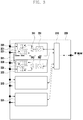
- FIG. 3 is a configuration diagram illustrating an electronic device including an impedance matching unit according to an embodiment of the disclosure.
- electronic device 300 includes a first antenna module 321 including a first amplifier 331 configured to amplify a signal received from a communication circuit, a second antenna module 322 including a third amplifier 333 configured to amplify the signal received from the communication circuit, and an impedance matching unit 361 disposed between an output terminal of the first amplifier 331 and an output terminal of the third amplifier 333.
- the impedance matching unit 361 may be a quarter-wave transformer ( ⁇ /4), and may combine output terminals of the first antenna module 321 and the second antenna module 322.
- the impedance matching unit 361 may be a passive device having a phase of ⁇ /4. For example, if the matching impedance of an output terminal of an electronic device 300 is 50 ⁇ , the characteristic impedance of ⁇ /4 may be 50 ⁇ .
- a signal distributor 310 may transmit an RF signal that is received from a communication circuit to each of antenna modules 321, 322, 323, and 324.
- each of the antenna modules 321, 322, 323, and 324 may configure a beam having a specific frequency band based on an RF signal distributed from the signal distributor 310.
- the specific frequency band may be a frequency band used in a 5G mobile communication system.
- each of the antenna modules 321, 322, 323, 324 may configure a beam having a center frequency of 60 GHz, 39 GHz, or 28 GHz.
- the signal distributor 310 may operate as a signal combiner configured to combine RF signals received by the respective antenna modules 321, 322, 323, and 324.
- the first antenna module 321 may include a first phase shifter 351 configured to shift a phase of an RF signal distributed from the signal distributor 310, a first switch 341 configured to selectively connect a transmitting terminal and a receiving terminal, and a second amplifier 332 connected to an output terminal of the first antenna module 321 and amplifying the power of an RF signal supplied from outside the electronic device 300.
- the first amplifier 331 may be a PA
- the second amplifier 332 may be a LNA.
- the second amplifier 332 has a low NF, and thus may generate low noise.
- the second antenna module 322 may include a second phase shifter 352 configured to shift the phase of an RF signal distributed from the signal distributor 310, a second switch 342 configured to selectively connect a transmitting terminal and a receiving terminal, a third amplifier 333 connected to a transmitting terminal of the second antenna module 322 and amplifying power of an RF signal supplied from a communication circuit, and a fourth amplifier 334 connected to an output terminal of the second antenna module 322 and amplifying the power of an RF signal supplied from outside the electronic device 300.
- a second phase shifter 352 configured to shift the phase of an RF signal distributed from the signal distributor 310
- a second switch 342 configured to selectively connect a transmitting terminal and a receiving terminal
- a third amplifier 333 connected to a transmitting terminal of the second antenna module 322 and amplifying power of an RF signal supplied from a communication circuit
- a fourth amplifier 334 connected to an output terminal of the second antenna module 322 and amplifying the power of an RF signal supplied from outside the
- the third amplifier 333 may be a PA
- the fourth amplifier 334 may be a LNA.
- the fourth amplifier 334 has a low NF, and thus may generate low noise.
- the phase of the RF signal shifted by the first phase shifter 351 and the phase of the RF signal shifted by the second phase shifter 352 may have a phase difference of 90 degrees therebetween.
- the first amplifier 331 and the third amplifier 333 may operate differently due to a phase difference between RF signals supplied to the first amplifier 331 and the third amplifier 333.
- the third amplifier 333 may operate as an amplifier at the time point at which the first amplifier 331 is saturated.
- the first antenna module 321, the second antenna module 322, and the impedance matching unit 361 may be arranged in a single chip.
- the first antenna module 321 and the second antenna module 322 may be built in a single integrated circuit (i.e., chip), and the impedance matching unit 361 may be integral or mounted to a package substrate that the single chip is also mounted to, which is molded using a resin to create a packaged integrated circuit.
- the impedance matching unit 361 may be implemented as a combination of a transmission line or a passive device in the package substrate.
- the impedance matching unit 361 shifts the phase of an output signal of the first amplifier 331 or the phase of an output signal of the third amplifier 333 by 90 degrees to combine the output signals of the first amplifier 331 and the third amplifier 333.
- a phase difference between an output RF signal of the first amplifier 331 and an output RF signal of the third amplifier 333, which is generated due to the first phase shifter 351, may be matched through the impedance matching unit 361.
- the internal structures of the third antenna module 323 and the fourth antenna module 324 may also be the same as or similar to the internal structures of the first antenna module 321 and the second antenna module 322.
- each of the third antenna module 323 and the fourth antenna module 324 may also include a phase shifter, a switch, and a power amplifier corresponding thereto.
- the electronic device 300 configures a first chain through the first antenna module 321, a second chain through the second antenna module 322, a third chain through the third antenna module 323, and a fourth chain through the fourth antenna module ray 324.
- the electronic device 300 may have a multi-chain structure including four chains, which includes the first antenna module 321, the second antenna module 322, the third antenna module 323, and the fourth antenna module 324.
- the first amplifier 331 included in the first antenna module 321 may operate as a carrier amplifier
- the third amplifier 333 included in the second antenna module 322 may operate as a peaking amplifier
- FIG. 4 illustrates a power amplification algorithm according to an embodiment of the disclosure.
- power amplification of the RF signal may be performed using a power distributor 410, a first phase shifter 421, a second phase shifter 422, a first amplifier 431, a second amplifier 432, an impedance matching unit 440, a first antenna 451, and a second antenna 452.
- the power distributor 410 may distribute to, a first phase shifter 421 and a second phase shifter 422, an RF signal supplied from a communication circuit.
- the number of chains of an electronic device including the power amplification algorithm may be determined on the basis of the number of RF signals distributed through the power distributor 410.
- the electronic device may include 16 multi-chain structures.
- the RF signal passing through the first phase shifter 421, the first amplifier 431, the impedance matching unit 440, and the first antenna 451 may configure a first chain.
- the RF signal passing through the second phase shifter 422, the second amplifier 432, and the second antenna 452 may configure a second chain.
- the first phase shifter 421 may shift a phase of the received RF signal as much as a first angle and transfer the shifted RF signal to the first amplifier 431.
- the second phase shifter 422 may shift a phase of the received RF signal as much as a second angle and transfer the shifted RF signal to the second amplifier 432.
- the first phase shifter 421 may shift the phase of the received RF signal as much as 120 degrees and transfer the shifted RF signal to the first amplifier 431
- the second phase shifter 422 may shift the phase of the received RF signal as much as 30 degrees and transfer the shifted RF signal to the second amplifier 432.
- the first amplifier 431 and the second amplifier 432 may amplify and output the power of the received RF signal.
- the first amplifier 431 may operate as a carrier amplifier
- the second amplifier 432 may operate as a peaking amplifier.
- an operating region of the first amplifier 431 and an operating region of the second amplifier 432 may be different from each other.
- the second amplifier 432 may perform power amplification in the case where the first amplifier 431 is saturated.
- the impedance matching unit 440 may have a quarter-wave transformer characteristic.
- the impedance matching unit 440 may compensate for a phase difference between an output signal of the first amplifier 431 and an output signal of the second amplifier 432, the phase difference occurring due to the first phase shifter 421 and the second phase shifter 422.
- FIG. 5 illustrates a graph of an efficiency comparison between an electronic device according to an embodiment of the disclosure and an electronic device according to the conventional art according to an embodiment of the disclosure.
- an antenna efficiency in the case where output power is P 1 is similar to an antenna efficiency in the case where the maximum output power is P 2 .
- P 1 may be a 6dB back-off parameter of P 2 the maximum output power.
- an antenna module may operate in a region where output power is lower than the maximum output power due to a high peak-to-average power ratio (PAPR) characteristic. Therefore, according to an antenna module structure disclosed in the disclosure, even if the operation output power of an antenna module is lowered, the high efficiency of the antenna module can be maintained.
- PAPR peak-to-average power ratio
- the disclosure provides an electronic device including: a first antenna module including a first amplifier configured to amplify a signal received from a communication circuit; a second antenna module including a second amplifier configured to amplify a signal received from the communication circuit; and an impedance matching unit disposed between an output terminal of the first amplifier and an output terminal of the second amplifier.
- the impedance matching unit may be a transmission line having a length of ⁇ /4.
- the impedance matching unit is a passive device having a phase of ⁇ /4.
- the first antenna module may include a first phase shifter connected to an input terminal of the first amplifier and shifting the phase of a signal received from the communication circuit
- the second antenna module may include a second phase shifter connected to an input terminal of the second amplifier and shifting the phase of a signal received from the communication circuit
- the phase difference between the phase shifted by the first phase shifter and the phase shifted by the second phase shifter may be 90 degrees.
- the second amplifier may operate in the case where the first amplifier is saturated.
- a first RF chain may be configured through the first antenna module
- a second RF chain may be configured through the second antenna module
- beam sweeping may be performed using the first antenna module and the second antenna module.
- the first antenna module, the second antenna module, and the impedance matching unit may be built in a chip.
- the first antenna module and the second antenna module may be built in a chip, and the impedance matching unit may be included in a packaging module including the chip.
- the impedance matching unit may shift the phase of an output signal of the first amplifier or the phase of an output signal of the second amplifier by 90 degrees so as to combine the output signal of the first amplifier and the output signal of the second amplifier.
- the disclosure may include: a first antenna module including a first amplifier configured to amplify a signal received from a communication circuit; a second antenna module including a second amplifier configured to amplify a signal received from the communication circuit; and an impedance matching unit disposed between an output terminal of the first amplifier and an output terminal of the second amplifier.
- the impedance matching unit may be a transmission line having a length of ⁇ /4.
- the impedance matching unit is a passive device having a phase of ⁇ /4.
- the first antenna module may include a first phase shifter connected to an input terminal of the first amplifier and shifting the phase of a signal received from the communication circuit
- the second antenna module may include a second phase shifter connected to an input terminal of the second amplifier and shifting the phase of a signal received from the communication circuit
- the phase difference between the phase shifted by the first phase shifter and the phase shifted by the second phase shifter may be 90 degrees.
- the second amplifier may operate in the case where the first amplifier is saturated.
- a first RF chain may be configured through the first antenna module
- a second RF chain may be configured through the second antenna module
- beam sweeping may be performed using the first antenna module and the second antenna module.
- the first antenna module, the second antenna array, and the impedance matching unit may be built in a chip.
- the first antenna module and the second antenna module may be built in a chip, and the impedance matching unit may be included in a packaging module including the chip.
- the impedance matching unit may shift the phase of an output signal of the first amplifier or the phase of an output signal of the second amplifier by 90 degrees so as to combine the output signal of the first amplifier and the output signal of the second amplifier.
Landscapes
- Engineering & Computer Science (AREA)
- Computer Networks & Wireless Communication (AREA)
- Signal Processing (AREA)
- Power Engineering (AREA)
- Variable-Direction Aerials And Aerial Arrays (AREA)
- Amplifiers (AREA)
- Transmitters (AREA)
Applications Claiming Priority (1)
| Application Number | Priority Date | Filing Date | Title |
|---|---|---|---|
| KR1020180168447A KR102581317B1 (ko) | 2018-12-24 | 2018-12-24 | 복수개의 안테나 어레이를 포함하는 전자 장치 |
Publications (2)
| Publication Number | Publication Date |
|---|---|
| EP3675381A2 true EP3675381A2 (fr) | 2020-07-01 |
| EP3675381A3 EP3675381A3 (fr) | 2020-07-08 |
Family
ID=69055674
Family Applications (1)
| Application Number | Title | Priority Date | Filing Date |
|---|---|---|---|
| EP19219545.1A Withdrawn EP3675381A3 (fr) | 2018-12-24 | 2019-12-23 | Dispositif électronique comprenant une pluralité de réseaux d'antennes |
Country Status (4)
| Country | Link |
|---|---|
| US (1) | US10897280B2 (fr) |
| EP (1) | EP3675381A3 (fr) |
| KR (1) | KR102581317B1 (fr) |
| CN (1) | CN111355518B (fr) |
Families Citing this family (2)
| Publication number | Priority date | Publication date | Assignee | Title |
|---|---|---|---|---|
| KR102725091B1 (ko) * | 2018-07-26 | 2024-11-04 | 삼성전자주식회사 | 무선 통신 시스템에서 송신 신호들을 증폭하기 위한 장치 및 방법 |
| US11962341B2 (en) * | 2020-12-24 | 2024-04-16 | Samsung Electronics Co., Ltd. | Electronic device and method for wireless communication |
Citations (1)
| Publication number | Priority date | Publication date | Assignee | Title |
|---|---|---|---|---|
| EP2741422B1 (fr) * | 2012-12-05 | 2015-07-01 | Nxp B.V. | Émetteur-récepteur multibande concurrent |
Family Cites Families (26)
| Publication number | Priority date | Publication date | Assignee | Title |
|---|---|---|---|---|
| US6472934B1 (en) | 2000-12-29 | 2002-10-29 | Ericsson Inc. | Triple class E Doherty amplifier topology for high efficiency signal transmitters |
| KR100480496B1 (ko) * | 2002-11-18 | 2005-04-07 | 학교법인 포항공과대학교 | 도허티 증폭기를 이용한 신호 증폭 장치 |
| US7512386B2 (en) * | 2003-08-29 | 2009-03-31 | Nokia Corporation | Method and apparatus providing integrated load matching using adaptive power amplifier compensation |
| FR2901929B1 (fr) * | 2006-05-31 | 2008-08-15 | St Microelectronics Sa | Dephaseur integre de signaux differentiels en signaux en quadrature |
| CN101523759A (zh) * | 2006-10-02 | 2009-09-02 | 施克莱无线公司 | 集中式无线通信系统 |
| KR100862056B1 (ko) * | 2007-08-06 | 2008-10-14 | (주) 와이팜 | 광대역 전력 증폭 장치 |
| KR100905202B1 (ko) * | 2007-09-03 | 2009-06-26 | 성균관대학교산학협력단 | 도허티 증폭기 |
| US8022768B1 (en) * | 2008-12-19 | 2011-09-20 | Nortel Networks Limited | Doherty amplifier and method for operation thereof |
| US9391650B2 (en) * | 2011-02-11 | 2016-07-12 | Qualcomm Incorporated | Front-end RF filters with embedded impedance transformation |
| US8749306B2 (en) * | 2011-03-16 | 2014-06-10 | Cree, Inc. | Enhanced Doherty amplifier |
| KR101767718B1 (ko) * | 2011-11-04 | 2017-08-11 | 스카이워크스 솔루션즈, 인코포레이티드 | 전력 증폭기들에 대한 장치 및 방법 |
| US9030255B2 (en) * | 2012-03-19 | 2015-05-12 | Auriga Measurement Systems, LLC | Linearization circuit and related techniques |
| US9071202B2 (en) * | 2013-10-18 | 2015-06-30 | Alcatel Lucent | Doherty amplifier with peak branch RF conditioning |
| EP2869463B1 (fr) * | 2013-10-31 | 2016-01-06 | Samba Holdco Netherlands B.V. | Structure d'amplificateur Doherty |
| JP2015109600A (ja) * | 2013-12-05 | 2015-06-11 | 三星電子株式会社Samsung Electronics Co.,Ltd. | 通信装置 |
| TWI672918B (zh) * | 2014-08-17 | 2019-09-21 | 美商西凱渥資訊處理科技公司 | 用於使用3g/4g線性路徑組合之2g放大之電路及方法 |
| KR20160028972A (ko) * | 2014-09-04 | 2016-03-14 | 한국전자통신연구원 | 부하 변조 기반 빔공간 mimo 전송 방법 및 장치 |
| JP6029728B2 (ja) * | 2014-10-31 | 2016-11-24 | スカイワークス ソリューションズ,インコーポレイテッドSkyworks Solutions,Inc. | 位相シフト部品を備えたダイバーシティ受信器フロントエンドシステム |
| US9831837B2 (en) * | 2014-11-05 | 2017-11-28 | Qualcomm Incorporated | Dynamic power divider circuits and methods |
| US9882538B2 (en) * | 2015-03-24 | 2018-01-30 | Skyworks Solutions, Inc. | Distributed output matching network for a radio frequency power amplifier module |
| JP2018056923A (ja) * | 2016-09-30 | 2018-04-05 | 株式会社村田製作所 | 送受信モジュール |
| US9866259B1 (en) | 2016-11-23 | 2018-01-09 | Infineon Technologies Ag | Transmitter/receiver module for millimeter wave 5G MIMO communication systems |
| US10620297B2 (en) | 2016-12-22 | 2020-04-14 | Apple Inc. | Radar methods and apparatus using in phased array communication systems |
| US10211785B2 (en) | 2016-12-29 | 2019-02-19 | Nxp Usa, Inc. | Doherty amplifiers with passive phase compensation circuits |
| KR102696312B1 (ko) * | 2017-01-06 | 2024-08-20 | 삼성전자 주식회사 | 전력 증폭 장치 및 이를 포함하는 단말 또는 기지국 |
| US10972055B2 (en) * | 2018-06-15 | 2021-04-06 | Skyworks Solutions, Inc. | Integrated doherty power amplifier |
-
2018
- 2018-12-24 KR KR1020180168447A patent/KR102581317B1/ko active Active
-
2019
- 2019-12-23 EP EP19219545.1A patent/EP3675381A3/fr not_active Withdrawn
- 2019-12-23 US US16/725,243 patent/US10897280B2/en not_active Expired - Fee Related
- 2019-12-24 CN CN201911343119.8A patent/CN111355518B/zh active Active
Patent Citations (1)
| Publication number | Priority date | Publication date | Assignee | Title |
|---|---|---|---|---|
| EP2741422B1 (fr) * | 2012-12-05 | 2015-07-01 | Nxp B.V. | Émetteur-récepteur multibande concurrent |
Also Published As
| Publication number | Publication date |
|---|---|
| CN111355518B (zh) | 2024-03-01 |
| EP3675381A3 (fr) | 2020-07-08 |
| KR20200079005A (ko) | 2020-07-02 |
| CN111355518A (zh) | 2020-06-30 |
| KR102581317B1 (ko) | 2023-09-22 |
| US20200204202A1 (en) | 2020-06-25 |
| US10897280B2 (en) | 2021-01-19 |
Similar Documents
| Publication | Publication Date | Title |
|---|---|---|
| KR102689200B1 (ko) | 안테나 모듈 및 안테나 모듈을 포함하는 전자 장치 | |
| US12051860B2 (en) | Antenna module including dielectric material and electronic device including antenna module | |
| KR102807427B1 (ko) | 통신 시스템에서의 기준 신호 전력 부스팅 | |
| US11362697B2 (en) | Multilayer printed circuit board and electronic device including the same | |
| US12009566B2 (en) | Four-way power divider and combiner for phased array system | |
| US11871516B2 (en) | Printed circuit board including coaxial plated through hole and electronic apparatus including same in wireless communication system | |
| US20230198161A1 (en) | Antenna module capable of supporting broadband and base station comprising same | |
| US10897280B2 (en) | Electronic device including plurality of antenna arrays | |
| US11211979B2 (en) | Method and apparatus for controlling transmission power in wireless communication system | |
| US11283532B2 (en) | Method for testing wireless communication module and electronic device including the wireless communication module | |
| CN113330647B (zh) | 包括用于减少向后波瓣辐射的无线电波的金属结构的天线模块和包括该天线模块的电子设备 | |
| EP3935796B1 (fr) | Procédé et appareil de détermination d'une fréquence locale dans un système de communication sans fil | |
| US11528081B2 (en) | Base station and control method therefor in wireless communication system | |
| US11165403B2 (en) | Antenna module using transmission line length and electronic device including the same | |
| CA3097520C (fr) | Module d'antenne comprenant un materiau dielectrique et dispositif electronique comprenant un module d'antenne |
Legal Events
| Date | Code | Title | Description |
|---|---|---|---|
| PUAI | Public reference made under article 153(3) epc to a published international application that has entered the european phase |
Free format text: ORIGINAL CODE: 0009012 |
|
| STAA | Information on the status of an ep patent application or granted ep patent |
Free format text: STATUS: THE APPLICATION HAS BEEN PUBLISHED |
|
| PUAL | Search report despatched |
Free format text: ORIGINAL CODE: 0009013 |
|
| AK | Designated contracting states |
Kind code of ref document: A2 Designated state(s): AL AT BE BG CH CY CZ DE DK EE ES FI FR GB GR HR HU IE IS IT LI LT LU LV MC MK MT NL NO PL PT RO RS SE SI SK SM TR |
|
| AX | Request for extension of the european patent |
Extension state: BA ME |
|
| AK | Designated contracting states |
Kind code of ref document: A3 Designated state(s): AL AT BE BG CH CY CZ DE DK EE ES FI FR GB GR HR HU IE IS IT LI LT LU LV MC MK MT NL NO PL PT RO RS SE SI SK SM TR |
|
| AX | Request for extension of the european patent |
Extension state: BA ME |
|
| RIC1 | Information provided on ipc code assigned before grant |
Ipc: H01Q 1/52 20060101ALI20200604BHEP Ipc: H04B 7/06 20060101AFI20200604BHEP Ipc: H01Q 3/26 20060101ALI20200604BHEP |
|
| STAA | Information on the status of an ep patent application or granted ep patent |
Free format text: STATUS: REQUEST FOR EXAMINATION WAS MADE |
|
| 17P | Request for examination filed |
Effective date: 20201001 |
|
| RBV | Designated contracting states (corrected) |
Designated state(s): AL AT BE BG CH CY CZ DE DK EE ES FI FR GB GR HR HU IE IS IT LI LT LU LV MC MK MT NL NO PL PT RO RS SE SI SK SM TR |
|
| STAA | Information on the status of an ep patent application or granted ep patent |
Free format text: STATUS: EXAMINATION IS IN PROGRESS |
|
| 17Q | First examination report despatched |
Effective date: 20210428 |
|
| STAA | Information on the status of an ep patent application or granted ep patent |
Free format text: STATUS: THE APPLICATION IS DEEMED TO BE WITHDRAWN |
|
| 18D | Application deemed to be withdrawn |
Effective date: 20250701 |