EP3675603B1 - Circuit de commande et procédé de commande de charge de diode électroluminescente - Google Patents
Circuit de commande et procédé de commande de charge de diode électroluminescente Download PDFInfo
- Publication number
- EP3675603B1 EP3675603B1 EP19219127.8A EP19219127A EP3675603B1 EP 3675603 B1 EP3675603 B1 EP 3675603B1 EP 19219127 A EP19219127 A EP 19219127A EP 3675603 B1 EP3675603 B1 EP 3675603B1
- Authority
- EP
- European Patent Office
- Prior art keywords
- current
- driving
- voltage
- led load
- power transistor
- Prior art date
- Legal status (The legal status is an assumption and is not a legal conclusion. Google has not performed a legal analysis and makes no representation as to the accuracy of the status listed.)
- Active
Links
Images




Classifications
-
- H—ELECTRICITY
- H05—ELECTRIC TECHNIQUES NOT OTHERWISE PROVIDED FOR
- H05B—ELECTRIC HEATING; ELECTRIC LIGHT SOURCES NOT OTHERWISE PROVIDED FOR; CIRCUIT ARRANGEMENTS FOR ELECTRIC LIGHT SOURCES, IN GENERAL
- H05B45/00—Circuit arrangements for operating light-emitting diodes [LED]
- H05B45/30—Driver circuits
- H05B45/37—Converter circuits
- H05B45/3725—Switched mode power supply [SMPS]
-
- H—ELECTRICITY
- H05—ELECTRIC TECHNIQUES NOT OTHERWISE PROVIDED FOR
- H05B—ELECTRIC HEATING; ELECTRIC LIGHT SOURCES NOT OTHERWISE PROVIDED FOR; CIRCUIT ARRANGEMENTS FOR ELECTRIC LIGHT SOURCES, IN GENERAL
- H05B45/00—Circuit arrangements for operating light-emitting diodes [LED]
- H05B45/40—Details of LED load circuits
- H05B45/44—Details of LED load circuits with an active control inside an LED matrix
-
- H—ELECTRICITY
- H02—GENERATION; CONVERSION OR DISTRIBUTION OF ELECTRIC POWER
- H02M—APPARATUS FOR CONVERSION BETWEEN AC AND AC, BETWEEN AC AND DC, OR BETWEEN DC AND DC, AND FOR USE WITH MAINS OR SIMILAR POWER SUPPLY SYSTEMS; CONVERSION OF DC OR AC INPUT POWER INTO SURGE OUTPUT POWER; CONTROL OR REGULATION THEREOF
- H02M1/00—Details of apparatus for conversion
- H02M1/08—Circuits specially adapted for the generation of control voltages for semiconductor devices incorporated in static converters
-
- H—ELECTRICITY
- H05—ELECTRIC TECHNIQUES NOT OTHERWISE PROVIDED FOR
- H05B—ELECTRIC HEATING; ELECTRIC LIGHT SOURCES NOT OTHERWISE PROVIDED FOR; CIRCUIT ARRANGEMENTS FOR ELECTRIC LIGHT SOURCES, IN GENERAL
- H05B45/00—Circuit arrangements for operating light-emitting diodes [LED]
- H05B45/10—Controlling the intensity of the light
-
- H—ELECTRICITY
- H05—ELECTRIC TECHNIQUES NOT OTHERWISE PROVIDED FOR
- H05B—ELECTRIC HEATING; ELECTRIC LIGHT SOURCES NOT OTHERWISE PROVIDED FOR; CIRCUIT ARRANGEMENTS FOR ELECTRIC LIGHT SOURCES, IN GENERAL
- H05B45/00—Circuit arrangements for operating light-emitting diodes [LED]
- H05B45/40—Details of LED load circuits
- H05B45/44—Details of LED load circuits with an active control inside an LED matrix
- H05B45/46—Details of LED load circuits with an active control inside an LED matrix having LEDs disposed in parallel lines
-
- H—ELECTRICITY
- H02—GENERATION; CONVERSION OR DISTRIBUTION OF ELECTRIC POWER
- H02M—APPARATUS FOR CONVERSION BETWEEN AC AND AC, BETWEEN AC AND DC, OR BETWEEN DC AND DC, AND FOR USE WITH MAINS OR SIMILAR POWER SUPPLY SYSTEMS; CONVERSION OF DC OR AC INPUT POWER INTO SURGE OUTPUT POWER; CONTROL OR REGULATION THEREOF
- H02M1/00—Details of apparatus for conversion
- H02M1/0048—Circuits or arrangements for reducing losses
- H02M1/0054—Transistor switching losses
-
- H—ELECTRICITY
- H05—ELECTRIC TECHNIQUES NOT OTHERWISE PROVIDED FOR
- H05B—ELECTRIC HEATING; ELECTRIC LIGHT SOURCES NOT OTHERWISE PROVIDED FOR; CIRCUIT ARRANGEMENTS FOR ELECTRIC LIGHT SOURCES, IN GENERAL
- H05B45/00—Circuit arrangements for operating light-emitting diodes [LED]
- H05B45/10—Controlling the intensity of the light
- H05B45/14—Controlling the intensity of the light using electrical feedback from LEDs or from LED modules
-
- H—ELECTRICITY
- H05—ELECTRIC TECHNIQUES NOT OTHERWISE PROVIDED FOR
- H05B—ELECTRIC HEATING; ELECTRIC LIGHT SOURCES NOT OTHERWISE PROVIDED FOR; CIRCUIT ARRANGEMENTS FOR ELECTRIC LIGHT SOURCES, IN GENERAL
- H05B45/00—Circuit arrangements for operating light-emitting diodes [LED]
- H05B45/30—Driver circuits
-
- H—ELECTRICITY
- H05—ELECTRIC TECHNIQUES NOT OTHERWISE PROVIDED FOR
- H05B—ELECTRIC HEATING; ELECTRIC LIGHT SOURCES NOT OTHERWISE PROVIDED FOR; CIRCUIT ARRANGEMENTS FOR ELECTRIC LIGHT SOURCES, IN GENERAL
- H05B47/00—Circuit arrangements for operating light sources in general, i.e. where the type of light source is not relevant
- H05B47/10—Controlling the light source
-
- H—ELECTRICITY
- H05—ELECTRIC TECHNIQUES NOT OTHERWISE PROVIDED FOR
- H05B—ELECTRIC HEATING; ELECTRIC LIGHT SOURCES NOT OTHERWISE PROVIDED FOR; CIRCUIT ARRANGEMENTS FOR ELECTRIC LIGHT SOURCES, IN GENERAL
- H05B47/00—Circuit arrangements for operating light sources in general, i.e. where the type of light source is not relevant
- H05B47/10—Controlling the light source
- H05B47/105—Controlling the light source in response to determined parameters
- H05B47/14—Controlling the light source in response to determined parameters by determining electrical parameters of the light source
-
- H—ELECTRICITY
- H05—ELECTRIC TECHNIQUES NOT OTHERWISE PROVIDED FOR
- H05B—ELECTRIC HEATING; ELECTRIC LIGHT SOURCES NOT OTHERWISE PROVIDED FOR; CIRCUIT ARRANGEMENTS FOR ELECTRIC LIGHT SOURCES, IN GENERAL
- H05B47/00—Circuit arrangements for operating light sources in general, i.e. where the type of light source is not relevant
- H05B47/10—Controlling the light source
- H05B47/16—Controlling the light source by timing means
-
- Y—GENERAL TAGGING OF NEW TECHNOLOGICAL DEVELOPMENTS; GENERAL TAGGING OF CROSS-SECTIONAL TECHNOLOGIES SPANNING OVER SEVERAL SECTIONS OF THE IPC; TECHNICAL SUBJECTS COVERED BY FORMER USPC CROSS-REFERENCE ART COLLECTIONS [XRACs] AND DIGESTS
- Y02—TECHNOLOGIES OR APPLICATIONS FOR MITIGATION OR ADAPTATION AGAINST CLIMATE CHANGE
- Y02B—CLIMATE CHANGE MITIGATION TECHNOLOGIES RELATED TO BUILDINGS, e.g. HOUSING, HOUSE APPLIANCES OR RELATED END-USER APPLICATIONS
- Y02B20/00—Energy efficient lighting technologies, e.g. halogen lamps or gas discharge lamps
- Y02B20/40—Control techniques providing energy savings, e.g. smart controller or presence detection
-
- Y—GENERAL TAGGING OF NEW TECHNOLOGICAL DEVELOPMENTS; GENERAL TAGGING OF CROSS-SECTIONAL TECHNOLOGIES SPANNING OVER SEVERAL SECTIONS OF THE IPC; TECHNICAL SUBJECTS COVERED BY FORMER USPC CROSS-REFERENCE ART COLLECTIONS [XRACs] AND DIGESTS
- Y02—TECHNOLOGIES OR APPLICATIONS FOR MITIGATION OR ADAPTATION AGAINST CLIMATE CHANGE
- Y02B—CLIMATE CHANGE MITIGATION TECHNOLOGIES RELATED TO BUILDINGS, e.g. HOUSING, HOUSE APPLIANCES OR RELATED END-USER APPLICATIONS
- Y02B70/00—Technologies for an efficient end-user side electric power management and consumption
- Y02B70/10—Technologies improving the efficiency by using switched-mode power supplies [SMPS], i.e. efficient power electronics conversion e.g. power factor correction or reduction of losses in power supplies or efficient standby modes
Definitions
- the present disclosure relates to the technical field of power electronics, and in particular to a driving circuit and a driving method for driving a light emitting diode (LED) loac
- the invention relates to a driving circuit for driving a light emitting diode according to claim 1 and a method for driving a light emitting diode according to claim 10.
- Preferred embodiments of the invention are defined by the dependent claims.
- LEDs Light emitting diodes
- LED driving methods include a linear driving method and a switching driving method.
- a switching converter is used to control the constant current output to drive the LED load.
- the switching converter must include at least a main power transistor, a rectifier tube, and a magnetic element such as an inductor or a transformer, which results in a high circuit cost and complicated control.
- a driving current flowing through the LED load may be controlled to be constant only by linear control for a power transistor.
- FIG. 1 is a functional block diagram of an LED driving circuit in the conventional technology, in which the linear driving method is used to provide the driving current for the LED load.
- the LED driving circuit is connected to an output end of a rectifier bridge BR to receive a direct current bus voltage VBUS.
- a filter capacitor may be connected to the output end of the rectifier bridge BR.
- the LED driving circuit includes: a sampling resistor Rs and a power transistor Qs that are connected in series with the LED load, and an output capacitor Co that is connected in parallel with the LED load , and a constant current control circuit.
- the constant current control circuit includes at least an averaging circuit 11, a compensation circuit 12, and a drive signal generating circuit 13.
- the sampling resistor Rs is used to sample a current flowing through the LED load.
- the averaging circuit 11 is used to convert a sampling signal across the sampling resistor Rs into a current detection signal representing an average current flowing through the LED load. The average current corresponds to a brightness of the LED load.
- the compensation circuit 12 is used to calculate an error between the current detection signal and a reference current signal corresponding to a desired brightness of the LED load and perform an error compensation operation to generate a compensation signal Vcomp representing an error between a current average current and the desired current.
- the drive signal generating circuit 13 is used to generate a drive signal based on the compensation signal Vcomp to drive a control terminal of the power transistor Qs, so as to adjust the current flowing through the LED load.
- the drive signal is increased by the closed-loop feedback control to increase the current flowing through the power transistor, so that the average current is increased and is maintained at the desired current.
- the drive signal is decreased by the closed-loop feedback control to decrease the current flowing through the power transistor, so that the average current is decreased and is maintained at the desired current.
- US 2018/310376 A1 discloses a method of constant current control for the LED load.
- the LED driver can include silicon-controlled dimmer TRIAC, a rectifier circuit, constant current control circuit CON, and bleed resistor R1.
- Constant current control circuit CON can integrate an LED load and regulate a load current flowing through the LED load through transistor Q.
- load current sampling signal Ref1 can be sampled by resistor R2 coupled in series with transistor Q and fed back to error amplifier EA. Error amplifier Ea can achieve constant current control for transistor Q according to load current reference signal Ref1 and load current sampling signal Ref1.
- the linear driving method in the conventional technology is implemented by the closed-loop feedback control.
- the constant current control circuit adjusts the drive signal based on the error between the current average current and the desired current to change the real-time current.
- the average current is maintained at the desired current by the closed-loop adjustment, so that the LED load has the desired brightness.
- the real-time current flowing through the LED load is provided by a power transistor and is substantially fixed in a certain time period. That is, the real-time current is substantially fixed in a time period in which the direct current bus voltage VBUS is higher than the voltage across the LED load. In a case that the direct current bus voltage VBUS is much higher than the voltage across the LED load, the loss of the power transistor is large, greatly reducing the operating efficiency of the LED driving circuit.
- a linear driving circuit and a linear driving method for driving an LED load according to embodiments of the present disclosure, to solve a problem of complicated linear control in the conventional technology.
- a driving method for driving an LED load includes:
- the transistor current in a first time period is controlled to be less than the transistor current in a second time period, where the difference between the input voltage and the driving voltage in the first time period is greater than the difference between the input voltage and the driving voltage in the second time period.
- a voltage threshold corresponding to the difference between the input voltage and the driving voltage is set.
- the transistor current in a first time period in which the difference between the input voltage and the driving voltage is greater than the voltage threshold is controlled to be less than the transistor current in a second time period in which the difference between the input voltage and the driving voltage is less than the voltage threshold.
- reference currents according to the predetermined requirement are set.
- the transistor current is controlled to switch between the reference currents based on a comparison between the voltage threshold and the difference between the input voltage and the driving voltage.
- the transistor current is controlled to vary from one value to another value in a stepwise manner.
- the transistor current is controlled to be symmetrical with the transistor current during the half cycle in which the input voltage is in the rising phase.
- a time length that the transistor current switches from one value to another value is extended to improve an electro magnetic compatibility (EMC) performance.
- EMC electro magnetic compatibility
- the transistor current is controlled to vary from the one value to the another value in a ramp manner.
- the transistor current when a duration during which the transistor current is maintained at a first current reaches a first time threshold, the transistor current is controlled to switch to a second current, where the first current is greater than the second current.
- a duration during which the transistor current is maintained at the second current is detected.
- the transistor current is controlled to switch to the first current.
- the transistor current in the time period in which the input voltage is higher than the driving voltage, is controlled to switch between a first current and a second current, where the first current is greater than the second current. Based on a comparison between a voltage threshold and the difference between the input voltage and the driving voltage, durations of the first current and the second current are adjusted, so that the average current meets a requirement for driving the LED load in a case that the input voltage varies.
- the voltage threshold and a ratio of the first current to the second current are set, so that an error of the average current caused by variations of the durations of the first current and the second current is in a predetermined range, where the variations of the durations of the first current and the second current are caused by a variation of the input voltage and/or a variation of the driving voltage.
- the voltage threshold and the ratio of the first current to the second current are set based on the input voltage and a variation range of the driving voltage, so that the error of the average current caused by the variations of the durations of the first current and the second current is in the predetermined range, with the variations of the durations of the first current and the second current being caused by the variation of the driving voltage; or
- a driving circuit for driving an LED load includes: a power transistor and a control circuit, where
- control circuit includes a drive signal generating circuit.
- the drive signal generating circuit is configured to generate a drive signal based on the difference between the input voltage and the driving voltage, to control the power transistor so that the transistor current in in a first time period is controlled to be less than the transistor current in a second time period, where the difference between the input voltage and the driving voltage in the first time period is greater than the difference between the input voltage and the driving voltage in the second time period.
- control circuit includes a selecting circuit.
- the selecting circuit is configured to: select one of reference signals representing desired values of the transistor current based on the difference between the input voltage and the driving voltage, and deliver the selected reference signal to the drive signal generating circuit.
- the driving circuit further includes a first detecting circuit connected in series with the power transistor.
- the first detecting circuit is configured to detect an instantaneous current flowing through the power transistor and generate a current detection signal based on the detected instantaneous current.
- the drive signal generating circuit is configured to generate the drive signal based on the current detection signal and the selected reference signal, to drive a control terminal of the power transistor, so that the transistor current coincides with the selected reference signal.
- the selecting circuit includes switches and a logic circuit.
- the switches are arranged in one-to-one correspondence with the reference signals.
- the logic circuit is configured to generate control signals for controlling switching states of the switches based on the difference between the input voltage and the driving voltage.
- the driving circuit further includes a buffer circuit.
- the buffer circuit is coupled between the selecting circuit and the drive signal generating circuit, and is configured to extend a time length used for switching between the reference signals.
- the buffer circuit includes a filter circuit.
- the filter circuit is configured to filter a voltage signal the selected reference signal, so that the transistor current switches from one value to another value in a ramp manner.
- control circuit includes a timing circuit.
- the timing circuit is configured to control a maximum time length of a duration during which the transistor current is maintained at a current.
- control circuit is configured to control the transistor current to vary from one value to another value in a stepwise manner during a half cycle in which the input voltage is in a rising phase.
- control circuit is configured to control the transistor current during a half cycle in which the input voltage is in a falling phase to be symmetrical with the transistor current during the half cycle in which the input voltage is in the rising phase.
- the drive signal generating circuit is configured to: in the time period in which the input voltage is higher than the driving voltage, control the transistor current to be switched between a first current and a second current by using the drive signal, where the first current is greater than the second current; and adjust durations of the first current and the second current based on a comparison between a voltage threshold and the difference between the input voltage and the driving voltage, so that the average current meets a requirement for driving the LED load in a case that the input voltage varies.
- the drive signal generating circuit is configured to: in a cycle, in the case that the input voltage is higher than the driving voltage,
- control circuit is configured to: set the voltage threshold and a ratio of the first current to the second current based on the input voltage and the driving voltage, so that an error of the average current caused by variations of the durations of the first current and the second current is in a predetermined range, where the variations of the durations of the first current and the second current are caused by a variation of the input voltage and/or a variation of the driving voltage.
- control circuit is configured to:
- control circuit includes a timing circuit.
- the timing circuit is configured to: when the duration of the first current reaches a time length represented by a first time threshold, control the transistor current to switch from the first current to the second current.
- the timing circuit is configured to: after the transistor current switches from the first current to the second current, when the duration of the second current reaches a time length represented by a second time threshold, control the transistor current to switch from the second current to the first current.
- the power transistor is controlled by the open-loop control in the driving method and the driving circuit for driving an LED load according to the embodiments of the present disclosure.
- the current of the power transistor is controlled based on the difference between the input voltage and the driving voltage, without calculating the error between the current average current of the LED load and the desired current by a closed-loop circuit. That is, the real-time current flowing through the LED load is controlled to be not fixed but vary with the difference between the input voltage and the driving voltage, to reduce the conduction loss of the power transistor.
- the durations of the currents of different values are adjusted, so that the average current flowing through the LED load can meet the requirement for driving the LED load to emit a light having a desired brightness, and a good output current adjustment rate can be obtained in the process that the input voltage varies.
- a “circuit” indicates a conductive loop formed by at least one component or sub-circuit by electrical connection or electromagnetic connection.
- a component or circuit is described as being “connected to” another component or being “connected” between two terminals, the component or circuit may be coupled or connected to another component directly or via an intermediate component.
- the connection between the two components may be physical connection, logical connection, or a combination thereof.
- the component is described as being “directly coupled to” or “directly connected to” another component, it is indicated that no intermediate component exists between the two components.
- Figure 2A is a flowchart of a driving method for driving an LED load according to a first embodiment of the present disclosure.
- the driving method for driving an LED load includes the following steps S21 to S22.
- a power transistor connected in series with the LED load is controlled to operate in a linear mode.
- the power transistor is connected in series with the LED load to form a current path, and is used to receive the input voltage varying periodically from an input end.
- the input voltage may be a sinusoidal half-wave input voltage.
- An alternating current input voltage may be rectified by a rectifying circuit to form the sinusoidal half-wave input voltage.
- a transistor current flowing through the power transistor is controlled based on a difference between the input voltage and the driving voltage, without calculating an error between an average current flowing through the LED load and a desired current.
- the current flowing through the power transistor is decreased, to reduce a conduction loss of the power transistor, and cause the average current flowing through the LED load to meet a predetermined requirement for driving the LED load to emit a light having a desired brightness.
- the transistor current generated by the power transistor is controlled based on the difference between the input voltage and the driving voltage, so that the transistor current in a time period in which the difference between the input voltage and the driving voltage is large is less than the transistor current in a time period in which the difference between the input voltage and the driving voltage is small.
- the transistor current is decreased as the difference between the input voltage and the driving voltage increases, to reduce the conduction loss of the power transistor.
- the difference between the input voltage and the driving voltage may be represented by a preset voltage threshold.
- Voltage thresholds with different values increasing sequentially may be set according to an actual control requirement, and a threshold interval is formed between two adjacent voltage thresholds.
- a reference current for the transistor current may be set correspondingly, to meet a requirement that the transistor current is decreased as the difference between the input voltage and the driving voltage increases.
- the transistor current is controlled to be a reference current corresponding to the threshold interval.
- the transistor current is controlled to be decreased stepwise.
- the transistor current is controlled to be symmetrical with the transistor current during the half cycle in which the input voltage is in the rising phase.
- the real-time current flowing through the power transistor may have multiple different values depending on the difference between the input voltage and the driving voltage.
- the current flowing through the power transistor may be controlled to be small if the difference between the input voltage and the driving voltage is large, and the current flowing through the power transistor may be controlled to be large if the difference between the input voltage and the driving voltage is small, reducing the conduction loss of the power transistor, while causing the average current flowing through the LED load to meet the requirement for driving the LED load to emit a light having a desired brightness.
- the specific operational process is described below by taking a case that the real-time current flowing through the LED load includes a first current with a large value and a second current with a small value as an example.
- a magnitude of the difference between the input voltage and the driving voltage may be represented by a comparison between the difference and a preset voltage threshold.
- a length of a time period in which the current flowing through the power transistor is the first current is controlled to not exceed a length of a time period in which the difference between the input voltage and the driving voltage is less than the preset voltage threshold.
- a length of a time period in which the current flowing through the power transistor is the second current is controlled to not exceed a length of a time period in which the difference between the input voltage and the driving voltage is greater than the preset voltage threshold.
- a voltage across the power transistor is approximately equal to the difference between the input voltage and the driving voltage. In the case that the voltage across the power transistor is large, the current flowing through the power transistor is the second current with a small value, so that the conduction loss of the power transistor is greatly reduced.
- the current flowing through the power transistor may also be the first current with a large value.
- the value of the first current is large, the voltage across the power transistor in the time period in which the current flowing through the power transistor is the first current is small. In this case, the conduction loss is relatively low.
- the average current of the first current with a large value and the second current with a small value in one cycle can meet the requirement for driving the LED load to emit a light having a desired brightness.
- FIG. 2B is an operational waveform diagram of the driving method for driving an LED load according to the first embodiment of the present disclosure shown in Figure 2A .
- VT represents the voltage across the power transistor
- Vth represents the set voltage threshold
- IQ represents the current flowing through the power transistor
- IREF 1 represents the first current with a large value that is preset
- IREF2 represents the second current with a small value that is preset.
- the voltage across the power transistor may be approximately equal to the difference between the input voltage VBUS and the driving voltage VLED.
- the driving voltage VLED may be considered as a fixed value. In this case, after the power transistor is turned on, that is, after the input voltage VBUS is higher than the driving voltage VLED, the voltage VT varies with the input voltage VBUS.
- the voltage threshold Vth is set to be a fixed value.
- the input voltage VBUS is a first sinusoidal half-wave voltage having a small effective value
- a voltage VT2 starts increasing from zero and varies with the input voltage VBUS.
- the voltage VT2 is lower than the voltage threshold Vth, which indicates that the voltage across the power transistor is small, and the current IQ in the time period from the time instant t1 to the time instant t3 may be the first current IREF 1 with a large value, to prevent excessive conduction power loss.
- the voltage VT2 In a time period from the time instant t3 to a time instant t4, the voltage VT2 is higher than the voltage threshold Vth, which indicates that the voltage across the power transistor is large, and the current IQ in the time period from the time instant t3 to the time instant t4 may be the second current IREF2 with a small value, to prevent excessive conduction power loss.
- the voltage VT2 in a falling phase of the voltage VT2, in a time period from the time instant t4 to a time instant t6, the voltage VT2 is lower than the voltage threshold Vth again, which indicates that the voltage across the power transistor is small, and the current IQ may be the first current IREF1 with a large value.
- a voltage VT1 starts increasing from zero at a time instant t0 and varies with the input voltage VBUS.
- the voltage VT1 is lower than the voltage threshold Vth, which indicates that the voltage across the power transistor is small, and the current IQ in the time period from the time period t0 to the time instant t2 may be the first current IREF 1 with a large value, to prevent excessive conduction power loss.
- the voltage VT1 is higher than the voltage threshold Vth, which indicates that the voltage across the power transistor is large, and the current IQ in the time period from the time instant t2 to the time instant t5 may be the second current IREF2 with a small value, to prevent excessive conduction power loss.
- the voltage VT1 in a time period from the time instant t5 to a time instant t7, the voltage VT1 is lower than the voltage threshold Vth again, which indicates that the voltage across the power transistor is small, and the current IQ in the time period from the time instant t5 to the time instant t7 may be the first current IREF1 with a large value.
- the average current flowing through the LED load corresponding to the brightness of the LED load is an average current in a cycle.
- an average current Iavg1 2 * t3 ⁇ t1 * IREF1 + t4 ⁇ t3 * IREF2 / Ts
- an average current Iavg2 is expressed by the following formula (2).
- Iavg2 2 * t2 ⁇ t0 * IREF1 + t5 ⁇ t2 * IREF2 / Ts
- Ts represents a power frequency cycle of the alternating current voltage
- Iavg1 and Iavg2 respectively represent averages of the first current and the second current in one power frequency cycle. It can be seen from the above formula (1) and formula (2) that, the duration (t3-t1) is greater than the duration (t2-t0), and the duration (t4-t3) is less than the duration (t5-t2).
- an appropriate voltage threshold Vth and a ratio of the first current to the second current are set, so that the variation of the average current caused by the variation of the input voltage VBUS is limited in a small range, for example, 5%.
- the small variation range meets the predetermined requirement for driving the LED load to emit a light having a desired brightness.
- a light source may be implemented by different LED loads.
- the number of LED strings may vary, so that the driving voltage for the LED load varies.
- the difference between the input voltage and the driving voltage for the LED load i.e., the voltage VT across the power transistor, varies with the driving voltage VLED. If the driving voltage increases, the voltage VT is decreases. If the driving voltage decreases, the voltage VT increases. Durations of the first current and the second current vary accordingly.
- the voltage threshold and the ratio of the first current to the second current are set based on the input voltage and the variation range of the driving voltage, so that the error of the average current is still controlled in a small range, for example, 5%, although the durations of the first current and the second current may vary due to the variation of the driving voltage.
- the small variation range meets the predetermined requirement for driving the LED load to emit a light having a desired brightness.
- the voltage threshold and the ratio of the first current to the second current are set based on the variation range of the input voltage and the variation range of the driving voltage, so that the errors of the average currents of the first current and the second current are controlled in a small range, for example, 5%.
- the small variation range meets the predetermined requirement for driving the LED load to emit a light having a desired brightness.
- the power transistor is controlled by the open-loop control in the driving method for driving an LED load according to the embodiments of the present disclosure.
- the current of the power transistor is controlled based on the difference between the input voltage and the driving voltage, without calculating the error between the current average current of the LED load and the desired current by a closed-loop circuit. That is, the real-time current flowing through the LED load is controlled to be not fixed but vary with the difference between the input voltage and the driving voltage, to reduce the conduction loss of the power transistor.
- the durations of the currents of different values are adjusted, so that the average current flowing through the LED load can meet the requirement for driving the LED load to emit a light having a desired brightness, and a good output current adjustment rate can be obtained in the process that the input voltage varies.
- a driving method for driving an LED load is further provided according to a second embodiment of the present disclosure.
- the driving method for driving an LED load according to the second embodiment may further include a step of extending a time length used for the transistor current switching between different current values, to obtain a good EMC performance.
- the transistor current is increased or decreased from a current value to another current value in a ramp manner, rather than stepwise varying between two different current values.
- Figure 3 is an operational waveform diagram of the driving method for driving an LED load according to the second embodiment. The following description is given by still taking the case that the real-time current flowing through the LED load includes a first current with a large value and a second current with a small value as an example.
- the input voltage VBUS is higher than the driving voltage VLED for the LED load, and the power transistor is turned on to allow a current to flow through the LED load.
- the difference between the input voltage VBUS and the driving voltage VLED is smaller than the voltage threshold Vth, which indicates that the voltage across the power transistor is small, and the current IQ in the time period from the time instant t0 to the time instant t1 may be the first current IREF1 with a large value, to prevent excessive conduction power loss.
- the difference between the input voltage VBUS and the driving voltage VLED starts to be greater than the voltage threshold Vth, and the current IQ is required to switch to the second current IREF2 with a small value from the first current IREF1.
- a time length used for the current IQ switching from the first current to the second current is extended, and the current IQ is slowly decreased to the second current from the first current.
- the current may be decreased to the second current from the first current at a certain decreasing slope.
- the difference between the input voltage VBUS and the driving voltage VLED starts to be less than the voltage threshold Vth, and the current IQ is required to switch to the first current with a large value from the second current.
- a time length used for the current IQ switching from the second current IREF2 to the first current IREF1 is extended, and the current IQ is slowly increased to the first current IREF1 from the second current IREF2.
- the current may be increased to the first current IREF1 from the second current IREF2 at a certain increasing slope. In this way, the current varies slowly, and the EMC performance is greatly improved.
- the input voltage VBUS starts to be higher than the driving voltage VLED, and the current IQ starts to switch from zero to the first current IREF 1.
- the time length used for the current switching from zero to the first current IREF 1 may be extended, and the current is slowly increased to the first current from zero.
- the input voltage VBUS starts to be lower than the driving voltage VLED for the LED load, and the current IQ starts to switch to zero from the first current.
- the time length used for the current switching from the first current to zero may be extended, and the current is slowly decreased to zero from the first current. In this way, the EMC performance of the circuit is further improved.
- a driving method for driving an LED load is further provided according to a third embodiment of the present disclosure.
- the driving method for driving an LED load according to the third embodiment may further include steps of controlling the duration of the current with a large value, to better ensure the normal driving for the LED load without being affected by the variation of the input voltage and other factors such as a dimming angle.
- the controlling process may be performed by: timing a duration during which the current flowing through the power transistor is the first current with a large value; and controlling the current flowing through the power transistor to switch from the first current to the second current with a small value when the duration during which the current flowing through the power transistor is the first current reaches a first time threshold.
- the duration during which the voltage across the power transistor is lower than the voltage threshold is relative long.
- a maximum time length of the duration of the current with a large value is limited with the driving method in this embodiment, avoiding the case that the requirement for driving the LED load to emit a light having a desired brightness is not met due to an excessively high average current.
- the driving method further includes: controlling the current flowing through the power transistor to switch to the second current from the first current when a first duration during which the current flowing through the power transistor is the first current reaches a first time threshold; timing the duration during which the current flowing through the power transistor is the second current; and controlling the current flowing through the power transistor to switch to the first current from the second current when the time length of the duration during which the current flowing through the power transistor is the second current reaches a second time threshold.
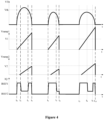
- Figure 4 is an operational waveform diagram of the driving method for driving an LED load according to the third embodiment. The following description is given by still taking the case that the real-time current flowing through the LED load includes a first current with a large value and a second current with a small value as an example.
- a length of the durations [t0-t1] and [t2-t3] of the first current IREF1 is less than a first time threshold
- a length of the duration of the second current IREF2 is a length of a time period from a time instant t1 to a time instant t2 in which the voltage VT is higher than the voltage threshold Vth.
- a length of the duration [t4-t5] of the first current IREF1 is limited to a time length represented by the first time threshold.
- the transistor current is maintained as the second current IREF2.
- a length of the duration [t7-t8] of the first current IREF1 is limited to the time length represented by the first time threshold. After the time length represented by the first time threshold ends, the transistor current is decreased to the second current from the first current.
- a time length of the duration [t8-t9] of the second current IREF2 is limited to a time length represented by the second time threshold. After the time length represented by the second time threshold ends, the transistor current is increased to the first current from the second current, and is maintained at the first current in a time period from a time instant t9 to the time instant t10.
- the first time threshold and the second time threshold may be implemented in multiple manners, for example, by a timing circuit including a timer, or an analog circuit.
- a capacitor is charged by a constant current source, and a duration during which a ramp voltage across the capacitor is increased to a preset value is timed.
- the duration of the first current may be expressed as a duration during which a ramp voltage Vramp1 is increased to a first time threshold V1 at an increasing slope
- the duration of the second current may be expressed as a duration during which a ramp voltage Vramp2 is increased to a second time threshold V2 at an increasing slope.
- an open-loop control method for constant current control can be achieved in a simpler manner with the driving method for driving an LED load according to the embodiments of the present disclosure.
- the driving circuit for driving an LED load includes a power transistor Qs and a control circuit 51.
- the power transistor Qs is connected in series with the LED load and is configured to receive an input voltage VBUS varying periodically.
- the input voltage VBUS may be generated by rectifying an alternating current voltage Vac by a rectifying circuit BR, and has a sinusoidal half-wave waveform.
- the input voltage VBUS is a phase-cutting sinusoidal half-wave direct current voltage.
- a dimmer chops a portion of each waveform of the alternating current voltage Vac to pass the remainder of the waveform to the rectifying circuit BR which provides the phase-cutting sinusoidal half-wave direct current voltage.
- the control circuit 51 is configured to: control the power transistor Qs to operate in a linear mode in a case that the input voltage VBUS is higher than a driving voltage VLED for the LED load.
- the control circuit 51 operates in an open-loop control mode, and is configured to control a current (which is referred to as a transistor current) flowing through the power transistor based on a difference between the input voltage VBUS and the driving voltage VLED, without calculating an error between an average current flowing through the LED load and a desired current.
- the control circuit 51 controls the current flowing through the power transistor to be small, to reduce a conduction loss of the power transistor, and cause the average current flowing through the LED load to meet a predetermined requirement for driving the LED load to emit a light having a desired brightness.
- the real-time current flowing through the power transistor may have multiple different values depending on the difference between the input voltage VBUS and the driving voltage VLED.
- the current flowing through the power transistor may be controlled to be small if the difference between the input voltage VBUS and the driving voltage VLED is large, and the current flowing through the power transistor may be controlled to be large if the difference between the input voltage VBUS and the driving voltage VLED is small, reducing the conduction loss of the power transistor, while causing the average current flowing through the LED load to meet the requirement for driving the LED load to emit a light having a desired brightness.
- control circuit 51 includes a selecting circuit 511 and a drive signal generating circuit 512.
- the selecting circuit 511 is configured to receive a set of reference signals VREF 1 to VREFn representing expected values of the transistor current and a voltage detection signal VT representing the difference between the input voltage VBUS and the driving voltage VLED, where n is an integer greater than 1.
- the selecting circuit 511 is further configured to select, based on the voltage detection signal VT, a reference signal VREFm from the reference signals VREF1 to VREFn.
- the drive signal generating circuit 512 is configured to receive the selected reference signal VREFm and a current detection signal Vs representing the transistor current, where the current detection signal Vs represents a value of an instantaneous current flowing through the power transistor Qs.
- the drive signal generating circuit 512 is further configured to generate a drive signal Vg based on a difference between the reference signal VREFm and the current detection signal Vs, to drive a control terminal of the power transistor Qs, to control the power transistor Qs to operate in the linear mode and control the real-time current flowing through the power transistor Qs to correspond to the reference signal VREFm.
- the current detection signal Vs may be implemented in the following manner.
- a first detecting circuit is configured as a detection resistor Rs connected in series with the power transistor Qs is provided, and in a case that the power transistor Qs is turned on, a voltage across the detection resistor Rs functions as the current detection signal Vs.
- An operational waveform diagram of the driving circuit for driving an LED load shown in Figure 5 is similar to the operational waveform diagram shown in Figure 2B , which is not described again.
- the power transistor is controlled by the open-loop control in the driving circuit for driving an LED load according to the embodiments of the present disclosure.
- the current of the power transistor is controlled based on the difference between the input voltage and the driving voltage, without calculating the error between the current average current of the LED load and the desired current by a closed-loop circuit. That is, the instantaneous current flowing through the LED load is controlled to be not fixed but vary with the difference between the input voltage and the driving voltage, to reduce the conduction loss of the power transistor. Further, the durations of the currents of different values are adjusted, so that the average current flowing through the LED load can meet the requirement for driving the LED load to emit a light having a desired brightness, and a good output current adjustment rate can be obtained.
- FIG. 6 is a functional block diagram of a driving circuit for driving an LED load according to the second embodiment of the present disclosure.
- the transistor current includes a first current with a large value and a second current with a small value.
- a magnitude of the difference between the input voltage VBUS and the driving voltage VLED is represented by a comparison between the difference and a preset voltage threshold. If the difference between the input voltage VBUS and the driving voltage VLED is less than the voltage threshold, the instantaneous current flowing through the power transistor Qs is controlled to be the first current with a large value. If the difference between the input voltage VBUS and the driving voltage VLED is greater than the voltage threshold, the instantaneous current flowing through the power transistor Qs is controlled to be the second current with a small value.
- the driving circuit for driving an LED load further includes: a detecting circuit 61 and a comparing circuit 62.
- the detecting circuit 61 is configured to acquire the voltage detection signal VT representing the difference between the input voltage VBUS and the driving voltage VLED.
- the detecting circuit 61 is configured as a resistor divider network including a resistor R2 and a resistor R3, and the detecting circuit 61 is coupled in parallel to the power transistor Qs to detect a voltage at the drain terminal of the power transistor Qs, in order to generate the voltage detection signal VT.
- the comparing circuit 62 is configured to compare the received voltage detection signal VT with the voltage threshold Vth, and generate a comparison signal Vctrl based on the comparison result thereof to determine the difference between the input voltage VBUS and the driving voltage VLED.
- the selecting circuit receives the comparison signal Vctrl to control the switching between the reference signal VREF 1 corresponding to the first current and the reference signal VREF2 corresponding to the second current.
- the selecting circuit includes a switch S 1, a switch S2, and a logic circuit including an inverter IV
- a second terminal of the switch S 1 is connected to a second terminal of the switch S2.
- a first terminal of the switch S1 receives the reference signal VREF1, and a first terminal of the switch S2 receives the reference signal VREF2.
- the switching states of the switch S 1 and the switch S2 are complementary to each other based on the comparison signal Vctrl.
- the control process is described as follows. In a case that the voltage detection signal VT is greater than the voltage threshold Vth, that is, in a case that the difference between the input voltage VBUS and the driving voltage VLED is large, the switch S 1 is controlled to be turned on and the switch S2 is controlled to be turned off based on the comparison signal Vctrl, and the reference signal VREF2 with a small value is selected as a reference signal to be transmitted to the drive signal generating circuit.
- the switch S2 is controlled to be turned on and the switch S 1 is controlled to be turned off based on the comparison signal Vctrl, and the reference signal VREF 1 with a large value is selected as a reference signal to be transmitted to the drive signal generating circuit.
- the detecting circuit determines the difference between the input voltage VBUS and the driving voltage VLED by detecting the voltages across the power transistor Qs.
- Other detecting circuits capable of realizing the above function are applicable to this embodiment.
- the detecting circuit may also determine the difference between the input voltage VBUS and the driving voltage VLED by detecting the alternating current voltage Vac or the input voltage VBUS.
- the drive signal generating circuit includes an amplifier EA.
- the amplifier EA generates the drive signal Vg based on the difference between the received reference signal and the current detection signal Vs, to drive the control terminal of the power transistor Qs.
- a power terminal of the power transistor Qs is coupled to the ground via the detection resistor Rs, so that the real-time current flowing through the power transistor Qs is controlled to a current corresponding to the reference signal, i.e., one of the first current and the second current.
- the time length used for the switching between the first current and the second current is extended to improve the EMC performance.
- the driving circuit further includes a buffer circuit 63 arranged between the selecting circuit and the drive signal generating circuit, to extend a time length used for switching between the reference signals outputted by the selecting circuit.
- the buffer circuit includes a resistor R1 and a capacitor C1 that are connected in series between the output terminal of the selecting circuit and the ground. A voltage at a common node between the resistor R1 and the capacitor C1 is transferred to the drive signal generating circuit.
- the reference signal VREF1 is filtered, the reference signal is slowly increased from the reference signal VREF2 to the reference signal VREF1 at an increasing slope, so that the transistor current is slowly increased from the second current to the first current.
- the reference signal VREF2 is filtered, the reference signal is slowly decreased from the reference signal VREF1 to the reference signal VREF2 at a decreasing slope, so that the transistor current is slowly decreased from the first current to the second current, obtaining a good EMC performance.
- An operational waveform diagram of the driving circuit for driving an LED load shown in Figure 6 is similar to the operational waveform diagram shown in Figure 3 , which is not described again.
- Figure 7 is a functional block diagram of a driving circuit for driving an LED load according to the third embodiment of the present disclosure.
- the description is made by still taking the case that the number of the reference signals is two as an example.
- the driving circuit for driving an LED load further includes a timing circuit 71, to limit the duration during which the transistor current is the first current with a large value.
- the timing circuit 71 is configured to: time the duration of the first current based on the first time threshold; and generate a first timing signal when the duration of the first current reaches the first time threshold, to control the transistor current to switch from the first current to the second current with a small value.
- the driving circuit for driving an LED load further includes a logic circuit 72.
- the logic circuit 72 is configured to generate a control signal Vctrs based on the comparison signal Vctrl and the first timing signal, to control the switches S 1 and S2, so as to achieve the switching between the reference signal VREF1 and the reference signal VREF2.
- the voltage across the power transistor is relative small, and the duration during which the voltage across the power transistor is lower than the voltage threshold is relative long.
- a maximum time length of the duration during which the current flowing through the power transistor is the first current is limited with the timing circuit in this embodiment, avoiding the case that the requirement for driving the LED load to emit a light having a desired brightness is not met due to an excessively high average current.
- the timing circuit may further limit a time length of the duration of the second current based on the second time threshold.
- the transistor current switches to the first current with a large value from the second current.
- the timing circuit 71 may be implemented in multiple different manners, for example, by an analog circuit or a digital circuit.
- the timing circuit 71 may control the maximum time length of the duration of the first current by limiting a length of a conduction time period of the switch S2, so that the duration during which the transistor current is the first current is not excessively long.
- a capacitor is charged by a constant current source, and a duration during which a ramp voltage across the capacitor is increased to the first time threshold is timed, to acquire the first timing signal.
- the above control may be achieved by the logic circuit 72 including an OR gate based on the first timing signal and the comparison signal Vctrl.
- the timing circuit 71 may control a maximum time length of the duration of the second current by limiting a length of a conduction time period of the switch S 1, so that the duration during which the transistor current is the second current is not excessively long after the time length of the duration of the first current is limited to the time length represented by the first time threshold.
- a capacitor is charged by a constant current source, and a duration during which a ramp voltage across the capacitor is increased to the second time threshold is timed, to acquire the second timing signal.
- the above control may be achieved by the logic circuit 72 including an OR gate based on the second timing signal and the comparison signal Vctrl.
- the driving method and the driving circuit for driving an LED load provided in the present disclosure are described in detail by various embodiments. It should be understood that the power transistor Qs may be implemented by a metal-oxide-semiconductor field effect transistor (MOSFET) transistor or other type of controllable transistor. Rather than the closed-loop feedback control method in the conventional technology, the constant current control for the LED load is achieved in an open-loop control mode in the present disclosure.
- MOSFET metal-oxide-semiconductor field effect transistor
- the voltage threshold and a ratio between the reference signals are set based on the variation range of the input voltage and/or the variation range of the driving voltage, without calculating the error between the current average current of the LED load and the desired current, so that the average current meets the requirement for driving the LED load to emit a light having a desired brightness.
Landscapes
- Engineering & Computer Science (AREA)
- Power Engineering (AREA)
- Circuit Arrangement For Electric Light Sources In General (AREA)
Claims (21)
- Circuit pilote pour piloter une charge de diode électroluminescente (DEL), le circuit pilote comprenant :la charge de DEL ;un transistor de puissance (Qs) connecté en série à la charge de DEL et configuré pour recevoir une tension d'entrée (VBUS) variant périodiquement ; etun circuit de commande (51), caractérisé en ce que le circuit de commande (51) est configuré pour :obtenir une tension entre deux extrémités de la charge de DEL, la tension entre deux extrémités de la charge de DEL étant une tension de pilotage (VLED) pour la charge de DEL ;obtenir la tension d'entrée (VBUS) ; etcalculer une différence entre la tension d'entrée (VBUS) et la tension de pilotage (VLED) pour la charge de DEL ;dans une période de temps dans laquelle la tension d'entrée (VBUS) est supérieure à la tension de pilotage (VLED) pour la charge de DEL, commander le transistor de puissance (Qs) pour qu'il fonctionne en un mode linéaire ; etdans la période de temps, commander une modification d'un courant instantané circulant à travers le transistor de puissance (Qs) sur la base d'une différence entre la tension d'entrée (VBUS) et la tension de pilotage (VLED) pour la charge de DEL par une commande en boucle ouverte, sans calculer une erreur entre un courant moyen circulant à travers la charge de DEL et un courant souhaité, pour amener le courant moyen circulant à travers la charge de DEL à atteindre une exigence prédéfinie pour piloter la charge de DEL pour qu'elle émette une lumière ayant une luminosité souhaitée ;dans lequel la commande de la modification du courant instantané circulant à travers le transistor de puissance (Qs) sur la base de la différence entre la tension d'entrée (VBUS) et la tension de pilotage (VLED) pour la charge de DEL par la commande en boucle ouverte comprend :lorsque la différence entre la tension d'entrée (VBUS) et la tension de pilotage (VLED) pour la charge de DEL est une première différence, la commande du courant instantané circulant à travers le transistor de puissance (Qs) pour qu'il soit un premier courant ; etlorsque la différence entre la tension d'entrée (VBUS) et la tension de pilotage (VLED) pour la charge de DEL est une seconde différence, la commande du courant instantané circulant à travers le transistor de puissance (Qs) pour qu'il soit un second courant, dans lequel la première différence est inférieure à la seconde différence et le premier courant est supérieur au second courant.
- Circuit pilote selon la revendication 1, dans lequel le circuit de commande (51) comprend :
un circuit de génération de signal de pilotage (512) configuré pour générer un signal de pilotage (Vg) sur la base d'une différence entre la tension d'entrée (VBUS) et la tension de pilotage (VLED) pour la DEL, pour commander le transistor de puissance (Qs) de sorte que le courant instantané circulant à travers le transistor de puissance (Qs) dans une première période de temps soit commandé pour être inférieur au courant instantané circulant à travers le transistor de puissance (Qs) dans une seconde période de temps, dans lequel la différence entre la tension d'entrée (VBUS) et la tension de pilotage (VLED) pour la charge de DEL dans la première période de temps est supérieure à la différence entre la tension d'entrée (VBUS) et la tension de pilotage (VLED) pour la charge de DEL dans la seconde période de temps. - Circuit pilote selon la revendication 2, dans lequel le circuit de commande comprend :
un circuit de sélection (511) configuré pour : sélectionner l'un parmi des signaux de référence (VREF1-VREFn) représentant des valeurs souhaitées du courant instantané circulant à travers le transistor de puissance (Qs) sur la base de la différence entre la tension d'entrée (VBUS) et la tension de pilotage (VLED) pour la charge de DEL, et délivrer le signal de référence sélectionné (VREFm) au circuit de génération de signal de pilotage (512). - Circuit pilote selon la revendication 3, dans lequel le circuit de sélection (511) comprend :des commutateurs agencés selon une correspondance biunivoque avec les signaux de référence (VREF1-VREFn) ; etun circuit logique (72) configuré pour générer des signaux de commande pour commander des états de commutation des commutateurs (S1, S2) sur la base de la différence entre la tension d'entrée (VBUS) et la tension de pilotage (VLED) pour la charge de DEL.
- Circuit pilote selon la revendication 3, comprenant en outre :
un circuit tampon (63) couplé entre le circuit de sélection (511) et le circuit de génération de signal de pilotage (512) et configuré pour prolonger une longueur de temps utilisée pour la commutation entre les signaux de référence (VREF1-VREFn). - Circuit pilote selon la revendication 2, dans lequel le circuit de génération de signal de pilotage (512) est configuré pour :dans la période de temps dans laquelle la tension d'entrée (VBUS) est supérieure à la tension de pilotage (VLED) pour la charge de DEL, commander le courant instantané circulant à travers le transistor de puissance (Qs) pour qu'il soit commuté entre le premier courant et le second courant à l'aide du signal de pilotage ; etajuster des durées du premier courant et du second courant sur la base d'une comparaison entre un seuil de tension (Vth) et la différence entre la tension d'entrée (VBUS) et la tension de pilotage (VLED) pour la charge de DEL, de sorte que le courant moyen atteigne une exigence pour piloter la charge de DEL dans un cas où la tension d'entrée varie.
- Circuit pilote selon la revendication 6, dans lequel circuit de génération de signal de pilotage (512) est configuré pour : dans un cycle, dans le cas où la tension d'entrée (VBUS) est supérieure à la tension de pilotage (VLED) pour la charge de DEL,lorsque la différence entre la tension d'entrée (VBUS) et la tension de pilotage (VLED) pour la charge de DEL est inférieure au seuil de tension (Vth), le courant instantané circulant à travers le transistor de puissance (Qs) est commandé pour être le premier courant ; etlorsque la différence entre la tension d'entrée (VBUS) et la tension de pilotage (VLED) pour la charge de DEL est supérieure au seuil de tension (Vth), le courant instantané circulant à travers le transistor de puissance (Qs) est commandé pour être le second courant.
- Circuit pilote selon la revendication 6, dans lequel le circuit de commande comprend :
un circuit de temporisation (71) configuré pour : lorsque la durée du premier courant atteint une longueur de temps représentée par un premier seuil de temps, commander le courant instantané circulant à travers le transistor de puissance (Qs) pour qu'il commute du premier courant au second courant. - Circuit pilote selon la revendication 8, dans lequel le circuit de temporisation (71) est configuré pour : après que le courant instantané circulant à travers le transistor de puissance (Qs) a commuté du premier courant au second courant,
lorsque la durée du second courant atteint une longueur de temps représentée par un second seuil de temps, commander le courant instantané circulant à travers le transistor de puissance (Qs) pour qu'il commute du second courant au premier courant. - Procédé de pilotage pour piloter une charge de diode électroluminescente (DEL), caractérisé en ce que le procédé de pilotage comprend :dans une période de temps dans laquelle une tension d'entrée (VBUS) variant périodiquement est supérieure à une tension de pilotage (VLED) pour la charge de DEL, la commande d'un transistor de puissance (Qs) connecté en série à la charge de DEL pour qu'il fonctionne en un mode linéaire ; etdans la période de temps, la commande d'une modification du courant instantané circulant à travers le transistor de puissance (Qs) sur la base d'une différence entre la tension d'entrée (VBUS) et la tension de pilotage (VLED) pour la charge de DEL par une commande en boucle ouverte, sans calculer une erreur entre un courant moyen circulant à travers la charge de DEL et un courant souhaité, pour réduire une perte de conduction du transistor de puissance (Qs) et amener le courant moyen circulant à travers la charge de DEL à atteindre une exigence prédéfinie pour piloter la charge de DEL pour qu'elle émette une lumière ayant une luminosité souhaitée ;dans lequel la commande de la modification du courant instantané circulant à travers le transistor de puissance (Qs) sur la base de la différence entre la tension d'entrée (VBUS) et la tension de pilotage (VLED) pour la charge de DEL par la commande en boucle ouverte comprend :lorsque la différence entre la tension d'entrée (VBUS) et la tension de pilotage (VLED) pour la charge de DEL est une première différence, la commande du courant instantané circulant à travers le transistor de puissance (Qs) pour qu'il soit un premier courant ; etlorsque la différence entre la tension d'entrée (VBUS) et la tension de pilotage (VLED) pour la charge de DEL est une seconde différence, la commande du courant instantané circulant à travers le transistor de puissance (Qs) pour qu'il soit un second courant, dans lequel la première différence est inférieure à la seconde différence et le premier courant est supérieur au second courant.
- Procédé de pilotage selon la revendication 10, dans lequel
le courant instantané circulant à travers le transistor de puissance (Qs) dans une première période de temps est commandé pour être inférieur au courant instantané circulant à travers le transistor de puissance (Qs) dans une seconde période de temps, dans lequel la différence entre la tension d'entrée (VBUS) et la tension de pilotage (VLED) pour la charge de DEL dans la première période de temps est supérieure à la différence entre la tension d'entrée (VBUS) et la tension de pilotage (VLED) pour la charge de DEL dans la seconde période de temps. - Procédé de pilotage selon la revendication 10, dans lequelun seuil de tension (Vth) correspondant à la différence entre la tension d'entrée (VBUS) et la tension de pilotage (VLED) pour la charge de DEL est défini ; etle courant instantané circulant à travers le transistor de puissance (Qs) dans une première période de temps dans laquelle la différence entre la tension d'entrée (VBUS) et la tension de pilotage (VLED) pour la charge de DEL est supérieure au seuil de tension (Vth), est commandé pour être inférieur au courant instantané circulant à travers le transistor de puissance (Qs) dans une seconde période de temps dans laquelle la différence entre la tension d'entrée (VBUS) et la tension de pilotage (VLED) pour la charge de DEL est inférieure au seuil de tension (Vth).
- Procédé de pilotage selon la revendication 12, dans lequel :des courants de référence conformément à l'exigence prédéfinie sont définis ; etle courant instantané circulant à travers le transistor de puissance (Qs) est commandé pour commuter entre les courants de référence sur la base d'une comparaison ente le seuil de tension (Vth) et la différence entre la tension d'entrée (VBUS) et la tension de pilotage (VLED) pour la charge de DEL.
- Procédé de pilotage selon la revendication 12, dans lequel
pendant un demi-cycle dans lequel la tension d'entrée (VBUS) est dans une phase montante, le courant instantané circulant à travers le transistor de puissance (Qs) est commandé pour varier d'une valeur à une autre valeur selon une manière étagée. - Procédé de pilotage selon la revendication 14, dans lequel
pendant un demi-cycle dans lequel la tension d'entrée (VBUS) est dans une phase descendante, le courant instantané circulant à travers le transistor de puissance (Qs) est commandé pour être symétrique par rapport au courant instantané circulant à travers le transistor de puissance (Qs) pendant le demi-cycle dans lequel la tension d'entrée (VBUS) est dans la phase montante. - Procédé de pilotage selon la revendication 10, dans lequel
une longueur de temps pendant laquelle le courant instantané circulant à travers le transistor de puissance (Qs) commute d'une valeur à une autre valeur est prolongée pour améliorer une performance de compatibilité électromagnétique (EMC). - Procédé de pilotage selon la revendication 16, dans lequel
le courant instantané circulant à travers le transistor de puissance (Qs) est commandé pour varier de l'une valeur à l'autre valeur selon une manière en rampe. - Procédé de pilotage selon la revendication 10, dans lequel
lorsqu'une durée pendant laquelle le courant instantané circulant à travers le transistor de puissance (Qs) est maintenu au niveau d'un premier courant atteint un premier seuil de temps, le courant instantané circulant à travers le transistor de puissance (Qs) est commandé pour commuter vers un second courant, dans lequel le premier courant est supérieur au second courant. - Procédé de pilotage selon la revendication 18, dans lequelaprès que le courant instantané circulant à travers le transistor de puissance (Qs) a commuté vers le second courant, une durée pendant laquelle le courant instantané circulant à travers le transistor de puissance (Qs) est maintenu au niveau du second courant est détectée ; etlorsque la durée pendant laquelle le courant instantané circulant à travers le transistor de puissance (Qs) est maintenu au niveau du second courant atteint un second seuil de temps, le courant instantané circulant à travers le transistor de puissance (Qs) est commandé pour commuter vers le premier courant.
- Procédé de pilotage selon la revendication 10, dans lequeldans la période de temps dans laquelle la tension d'entrée (VBUS) est supérieure à la tension de pilotage (VLED) pour la charge de DEL, le courant instantané circulant à travers le transistor de puissance (Qs) est commandé pour commuter entre un premier courant et un second courant, dans lequel le premier courant est supérieur au second courant ; etsur la base d'une comparaison entre le seuil de tension (Vth) et la différence entre la tension d'entrée (VBUS) et la tension de pilotage (VLED) pour la charge de DEL, les durées du premier courant et du second courant sont ajustées, de sorte que le courant moyen atteigne une exigence pour piloter la charge de DEL dans un cas où la tension d'entrée (VBUS) varie.
- Procédé de pilotage selon la revendication 20, dans lequeldans un cycle, dans le cas où la tension d'entrée (VBUS) est supérieure à la tension de pilotage,si la différence entre la tension d'entrée (VBUS) et la tension de pilotage (VLED) pour la charge de DEL est inférieure au seuil de tension (Vth), le courant instantané circulant à travers le transistor de puissance (Qs) est commandé pour être le premier courant ; etsi la différence entre la tension d'entrée (VBUS) et la tension de pilotage (VLED) pour la charge de DEL est supérieure au seuil de tension (Vth), le courant instantané circulant à travers le transistor de puissance (Qs) est commandé pour être le second courant.
Applications Claiming Priority (1)
| Application Number | Priority Date | Filing Date | Title |
|---|---|---|---|
| CN201811602750.0A CN109496017A (zh) | 2018-12-26 | 2018-12-26 | Led负载驱动电路及其驱动方法 |
Publications (2)
| Publication Number | Publication Date |
|---|---|
| EP3675603A1 EP3675603A1 (fr) | 2020-07-01 |
| EP3675603B1 true EP3675603B1 (fr) | 2024-11-13 |
Family
ID=65712276
Family Applications (1)
| Application Number | Title | Priority Date | Filing Date |
|---|---|---|---|
| EP19219127.8A Active EP3675603B1 (fr) | 2018-12-26 | 2019-12-20 | Circuit de commande et procédé de commande de charge de diode électroluminescente |
Country Status (3)
| Country | Link |
|---|---|
| US (1) | US10849201B2 (fr) |
| EP (1) | EP3675603B1 (fr) |
| CN (1) | CN109496017A (fr) |
Families Citing this family (10)
| Publication number | Priority date | Publication date | Assignee | Title |
|---|---|---|---|---|
| EP4507198A3 (fr) | 2019-05-17 | 2025-04-16 | Lutron Technology Company, LLC | Dispositif de commande de charge ayant un circuit d'attaque de grille en boucle fermée |
| CN110335580B (zh) * | 2019-08-19 | 2021-12-07 | 深圳南云微电子有限公司 | 一种平均电流型蜂鸣器驱动电路 |
| CN110602822B (zh) * | 2019-08-27 | 2025-10-21 | 杭州士兰微电子股份有限公司 | Led驱动电路及其调光控制方法 |
| CN110461066B (zh) * | 2019-08-27 | 2024-08-02 | 杭州必易微电子有限公司 | 用于控制晶体管的控制电路、驱动电路及控制方法 |
| CN112188668B (zh) * | 2020-11-13 | 2025-06-20 | 青岛易来智能科技股份有限公司 | Led控制方法、装置及led照明装置 |
| CN112382232B (zh) * | 2020-11-26 | 2022-05-20 | 深圳市洲明科技股份有限公司 | 一种led驱动装置及led显示屏 |
| CN113767340A (zh) * | 2021-08-02 | 2021-12-07 | 华为技术有限公司 | 控制装置、电子控制系统及车辆 |
| CN116800240A (zh) * | 2022-04-27 | 2023-09-22 | 深圳市芯宇昊科技有限公司 | 一种电源线载波驱动电路及其驱动方法 |
| CN116685022A (zh) * | 2023-06-09 | 2023-09-01 | 矽力杰半导体技术(杭州)有限公司 | Led驱动电路 |
| CN118367910A (zh) * | 2024-04-09 | 2024-07-19 | 圣邦微电子(北京)股份有限公司 | 驱动器电路及芯片 |
Family Cites Families (27)
| Publication number | Priority date | Publication date | Assignee | Title |
|---|---|---|---|---|
| US5481178A (en) | 1993-03-23 | 1996-01-02 | Linear Technology Corporation | Control circuit and method for maintaining high efficiency over broad current ranges in a switching regulator circuit |
| US6005780A (en) | 1997-08-29 | 1999-12-21 | Hua; Guichao | Single-stage AC/DC conversion with PFC-tapped transformers |
| JP4177022B2 (ja) * | 2002-05-07 | 2008-11-05 | ローム株式会社 | 発光素子駆動装置、及び発光素子を備えた電子機器 |
| US7880400B2 (en) * | 2007-09-21 | 2011-02-01 | Exclara, Inc. | Digital driver apparatus, method and system for solid state lighting |
| CN101730335A (zh) * | 2008-10-30 | 2010-06-09 | 登丰微电子股份有限公司 | 发光二极管驱动电路及其晶体管开关模块 |
| KR100941510B1 (ko) * | 2009-07-01 | 2010-02-10 | 주식회사 실리콘마이터스 | Led 발광 장치 및 그 구동 방법 |
| JP4985870B1 (ja) * | 2011-09-30 | 2012-07-25 | パナソニック株式会社 | 定電流駆動装置およびそれを用いた負荷駆動装置 |
| CN102413608B (zh) * | 2011-10-31 | 2014-02-05 | 矽力杰半导体技术(杭州)有限公司 | 一种参考电压调节方法、电路及应用其的恒流源驱动电路 |
| ES2614894T3 (es) * | 2011-11-14 | 2017-06-02 | Philips Lighting Holding B.V. | Sistema y método para controlar la tensión de un controlador de salida máxima de un dispositivo de iluminación de estado sólido |
| JP2013225568A (ja) * | 2012-04-20 | 2013-10-31 | Lapis Semiconductor Co Ltd | 半導体回路、及び半導体装置 |
| CN202587506U (zh) * | 2012-04-23 | 2012-12-05 | 电子科技大学 | 一种可调恒流源 |
| CN102638169B (zh) | 2012-05-08 | 2014-11-05 | 矽力杰半导体技术(杭州)有限公司 | 一种反激式变换器的控制电路、控制方法以及应用其的交流-直流功率变换电路 |
| US9154039B2 (en) | 2012-09-20 | 2015-10-06 | Dialog Semiconductor Inc. | Switching power converter with secondary-side dynamic load detection and primary-side feedback and control |
| CN102938953A (zh) * | 2012-10-18 | 2013-02-20 | 上海晶丰明源半导体有限公司 | 一种平均线性led驱动电路 |
| CN103095135B (zh) | 2013-02-27 | 2015-02-04 | 成都芯源系统有限公司 | 开关变换器及其斜坡补偿电路 |
| CN103116062B (zh) | 2013-03-11 | 2015-07-08 | 矽力杰半导体技术(杭州)有限公司 | 一种电压峰值检测电路及检测方法 |
| KR101647372B1 (ko) * | 2013-10-31 | 2016-08-10 | 주식회사 솔루엠 | 발광 다이오드 구동 장치 |
| CN103607825B (zh) | 2013-11-26 | 2015-07-29 | 矽力杰半导体技术(杭州)有限公司 | 可控硅调光电路以及调光控制方法 |
| US9985537B2 (en) | 2013-12-11 | 2018-05-29 | Diaglo Semiconductor Inc. | Primary sensing of output voltage for an AC-DC power converter |
| CN103887984B (zh) | 2014-03-28 | 2017-05-31 | 矽力杰半导体技术(杭州)有限公司 | 隔离式变换器及应用其的开关电源 |
| CN104202876B (zh) | 2014-09-01 | 2016-10-05 | 矽力杰半导体技术(杭州)有限公司 | 一种单电感的led驱动电路及驱动方法 |
| WO2016207009A1 (fr) * | 2015-06-25 | 2016-12-29 | Philips Lighting Holding B.V. | Agencement d'éclairage à del |
| CN107787605B (zh) * | 2015-06-25 | 2020-04-03 | 飞利浦照明控股有限公司 | Led照明模块 |
| CN105979630B (zh) * | 2016-06-08 | 2018-02-09 | 杰华特微电子(杭州)有限公司 | Led驱动电路 |
| CN106912144B (zh) * | 2017-04-06 | 2018-01-23 | 矽力杰半导体技术(杭州)有限公司 | 具有可控硅调光器的led驱动电路、电路模块及控制方法 |
| CN106888524B (zh) * | 2017-04-21 | 2018-01-16 | 矽力杰半导体技术(杭州)有限公司 | 具有可控硅调光器的led驱动电路、电路模块及控制方法 |
| US10548187B2 (en) * | 2017-06-14 | 2020-01-28 | Code 3, Inc. | Low-dropout current regulator for light head |
-
2018
- 2018-12-26 CN CN201811602750.0A patent/CN109496017A/zh active Pending
-
2019
- 2019-12-13 US US16/713,473 patent/US10849201B2/en active Active
- 2019-12-20 EP EP19219127.8A patent/EP3675603B1/fr active Active
Also Published As
| Publication number | Publication date |
|---|---|
| US20200214108A1 (en) | 2020-07-02 |
| EP3675603A1 (fr) | 2020-07-01 |
| US10849201B2 (en) | 2020-11-24 |
| CN109496017A (zh) | 2019-03-19 |
Similar Documents
| Publication | Publication Date | Title |
|---|---|---|
| EP3675603B1 (fr) | Circuit de commande et procédé de commande de charge de diode électroluminescente | |
| US10455657B2 (en) | Systems and methods for dimming control using TRIAC dimmers | |
| US9484814B2 (en) | Power converter controller with analog controlled variable current circuit | |
| TWI492659B (zh) | 開關電源及其控制電路和調光方法 | |
| US9089026B2 (en) | Dimming circuit and method for LEDS | |
| US9660519B2 (en) | Switching power supply circuit and power factor correction circuit | |
| CN104066253B (zh) | 使用triac调光器的调光控制系统和方法 | |
| US9119254B2 (en) | Light emitting device power supply circuit with dimming function and control circuit thereof | |
| US9035560B2 (en) | LED driving control circuit and LED driving circuit | |
| EP2326145A1 (fr) | Lampe DEL et module de lampe DEL | |
| US9414452B1 (en) | Light-emitting diode lighting device with synchronized PWM dimming control | |
| CN104145412A (zh) | 用于与调光器对接的自适应电流控制定时和响应电流控制 | |
| EP3132530B1 (fr) | Systèmes et procédés de commutation au point minimum dans un convertisseur de courant à découpage | |
| US9490692B2 (en) | Circuit and method of correcting a power factor for AC direct lighting apparatus | |
| TW201334620A (zh) | 具有調光偵測的發光二極體驅動器系統 | |
| CN212064439U (zh) | Led驱动电路和驱动控制电路 | |
| US10708994B2 (en) | System and method for shaping input current in light emitting diode (LED) system | |
| US10757770B2 (en) | Light source driving circuits and light source module | |
| US11051381B2 (en) | Power supply apparatus, semiconductor integrated circuit, and ripple suppressing method | |
| US20130002219A1 (en) | Current Sink with Low Side Voltage Regulation | |
| CN115037154A (zh) | 开关电源系统及其控制芯片和控制方法 | |
| CN111970793B (zh) | Led驱动电路及其控制方法、led驱动装置 | |
| CN112188681A (zh) | Led驱动系统及其泄放电流控制电路和控制方法 |
Legal Events
| Date | Code | Title | Description |
|---|---|---|---|
| PUAI | Public reference made under article 153(3) epc to a published international application that has entered the european phase |
Free format text: ORIGINAL CODE: 0009012 |
|
| STAA | Information on the status of an ep patent application or granted ep patent |
Free format text: STATUS: THE APPLICATION HAS BEEN PUBLISHED |
|
| AK | Designated contracting states |
Kind code of ref document: A1 Designated state(s): AL AT BE BG CH CY CZ DE DK EE ES FI FR GB GR HR HU IE IS IT LI LT LU LV MC MK MT NL NO PL PT RO RS SE SI SK SM TR |
|
| AX | Request for extension of the european patent |
Extension state: BA ME |
|
| STAA | Information on the status of an ep patent application or granted ep patent |
Free format text: STATUS: REQUEST FOR EXAMINATION WAS MADE |
|
| 17P | Request for examination filed |
Effective date: 20210111 |
|
| RBV | Designated contracting states (corrected) |
Designated state(s): AL AT BE BG CH CY CZ DE DK EE ES FI FR GB GR HR HU IE IS IT LI LT LU LV MC MK MT NL NO PL PT RO RS SE SI SK SM TR |
|
| STAA | Information on the status of an ep patent application or granted ep patent |
Free format text: STATUS: EXAMINATION IS IN PROGRESS |
|
| 17Q | First examination report despatched |
Effective date: 20210319 |
|
| GRAP | Despatch of communication of intention to grant a patent |
Free format text: ORIGINAL CODE: EPIDOSNIGR1 |
|
| STAA | Information on the status of an ep patent application or granted ep patent |
Free format text: STATUS: GRANT OF PATENT IS INTENDED |
|
| INTG | Intention to grant announced |
Effective date: 20240610 |
|
| GRAS | Grant fee paid |
Free format text: ORIGINAL CODE: EPIDOSNIGR3 |
|
| GRAA | (expected) grant |
Free format text: ORIGINAL CODE: 0009210 |
|
| STAA | Information on the status of an ep patent application or granted ep patent |
Free format text: STATUS: THE PATENT HAS BEEN GRANTED |
|
| AK | Designated contracting states |
Kind code of ref document: B1 Designated state(s): AL AT BE BG CH CY CZ DE DK EE ES FI FR GB GR HR HU IE IS IT LI LT LU LV MC MK MT NL NO PL PT RO RS SE SI SK SM TR |
|
| REG | Reference to a national code |
Ref country code: GB Ref legal event code: FG4D |
|
| REG | Reference to a national code |
Ref country code: CH Ref legal event code: EP |
|
| REG | Reference to a national code |
Ref country code: DE Ref legal event code: R096 Ref document number: 602019061854 Country of ref document: DE |
|
| REG | Reference to a national code |
Ref country code: IE Ref legal event code: FG4D |
|
| REG | Reference to a national code |
Ref country code: NL Ref legal event code: FP |
|
| REG | Reference to a national code |
Ref country code: LT Ref legal event code: MG9D |
|
| PG25 | Lapsed in a contracting state [announced via postgrant information from national office to epo] |
Ref country code: PT Free format text: LAPSE BECAUSE OF FAILURE TO SUBMIT A TRANSLATION OF THE DESCRIPTION OR TO PAY THE FEE WITHIN THE PRESCRIBED TIME-LIMIT Effective date: 20250313 Ref country code: HR Free format text: LAPSE BECAUSE OF FAILURE TO SUBMIT A TRANSLATION OF THE DESCRIPTION OR TO PAY THE FEE WITHIN THE PRESCRIBED TIME-LIMIT Effective date: 20241113 Ref country code: IS Free format text: LAPSE BECAUSE OF FAILURE TO SUBMIT A TRANSLATION OF THE DESCRIPTION OR TO PAY THE FEE WITHIN THE PRESCRIBED TIME-LIMIT Effective date: 20250313 |
|
| PG25 | Lapsed in a contracting state [announced via postgrant information from national office to epo] |
Ref country code: FI Free format text: LAPSE BECAUSE OF FAILURE TO SUBMIT A TRANSLATION OF THE DESCRIPTION OR TO PAY THE FEE WITHIN THE PRESCRIBED TIME-LIMIT Effective date: 20241113 |
|
| REG | Reference to a national code |
Ref country code: AT Ref legal event code: MK05 Ref document number: 1742635 Country of ref document: AT Kind code of ref document: T Effective date: 20241113 |
|
| PG25 | Lapsed in a contracting state [announced via postgrant information from national office to epo] |
Ref country code: BG Free format text: LAPSE BECAUSE OF FAILURE TO SUBMIT A TRANSLATION OF THE DESCRIPTION OR TO PAY THE FEE WITHIN THE PRESCRIBED TIME-LIMIT Effective date: 20241113 |
|
| PG25 | Lapsed in a contracting state [announced via postgrant information from national office to epo] |
Ref country code: ES Free format text: LAPSE BECAUSE OF FAILURE TO SUBMIT A TRANSLATION OF THE DESCRIPTION OR TO PAY THE FEE WITHIN THE PRESCRIBED TIME-LIMIT Effective date: 20241113 |
|
| PG25 | Lapsed in a contracting state [announced via postgrant information from national office to epo] |
Ref country code: NO Free format text: LAPSE BECAUSE OF FAILURE TO SUBMIT A TRANSLATION OF THE DESCRIPTION OR TO PAY THE FEE WITHIN THE PRESCRIBED TIME-LIMIT Effective date: 20250213 |
|
| PG25 | Lapsed in a contracting state [announced via postgrant information from national office to epo] |
Ref country code: LV Free format text: LAPSE BECAUSE OF FAILURE TO SUBMIT A TRANSLATION OF THE DESCRIPTION OR TO PAY THE FEE WITHIN THE PRESCRIBED TIME-LIMIT Effective date: 20241113 Ref country code: AT Free format text: LAPSE BECAUSE OF FAILURE TO SUBMIT A TRANSLATION OF THE DESCRIPTION OR TO PAY THE FEE WITHIN THE PRESCRIBED TIME-LIMIT Effective date: 20241113 Ref country code: GR Free format text: LAPSE BECAUSE OF FAILURE TO SUBMIT A TRANSLATION OF THE DESCRIPTION OR TO PAY THE FEE WITHIN THE PRESCRIBED TIME-LIMIT Effective date: 20250214 |
|
| PG25 | Lapsed in a contracting state [announced via postgrant information from national office to epo] |
Ref country code: PL Free format text: LAPSE BECAUSE OF FAILURE TO SUBMIT A TRANSLATION OF THE DESCRIPTION OR TO PAY THE FEE WITHIN THE PRESCRIBED TIME-LIMIT Effective date: 20241113 |
|
| PG25 | Lapsed in a contracting state [announced via postgrant information from national office to epo] |
Ref country code: RS Free format text: LAPSE BECAUSE OF FAILURE TO SUBMIT A TRANSLATION OF THE DESCRIPTION OR TO PAY THE FEE WITHIN THE PRESCRIBED TIME-LIMIT Effective date: 20250213 |
|
| PG25 | Lapsed in a contracting state [announced via postgrant information from national office to epo] |
Ref country code: SM Free format text: LAPSE BECAUSE OF FAILURE TO SUBMIT A TRANSLATION OF THE DESCRIPTION OR TO PAY THE FEE WITHIN THE PRESCRIBED TIME-LIMIT Effective date: 20241113 |
|
| PG25 | Lapsed in a contracting state [announced via postgrant information from national office to epo] |
Ref country code: DK Free format text: LAPSE BECAUSE OF FAILURE TO SUBMIT A TRANSLATION OF THE DESCRIPTION OR TO PAY THE FEE WITHIN THE PRESCRIBED TIME-LIMIT Effective date: 20241113 |
|
| PG25 | Lapsed in a contracting state [announced via postgrant information from national office to epo] |
Ref country code: EE Free format text: LAPSE BECAUSE OF FAILURE TO SUBMIT A TRANSLATION OF THE DESCRIPTION OR TO PAY THE FEE WITHIN THE PRESCRIBED TIME-LIMIT Effective date: 20241113 |
|
| PG25 | Lapsed in a contracting state [announced via postgrant information from national office to epo] |
Ref country code: RO Free format text: LAPSE BECAUSE OF FAILURE TO SUBMIT A TRANSLATION OF THE DESCRIPTION OR TO PAY THE FEE WITHIN THE PRESCRIBED TIME-LIMIT Effective date: 20241113 |
|
| PG25 | Lapsed in a contracting state [announced via postgrant information from national office to epo] |
Ref country code: SK Free format text: LAPSE BECAUSE OF FAILURE TO SUBMIT A TRANSLATION OF THE DESCRIPTION OR TO PAY THE FEE WITHIN THE PRESCRIBED TIME-LIMIT Effective date: 20241113 |
|
| PG25 | Lapsed in a contracting state [announced via postgrant information from national office to epo] |
Ref country code: CZ Free format text: LAPSE BECAUSE OF FAILURE TO SUBMIT A TRANSLATION OF THE DESCRIPTION OR TO PAY THE FEE WITHIN THE PRESCRIBED TIME-LIMIT Effective date: 20241113 |
|
| PG25 | Lapsed in a contracting state [announced via postgrant information from national office to epo] |
Ref country code: IT Free format text: LAPSE BECAUSE OF FAILURE TO SUBMIT A TRANSLATION OF THE DESCRIPTION OR TO PAY THE FEE WITHIN THE PRESCRIBED TIME-LIMIT Effective date: 20241113 |
|
| REG | Reference to a national code |
Ref country code: CH Ref legal event code: PL |
|
| REG | Reference to a national code |
Ref country code: DE Ref legal event code: R097 Ref document number: 602019061854 Country of ref document: DE |
|
| PG25 | Lapsed in a contracting state [announced via postgrant information from national office to epo] |
Ref country code: LU Free format text: LAPSE BECAUSE OF NON-PAYMENT OF DUE FEES Effective date: 20241220 |
|
| PG25 | Lapsed in a contracting state [announced via postgrant information from national office to epo] |
Ref country code: SE Free format text: LAPSE BECAUSE OF FAILURE TO SUBMIT A TRANSLATION OF THE DESCRIPTION OR TO PAY THE FEE WITHIN THE PRESCRIBED TIME-LIMIT Effective date: 20241113 |
|
| PG25 | Lapsed in a contracting state [announced via postgrant information from national office to epo] |
Ref country code: MC Free format text: LAPSE BECAUSE OF FAILURE TO SUBMIT A TRANSLATION OF THE DESCRIPTION OR TO PAY THE FEE WITHIN THE PRESCRIBED TIME-LIMIT Effective date: 20241113 |
|
| PLBE | No opposition filed within time limit |
Free format text: ORIGINAL CODE: 0009261 |
|
| STAA | Information on the status of an ep patent application or granted ep patent |
Free format text: STATUS: NO OPPOSITION FILED WITHIN TIME LIMIT |
|
| REG | Reference to a national code |
Ref country code: BE Ref legal event code: MM Effective date: 20241231 |
|
| PG25 | Lapsed in a contracting state [announced via postgrant information from national office to epo] |
Ref country code: BE Free format text: LAPSE BECAUSE OF NON-PAYMENT OF DUE FEES Effective date: 20241231 |
|
| PG25 | Lapsed in a contracting state [announced via postgrant information from national office to epo] |
Ref country code: CH Free format text: LAPSE BECAUSE OF NON-PAYMENT OF DUE FEES Effective date: 20241231 |
|
| 26N | No opposition filed |
Effective date: 20250814 |
|
| PG25 | Lapsed in a contracting state [announced via postgrant information from national office to epo] |
Ref country code: IE Free format text: LAPSE BECAUSE OF NON-PAYMENT OF DUE FEES Effective date: 20241220 |
|
| PGFP | Annual fee paid to national office [announced via postgrant information from national office to epo] |
Ref country code: NL Payment date: 20251127 Year of fee payment: 7 |
|
| PGFP | Annual fee paid to national office [announced via postgrant information from national office to epo] |
Ref country code: GB Payment date: 20251229 Year of fee payment: 7 |
|
| PGFP | Annual fee paid to national office [announced via postgrant information from national office to epo] |
Ref country code: FR Payment date: 20251230 Year of fee payment: 7 |
|
| PGFP | Annual fee paid to national office [announced via postgrant information from national office to epo] |
Ref country code: DE Payment date: 20251231 Year of fee payment: 7 |