EP3676025B1 - Transducteur ultrasonore micro-usiné piézoélectrique avec une structure de membrane à motifs, et une méthode de fabrication - Google Patents
Transducteur ultrasonore micro-usiné piézoélectrique avec une structure de membrane à motifs, et une méthode de fabrication Download PDFInfo
- Publication number
- EP3676025B1 EP3676025B1 EP17931996.7A EP17931996A EP3676025B1 EP 3676025 B1 EP3676025 B1 EP 3676025B1 EP 17931996 A EP17931996 A EP 17931996A EP 3676025 B1 EP3676025 B1 EP 3676025B1
- Authority
- EP
- European Patent Office
- Prior art keywords
- membrane
- layer
- actuating structure
- portions
- central portion
- Prior art date
- Legal status (The legal status is an assumption and is not a legal conclusion. Google has not performed a legal analysis and makes no representation as to the accuracy of the status listed.)
- Active
Links
Images


Classifications
-
- B—PERFORMING OPERATIONS; TRANSPORTING
- B06—GENERATING OR TRANSMITTING MECHANICAL VIBRATIONS IN GENERAL
- B06B—METHODS OR APPARATUS FOR GENERATING OR TRANSMITTING MECHANICAL VIBRATIONS OF INFRASONIC, SONIC, OR ULTRASONIC FREQUENCY, e.g. FOR PERFORMING MECHANICAL WORK IN GENERAL
- B06B1/00—Methods or apparatus for generating mechanical vibrations of infrasonic, sonic, or ultrasonic frequency
- B06B1/02—Methods or apparatus for generating mechanical vibrations of infrasonic, sonic, or ultrasonic frequency making use of electrical energy
- B06B1/06—Methods or apparatus for generating mechanical vibrations of infrasonic, sonic, or ultrasonic frequency making use of electrical energy operating with piezoelectric effect or with electrostriction
- B06B1/0607—Methods or apparatus for generating mechanical vibrations of infrasonic, sonic, or ultrasonic frequency making use of electrical energy operating with piezoelectric effect or with electrostriction using multiple elements
-
- H—ELECTRICITY
- H10—SEMICONDUCTOR DEVICES; ELECTRIC SOLID-STATE DEVICES NOT OTHERWISE PROVIDED FOR
- H10N—ELECTRIC SOLID-STATE DEVICES NOT OTHERWISE PROVIDED FOR
- H10N30/00—Piezoelectric or electrostrictive devices
- H10N30/50—Piezoelectric or electrostrictive devices having a stacked or multilayer structure
-
- H—ELECTRICITY
- H04—ELECTRIC COMMUNICATION TECHNIQUE
- H04R—LOUDSPEAKERS, MICROPHONES, GRAMOPHONE PICK-UPS OR LIKE ACOUSTIC ELECTROMECHANICAL TRANSDUCERS; ELECTRIC HEARING AIDS; PUBLIC ADDRESS SYSTEMS
- H04R17/00—Piezoelectric transducers; Electrostrictive transducers
-
- H—ELECTRICITY
- H10—SEMICONDUCTOR DEVICES; ELECTRIC SOLID-STATE DEVICES NOT OTHERWISE PROVIDED FOR
- H10N—ELECTRIC SOLID-STATE DEVICES NOT OTHERWISE PROVIDED FOR
- H10N30/00—Piezoelectric or electrostrictive devices
- H10N30/01—Manufacture or treatment
-
- H—ELECTRICITY
- H10—SEMICONDUCTOR DEVICES; ELECTRIC SOLID-STATE DEVICES NOT OTHERWISE PROVIDED FOR
- H10N—ELECTRIC SOLID-STATE DEVICES NOT OTHERWISE PROVIDED FOR
- H10N30/00—Piezoelectric or electrostrictive devices
- H10N30/01—Manufacture or treatment
- H10N30/05—Manufacture of multilayered piezoelectric or electrostrictive devices, or parts thereof, e.g. by stacking piezoelectric bodies and electrodes
- H10N30/057—Manufacture of multilayered piezoelectric or electrostrictive devices, or parts thereof, e.g. by stacking piezoelectric bodies and electrodes by stacking bulk piezoelectric or electrostrictive bodies and electrodes
-
- H—ELECTRICITY
- H10—SEMICONDUCTOR DEVICES; ELECTRIC SOLID-STATE DEVICES NOT OTHERWISE PROVIDED FOR
- H10N—ELECTRIC SOLID-STATE DEVICES NOT OTHERWISE PROVIDED FOR
- H10N30/00—Piezoelectric or electrostrictive devices
- H10N30/01—Manufacture or treatment
- H10N30/08—Shaping or machining of piezoelectric or electrostrictive bodies
- H10N30/082—Shaping or machining of piezoelectric or electrostrictive bodies by etching, e.g. lithography
-
- H—ELECTRICITY
- H10—SEMICONDUCTOR DEVICES; ELECTRIC SOLID-STATE DEVICES NOT OTHERWISE PROVIDED FOR
- H10N—ELECTRIC SOLID-STATE DEVICES NOT OTHERWISE PROVIDED FOR
- H10N30/00—Piezoelectric or electrostrictive devices
- H10N30/20—Piezoelectric or electrostrictive devices with electrical input and mechanical output, e.g. functioning as actuators or vibrators
- H10N30/204—Piezoelectric or electrostrictive devices with electrical input and mechanical output, e.g. functioning as actuators or vibrators using bending displacement, e.g. unimorph, bimorph or multimorph cantilever or membrane benders
- H10N30/2047—Membrane type
-
- H—ELECTRICITY
- H10—SEMICONDUCTOR DEVICES; ELECTRIC SOLID-STATE DEVICES NOT OTHERWISE PROVIDED FOR
- H10N—ELECTRIC SOLID-STATE DEVICES NOT OTHERWISE PROVIDED FOR
- H10N30/00—Piezoelectric or electrostrictive devices
- H10N30/80—Constructional details
- H10N30/87—Electrodes or interconnections, e.g. leads or terminals
- H10N30/871—Single-layered electrodes of multilayer piezoelectric or electrostrictive devices, e.g. internal electrodes
-
- H—ELECTRICITY
- H10—SEMICONDUCTOR DEVICES; ELECTRIC SOLID-STATE DEVICES NOT OTHERWISE PROVIDED FOR
- H10N—ELECTRIC SOLID-STATE DEVICES NOT OTHERWISE PROVIDED FOR
- H10N30/00—Piezoelectric or electrostrictive devices
- H10N30/80—Constructional details
- H10N30/88—Mounts; Supports; Enclosures; Casings
- H10N30/883—Additional insulation means preventing electrical, physical or chemical damage, e.g. protective coatings
Definitions
- the present disclosure generally relates to micromachined ultrasonic transducers (MUTs) and more particularly to a design for a piezoelectric micromachined ultrasonic transducer (PMUT) device and a method to fabricate such a device.
- MUTs micromachined ultrasonic transducers
- PMUT piezoelectric micromachined ultrasonic transducer
- Piezoelectric micromachined ultrasonic transducers are MUTs that use a piezoelectric layer for electro-mechanical transduction.
- a typical pMUT is a multilayer membrane structure that is excited into flexural vibration using piezoelectric actuation.
- the membrane structure is often formed by etching through a silicon wafer to remove the material beneath the membrane, thereby allowing it to vibrate. This etch forms a hollow tube beneath the backside of the membrane. Sound is emitted from the tube when the membrane vibrates, and the tube may be designed as an acoustic resonator to improve acoustic performance of the pMUT.
- a typical pMUT structure consists of a membrane that is attached to the substrate at its boundary, a condition that is described as a clamped boundary condition.
- the resonant frequency of a membrane with a clamped boundary condition is very sensitive to in-plane residual stress.
- a piezoelectric micromachined ultrasonic transducer (PMUT) device includes a substrate having an open cavity, a membrane attached to the substrate, and an actuating structure on a surface of the membrane.
- the actuating structure layer includes a piezoelectric layer sandwiched between the membrane and an upper electrode layer.
- the actuating structure is patterned so that portions of the actuating structure are selectively removed from portions of the membrane to form an actuating structure having a circular central portion proximate a center of the open cavity and three or more rib portions projecting radially outward from the central portion.
- the membrane is attached to the substrate at one or more anchor portions of the membrane proximate the perimeter of the open cavity.
- the ribs may extend from the central portion to, or beyond, the anchor points of the membrane.
- one or more of the three or more ribs may be patterned such that it is mechanically coupled to the central portion but electrically isolated from the central portion.
- the actuating structure may be encapsulated by a passivation layer.
- the passivation layer may be patterned such that it is substantially removed from the portions of the membrane not covered by the actuating structure layers.
- the ribs may include one or more tapered rib portions. Such tapered rib portions may be wider proximate the perimeter of the membrane than at the central portion.
- the membrane layer may be perforated with one or more holes that pass through the actuating structure and the membrane layer.
- the actuating structure layer may include a lower electrode layer sandwiched between the piezoelectric layer and the membrane.
- the perimeter of the open cavity may be circular in shape.
- the perimeter of the open cavity may be square in shape.
- the perimeter of the open cavity may be polygonal in shape.
- the three or more rib portions may include four or more rib portions.
- the three or more rib portions may include six or more rib portions.
- the three or more rib portions may include eight or more rib portions.
- the three or more rib portions may include one or more tapered rib portions.
- the three or more rib portions may include one or more tapered rib portions that are wider proximate the peripheral portion than at the central portion.
- Some implementations of pMUT devices in accordance with aspects of the present disclosure may further include a passivation layer formed over the actuating structure.
- Some implementations of pMUT devices in accordance with aspects of the present disclosure may further include an opening formed through the central portion of the actuating structure and through an underlying portion of the membrane to the open cavity.
- a ratio of a radius of the central portion of the actuating structure to a radius of the membrane layer may be between 0.4 and 0.8.
- a ratio of a radius of the central portion to a radius of the membrane layer may be about 0.6.
- Another aspect of the present invention includes a method for fabricating a piezoelectric micromachined ultrasonic transducer (PMUT) device.
- the method generally involves forming a membrane attached to a substrate; forming an actuating structure on a surface of the membrane, the actuating structure layer including a piezoelectric layer sandwiched between the membrane and an upper electrode layer; patterning the actuating structure to selectively remove portions of the actuating structure from portions of the membrane to form an actuating structure having a circular central portion proximate a center of the membrane and three or more rib portions projecting radially outward from the central portion; and forming an opening through a portion of the substrate underlying the membrane and actuating structure to define an open cavity such that one or more anchor portions of the membrane are proximate a perimeter of the open cavity.
- aspects of the present disclosure include a patterned actuating structure having selected portions removed from portions of an underlying membrane leaving an actuating structure with a central portion proximate a center of the membrane and three or more rib portions projecting radially. Such patterning provides the advantages of having a central electrode while reducing residual stress and associated frequency variation.
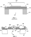
- FIG. 1 depicts a typical conventional art pMUT device 100 formed from multiple thin-film layers deposited onto the substrate 101.
- the device is formed on a substrate 101, e.g., made of silicon but alternative materials such as glass or polymer substrates may be used.
- a bottom layer 102 is formed on a surface of the substrate.
- a bottom electrode layer 104 is sandwiched between the bottom layer 102, and a piezoelectric layer 103.
- a top electrode 106 is formed on the piezoelectric layer 103.
- An opening 107 is formed through the substrate 101 from a backside thereof all the way through to the underside of the bottom layer 102.
- the bottom layer 102 may be made of silicon, silicon dioxide, and/or silicon nitride, among other materials.
- the piezoelectric layer 103 may be composed of various piezoelectric materials including AIN and alloys of AIN such as Sc x Al 1-x N, PZT (lead zirconate titanate) and alloys of PZT such as PLZT and PNZT, ZnO, KNN (K x Na 1-x NbO 3 ) or PMN-PT (lead magnesium niobate - lead titanate).
- Polymer piezoelectric materials such as PVDF may be sometimes be used as piezoelectric layer 103.
- bottom electrode 104 and top electrode 106 Various metals may be used for bottom electrode 104 and top electrode 106 including Al, Au, Pt, Cu, and Mo. Where the bottom layer 102 is made of a sufficiently electrically conductive material, such as doped silicon, the bottom electrode layer 104 may be omitted.
- the membrane's stiffness is determined by both the residual stress (e.g. tension or compression) and the membrane's flexural rigidity.
- the flexural rigidity is determined by parameters that can be tightly controlled during the manufacturing process, namely the membrane geometry (e.g. thickness and diameter) and material properties (e.g. Young's modulus and Poission's ratio).
- aspects of this disclosure include a micromachined ultrasonic transducer (MUT), in particular a piezoelectric micromachined ultrasonic transducer (pMUT) having a variable thickness structure that includes portions of the piezoelectric layer and electrode layer(s).
- MUT micromachined ultrasonic transducer
- pMUT piezoelectric micromachined ultrasonic transducer
- rib-like structures substantially maintain the flexural rigidity of the membrane, but substantially reduce the contribution of the piezo stack's residual stress on the membrane stiffness.
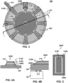
- FIG. 2 and FIGs. 4A-4B are cross-section illustrations of portions of a pMUT device 200 in accordance with aspects of the present disclosure.
- FIG. 3 is a corresponding plan view of the device.
- the device 200 may be formed from multiple thin-film layers deposited onto a substrate 201.
- the substrate 201 may be silicon but alternative materials such as glass or polymer substrates may be used.
- An opening 207 may be formed though the substrate 201.
- a sacrificial layer 202 is formed on a surface of the substrate 201. Sacrificial layer 202 may be made of various materials such as silicon dioxide, and the thickness of this layer is in the range of 0.1 ⁇ m to 4 ⁇ m.
- An elastic layer 204 is formed on the sacrificial layer 202 and over the opening 207 in the substrate 201.
- the elastic layer 204 may be made of silicon, silicon dioxide, and/or silicon nitride, among other materials.
- the elastic layer 204 may be made of polycrystalline silicon (polysilicon).
- the elastic layer 204 may be anchored directly to the substrate 201 at one or more anchors 213 formed through openings in the sacrificial layer ' 202.
- a thickness of the elastic layer 204 may range from, e.g., about 1 ⁇ m to about 20 ⁇ m for transducers with center frequency from 40 kHz to 30 MHz, and more specifically from 1 ⁇ m to 20 ⁇ m for transducers with center frequency from 40 kHz to 1 MHz.
- a small vent opening 205 may be formed through the membrane layer to facilitate equalization of pressure between the two sides of the membrane layer.
- the vent opening 205 is generally relatively small compared to the size of the opening 207.
- the diameter of the opening 205 may be between 2 ⁇ m to 50 ⁇ m. It is generally desirable to locate the vent opening in some place where there is not much stress in the membrane 204, which may not necessarily be true at the center.
- vent openings are described, e.g., in U.S. Patent Application Number 15/141,746 filed April 28, 2016 (published as Patent Application Publication Number 20170021391 ), U.S. Patent Application Number 15/625,421 filed June 16, 2017 (now US 11,005,025 B1 ), and International Patent Application Number PCT/US17/36613 filed June 8, 2017 (published as WO 2017/218299 A1 ).
- An actuating structure layer 206 is formed on a surface of the membrane layer 204.
- the actuating structure layer 206 includes a lower electrode layer 208 sandwiched between the elastic layer 204 and a piezoelectric layer 210, which is sandwiched between the lower electrode layer 208 and an upper electrode layer 212.
- the bottom and top electrode layers may be made of various metals such as Mo, Pt, or Al, and the thickness of these layers may range from 50 nm to 500 nm and more specifically from 100 nm to 300 nm.
- the piezoelectric layer 210 is formed over the bottom electrode 208.
- the bottom electrode layer 208 may also extend beyond the piezoelectric layer 210 and cover portions of the elastic layer 204.
- the piezoelectric layer 210 may be made of various piezoelectric materials including aluminum nitride (AIN) and its alloys such as ScAIN, lead zirconate titanate (PZT) and its alloys such as PLZT and PNZT, zinc oxide (ZnO), K x Na 1-x NbO 3 (KNN) or lead magnesium niobate - lead titanate (PMN-PT).
- AIN aluminum nitride
- PZT lead zirconate titanate
- PNZT zinc oxide
- ZnO zinc oxide
- KNN K x Na 1-x NbO 3
- PMN-PT lead magnesium niobate - lead titanate
- Polymer piezoelectric materials such as PVDF may be used as piezoelectric layer 210 as well.
- the thickness of piezoelectric layer 210 may range from about 250 nm to about 3000 nm, more specifically from about 500 nm to about 1500 nm.
- the combination of the elastic layer 204 and the actuating structure 206 forms a flexing part of the device 200.
- this flexing combination is referred to herein as the membrane.
- the actuating structure layer 206 is patterned to form an actuating structure having a central portion 206C proximate a center of the membrane, rib portions 206R projecting radially and extending to the edge or beyond the edge of the membrane, and open portions 206' that are free of the piezoelectric layer 210 and electrode layers 208, 212.
- Each of the open portions borders the central portion and at least two of the rib portions.
- a ratio of a diameter of central portion 206C to a diameter of the membrane may be between 0.4 and 0.8, e.g., about 0.6.
- the rib portions 206R may include one or more tapered rib portions. By way of example, and not by way of limitation, such tapered rib portions may be wider proximate the edge of the membrane than at the central portion 206C.
- a protective passivation layer 214 may be formed over the actuating structure 206 to encapsulate and protect the lower electrode 208, upper electrode 212, and piezoelectric layer 210 from corrosion e.g. due to humidity. In some embodiments this passivation layer may extend over otherwise exposed portions of the membrane 204 in the open portions 206'. Electrical connections to the electrodes may be made through contacts 216, 218, respectively, formed in openings in the passivation layer 214.
- FIGs. 4A-4B show the cross-sectional structure of one of the rib portions 206R depicted in FIG. 3 .
- the passivation layer 214 is not shown in FIG. 3 .
- a top view of a rib portion 206R is shown in FIG. 4C .
- the membrane's stiffness has two components, the first being the flexural rigidity of the membrane layers (e.g., the elastic layer 204 and the actuating layers 206 ) and the second being the tensile or compressive stress in these layers.
- the presence of the rib portions 206R keeps the flexural rigidity of the membrane comparable to a continuous, unpatterned membrane.
- the absence of the actuating structure 206 (piezoelectric layer 210, top electrode 212 and bottom electrode 208 ) in the open portions of the membrane reduces the contribution of the stress in these layers to the stiffness of the membrane.
- FIG. 3 illustrates and example of a partially fabricated pMUT device 200 showing the patterned lower electrode layer 208 formed on the membrane layer 204.
- This example illustrates the device 200 at an intermediate stage of fabrication after the upper electrode 212 has been formed and patterned on the piezoelectric layer 210, after which the piezoelectric layer 210 has been patterned and finally the exposed bottom electrode layer 208 has been patterned, and the resulting actuating structure 206 has been fully encapsulated by the passivation layer 214.
- the electrode layers 208, 212 and piezoelectric layer 210 may be patterned to define central portions 208C, 212C proximate a center of the membrane, and rib portions 208R, 210R, 212R projecting radially outward from the center portion 208C, 212C and extending to or beyond the anchors 213 that support the membrane edges, e.g., as seen in FIG. 4B .
- At least one rib portion is electrically connected to the center portion and to a contact 215 while the other rib portions may be electrically isolated from the center portion since these rib portions do not contribute the actuation or sensing of vibration in the membrane.
- Lower electrode portions 208C, 208R are denoted by dashed lines in FIG. 3 .
- the membrane 204 is not covered by the electrode layers.
- aspects of the present disclosure are not limited to such implementations and generally encompass implementations in which there are more than three open portions, e.g., four or more, six or more, eight or more.
- the membrane 204 is covered by the passivation layer 214 in the open portions.
- aspects of the present disclosure are not limited to such implementations and include implementations in which there is no passivation layer over the membrane in the open portions.
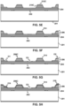
- a pMUT device of the type depicted in FIGs. 2-4C may be fabricated in accordance with aspects of the present disclosure, e.g., as illustrated in FIGs. 5A-5L .
- fabrication may start with a substrate 201 having the sacrificial layer 202 formed thereon.
- the sacrificial layer may be formed by any suitable deposition or growth technique for the relevant material.
- Deposition techniques include physical vapor deposition (PVD) and chemical vapor deposition (CVD). Growth techniques include thermal oxidation (e.g., where the sacrificial layer is an oxide of the substrate material).
- the sacrificial layer 202 may be patterned to define anchor point openings 211, as shown in FIG. 5B . Such patterning may be accomplished with a conventional lithography followed by a suitable etch to form openings through the passivation layer 202 to the surface of the substrate 201.
- the elastic layer 204 may be formed over the sacrificial layer 202, e.g., in a CVD or epitaxial reactor.
- the presence of the anchor point openings 211 facilitates attachment of the membrane layer 204 to the substrate 201 by anchors 213.
- the elastic layer 204 is then polished, e.g. using chemmechanical polishing (CMP), to achieve a low surface roughness in preparation for deposition of the piezoelectric actuation structure.
- CMP chemmechanical polishing
- the lower electrode layer 208 is then formed, e.g., by a metal deposition technique such as PVD.
- a seed layer 208S e.g., of AlN, may be formed on the elastic layer 204 and the metal of the lower electrode layer 208 may be formed on the seed layer.
- the piezoelectric layer 210 is formed on top of the lower electric layer 208 using a deposition technique such as PVD or chemical solution deposition, also known as sol-gel deposition.
- the upper electrode layer 212 is then formed over the piezoelectric layer 210, e.g., by a metal deposition technique such as PVD, and is then patterned to form a central area 212C and rib portions 212R.
- the piezoelectric layer 210 is then patterned as shown in FIG. 5D , e.g., using an etching process that stops on the lower electrode layer 208.
- the lower electrode layer 208 is then patterned as shown in FIG. 5E thereby defining the central portion 208C.
- the passivation layer 214 is deposited, encapsulating the upper electrode layer 212, the piezoelectric layer 210, and the lower electrode layer 208 as shown in FIG. 5E .
- the passivation material 214 may be aluminum nitride (AIN), silicon nitride (Si 3 N 4 ), silicon carbide (SiC) or another dielectric material..
- the passivation layer 214 may be subsequently removed from the open portions of the elastic layer 204 not covered by the upper electrode layer 212, the piezoelectric layer 210, and the lower electrode layer 208. As shown in FIG. 5G , Openings O1, O2 may be formed through the passivation layer 214 to allow for electrical contacts to the upper electrode 212 and lower electrode 208. An additional opening O3 may be formed though the passivation layer to define a vent opening.
- Conductive contacts 216, 218 may be formed to the lower electrode 208 and upper electrode 212, as shown in FIG. 5H .
- the contacts 216, 218 may be made of a corrosion-resistant material such as gold.
- a vent opening 205 may formed through the membrane layer 204 and any overlying layer, such as the piezoelectric layer 210.
- the device may then be finished as shown in FIGs. 5I-5K .
- a vent opening may be formed through the elastic layer 204 to the sacrificial layer 202, as shown in FIG. 5I .
- a protective layer 218, e.g., an oxide may be formed over the front side of the device and the opening 207 may be formed through the substrate, e.g., by etching the substrate from the backside, stopping on the sacrificial layer 202, as shown in FIG. 5J .
- Any suitable isotropic or anisotropic etch process for the substrate material may be used, for example deep reactive ion etching (DRIE) when substrate 201 is composed of silicon.
- DRIE deep reactive ion etching
- the protective layer prevents damage to the structures formed on the membrane during the etch process.
- the sacrificial layer 202 and the protective layer 218 may then be removed, e.g. by etching in hydrofluoric acid (HF) or vapor phase hydrofluoric acid (VHF) as shown in FIG. 5K .
- HF hydrofluoric acid
- VHF vapor phase hydrofluoric acid
- the lower electrode layer 208 may be omitted if the membrane 204 is made of a sufficiently electrically conductive material and the device is intended to operate with the lower electrode grounded to the substrate 201. In such implementations, the membrane itself may act as the lower electrode.
Landscapes
- Engineering & Computer Science (AREA)
- Manufacturing & Machinery (AREA)
- Physics & Mathematics (AREA)
- Acoustics & Sound (AREA)
- Signal Processing (AREA)
- Mechanical Engineering (AREA)
- Transducers For Ultrasonic Waves (AREA)
- Micromachines (AREA)
Claims (14)
- Dispositif transducteur ultrasonore micro-usiné piézoélectrique (200), comprenant:un substrat (201) présentant une cavité ouverte (207);une membrane (204) fixée au substrat de sorte qu'une partie de la membrane recouvre la cavité ouverte, dans lequel la membrane est fixée au substrat au niveau d'une ou de plusieurs parties d'ancrage (213) de la membrane à proximité du périmètre de la cavité ouverte; etune structure d'actionnement (206) sur une surface de la membrane, la structure d'actionnement comportant une couche piézoélectrique (210) prise en sandwich entre la membrane et une couche d'électrode supérieure (212), dans lequel la structure d'actionnement est structurée de sorte que des parties de la structure d'actionnement sont retirées sélectivement de parties de la membrane pour former une partie centrale circulaire (206C) à proximité d'un centre de la cavité ouverte et trois parties de nervure (206R) ou plus se projetant radialement vers l'extérieur à partir de la partie centrale.
- Dispositif selon la revendication 1, dans lequel une ou plusieurs des trois nervures ou plus sont structurées de sorte qu'elles sont mécaniquement couplées à la partie centrale mais électriquement isolées de la partie centrale.
- Dispositif selon la revendication 1, dans lequel la structure d'actionnement est encapsulée par une couche de passivation (214).
- Dispositif selon la revendication 3, dans lequel la couche de passivation est structurée de sorte qu'elle est sensiblement retirée des parties de la membrane non recouvertes par les couches de structure d'actionnement.
- Dispositif selon la revendication 1, dans lequel les trois nervures ou plus comportentquatre parties de nervure ou plus; ousix parties de nervure ou plus; ouhuit parties de nervure ou plus; ouune ou plusieurs parties de nervure effilées; ouune ou plusieurs parties de nervure effilées qui sont plus larges à proximité du périmètre de la membrane qu'au niveau de la partie centrale.
- Dispositif selon la revendication 1, dans lequel la couche de membrane est perforée d'un ou de plusieurs trous qui traversent la structure d'actionnement et la couche de membrane.
- Dispositif selon la revendication 1, dans lequel la structure d'actionnement comporte une couche d'électrode inférieure (208) prise en sandwich entre la couche piézoélectrique et la membrane.
- Dispositif selon la revendication 1, dans lequel le périmètre de la cavité ouverte est de forme circulaire.
- Dispositif selon la revendication 1, dans lequel le périmètre de la cavité ouverte est de forme carrée.
- Dispositif selon la revendication 1, dans lequel une forme de la membrane est une forme polygonale.
- Dispositif selon la revendication 1, comprenant en outre une ouverture (205) formée à travers la partie centrale de la structure d'actionnement et à travers une partie sous-jacente de la membrane jusqu'à la cavité ouverte.
- Dispositif selon la revendication 1, dans lequel un rapport d'un rayon de la partie centrale à un rayon du périmètre est compris entre 0,4 et 0,8.
- Dispositif selon la revendication 1, dans lequel un rapport d'un rayon de la partie centrale à un rayon du périmètre est d'environ 0,6.
- Procédé de fabrication d'un dispositif transducteur ultrasonore micro-usiné piézoélectrique (200), comprenant:la formation d'une membrane (204) fixée à un substrat (201);la formation d'une structure d'actionnement (206) sur une surface de la membrane, la couche de structure d'actionnement comportant une couche piézoélectrique (210) prise en sandwich entre la membrane et une couche d'électrode supérieure (212);la structuration de la structure d'actionnement pour retirer sélectivement des parties de la structure d'actionnement des parties de la membrane pour former une partie centrale circulaire (206C) à proximité d'un centre de la cavité ouverte et trois parties de nervure (206R) ou plus se projetant radialement vers l'extérieur à partir de la partie centrale; etla formation d'une ouverture (207) à travers une partie du substrat sous-jacente à la membrane et à la structure d'actionnement pour définir une cavité ouverte de sorte qu'une ou plusieurs parties d'ancrage (213) de la membrane se trouvent à proximité d'un périmètre de la cavité ouverte.
Applications Claiming Priority (1)
| Application Number | Priority Date | Filing Date | Title |
|---|---|---|---|
| PCT/US2017/062059 WO2019099013A1 (fr) | 2017-11-16 | 2017-11-16 | Transducteur ultrasonore micro-usiné piézoélectrique avec une structure de membrane à motifs |
Publications (3)
| Publication Number | Publication Date |
|---|---|
| EP3676025A1 EP3676025A1 (fr) | 2020-07-08 |
| EP3676025A4 EP3676025A4 (fr) | 2021-04-07 |
| EP3676025B1 true EP3676025B1 (fr) | 2024-08-14 |
Family
ID=66539829
Family Applications (1)
| Application Number | Title | Priority Date | Filing Date |
|---|---|---|---|
| EP17931996.7A Active EP3676025B1 (fr) | 2017-11-16 | 2017-11-16 | Transducteur ultrasonore micro-usiné piézoélectrique avec une structure de membrane à motifs, et une méthode de fabrication |
Country Status (3)
| Country | Link |
|---|---|
| US (2) | US11844282B2 (fr) |
| EP (1) | EP3676025B1 (fr) |
| WO (1) | WO2019099013A1 (fr) |
Families Citing this family (16)
| Publication number | Priority date | Publication date | Assignee | Title |
|---|---|---|---|---|
| EP3233311B1 (fr) * | 2014-12-21 | 2021-12-08 | Chirp Microsystems, Inc. | Transducteurs ultrasoniques micro-usinés piézoélectriques à sensibilité réduite à la contrainte et procédés de fabrication |
| EP3676025B1 (fr) | 2017-11-16 | 2024-08-14 | InvenSense, Inc. | Transducteur ultrasonore micro-usiné piézoélectrique avec une structure de membrane à motifs, et une méthode de fabrication |
| EP3754733A1 (fr) * | 2019-06-19 | 2020-12-23 | Albert-Ludwigs-Universität Freiburg | Actionneur piézoélectrique et dispositif microfluidique |
| IT202000004777A1 (it) | 2020-03-06 | 2021-09-06 | St Microelectronics Srl | Trasduttore ultrasonico microlavorato piezoelettrico |
| US11498097B2 (en) | 2020-05-21 | 2022-11-15 | Vanguard International Semiconductor Corporation | Piezoelectric micromachined ultrasonic transducer and method of fabricating the same |
| CN113896165B (zh) * | 2020-07-06 | 2025-12-16 | 世界先进积体电路股份有限公司 | 压电微机械超声波换能器及其制作方法 |
| TWI747362B (zh) * | 2020-07-06 | 2021-11-21 | 世界先進積體電路股份有限公司 | 壓電微機械超聲波換能器及其製作方法 |
| DE102021213754A1 (de) | 2021-05-28 | 2022-12-15 | Robert Bosch Gesellschaft mit beschränkter Haftung | Verfahren zur Herstellung eines mikro-elektronisch-mechanischen Schwingungssystems und Piezoelektrischer mikrogefertigter Ultraschallwandler |
| CN114543715A (zh) * | 2022-02-18 | 2022-05-27 | 上海声动微科技有限公司 | 超声波传感器以及制作方法 |
| CN115148893B (zh) * | 2022-07-28 | 2025-09-19 | 西安交通大学 | 一种具有弯曲和扭转变形功能的柔性PMUTs及其制备方法 |
| JPWO2024070112A1 (fr) * | 2022-09-30 | 2024-04-04 | ||
| CN118023099A (zh) * | 2022-11-03 | 2024-05-14 | 广州乐仪投资有限公司 | 具有减薄部的pmut结构、其制造方法及包含其的电子设备 |
| SE545977C2 (en) * | 2022-12-22 | 2024-04-02 | Myvox Ab | A Micro-Electromechanical-System based Micro Speaker |
| US12465948B2 (en) * | 2023-02-09 | 2025-11-11 | Stmicroelectronics International N.V. | PMUT array with presence of separate sensing small PZT on membranes edge |
| CN116828367B (zh) * | 2023-06-25 | 2024-08-23 | 联合微电子中心有限责任公司 | 用于声学换能器的电学调控方法和声学换能器及制造方法 |
| WO2025057375A1 (fr) * | 2023-09-14 | 2025-03-20 | 三菱電機株式会社 | Transducteur ultrasonore mems et capteur de distance ultrasonore |
Family Cites Families (21)
| Publication number | Priority date | Publication date | Assignee | Title |
|---|---|---|---|---|
| US2910545A (en) | 1954-08-30 | 1959-10-27 | Gen Electric | Transducer |
| US5828394A (en) | 1995-09-20 | 1998-10-27 | The Board Of Trustees Of The Leland Stanford Junior University | Fluid drop ejector and method |
| US6249075B1 (en) | 1999-11-18 | 2001-06-19 | Lucent Technologies Inc. | Surface micro-machined acoustic transducers |
| JP2006036432A (ja) | 2004-07-26 | 2006-02-09 | Oki Data Corp | 画像形成装置 |
| JP4622574B2 (ja) * | 2005-02-21 | 2011-02-02 | 株式会社デンソー | 超音波素子 |
| JP4844411B2 (ja) | 2006-02-21 | 2011-12-28 | セイコーエプソン株式会社 | 静電型超音波トランスデューサ、静電型超音波トランスデューサの製造方法、超音波スピーカ、音声信号再生方法、超指向性音響システム及び表示装置 |
| JP4946796B2 (ja) | 2007-10-29 | 2012-06-06 | ヤマハ株式会社 | 振動トランスデューサおよび振動トランスデューサの製造方法 |
| EP2669019A1 (fr) | 2009-03-26 | 2013-12-04 | Norwegian University of Science and Technology (NTNU) | Structure d'amortissement acoustique destinée à être utilisée dans un transducteur à ultrasons |
| US7888844B2 (en) | 2009-06-30 | 2011-02-15 | Avago Technologies Wireless Ip (Singapore) Pte. Ltd. | Temperature control of micromachined transducers |
| US9327316B2 (en) | 2009-06-30 | 2016-05-03 | Avago Technologies General Ip (Singapore) Pte. Ltd. | Multi-frequency acoustic array |
| CN103460721B (zh) | 2011-03-31 | 2017-05-24 | 韦斯伯技术公司 | 具有间隙控制几何形状的声换能器以及声换能器制造方法 |
| WO2012145278A2 (fr) * | 2011-04-19 | 2012-10-26 | Eastman Kodak Company | Transducteur composite mems comprenant une membrane souple |
| US9925561B2 (en) | 2013-03-05 | 2018-03-27 | The University Of Manitoba | Capacitive micromachined ultrasonic transducer with multiple deflectable membranes |
| DE102013114826A1 (de) * | 2013-12-23 | 2015-06-25 | USound GmbH | Mikro-elektromechanischer Schallwandler mit schallenergiereflektierender Zwischenschicht |
| EP3110628B1 (fr) | 2014-02-28 | 2019-07-03 | The Regents of the University of California | Diaphragme d'épaisseur variable pour un transducteur ultrasonore micro-usiné piézoélectrique robuste à large bande |
| WO2015171224A1 (fr) * | 2014-05-09 | 2015-11-12 | Chirp Microsystems, Inc. | Transducteur à ultrasons micro-usiné utilisant de multiples matériaux piézoélectriques |
| WO2016054447A1 (fr) * | 2014-10-02 | 2016-04-07 | Chirp Microsystems | Transducteurs ultrasoniques micro-usinés ayant une structure de membrane à fentes |
| EP3233311B1 (fr) * | 2014-12-21 | 2021-12-08 | Chirp Microsystems, Inc. | Transducteurs ultrasoniques micro-usinés piézoélectriques à sensibilité réduite à la contrainte et procédés de fabrication |
| US10618079B2 (en) * | 2016-02-29 | 2020-04-14 | Qualcomm Incorporated | Piezoelectric micromechanical ultrasonic transducers and transducer arrays |
| EP3676025B1 (fr) | 2017-11-16 | 2024-08-14 | InvenSense, Inc. | Transducteur ultrasonore micro-usiné piézoélectrique avec une structure de membrane à motifs, et une méthode de fabrication |
| EP3727708B1 (fr) * | 2017-12-22 | 2024-02-07 | InvenSense, Inc. | Procédé visant à accorder une fréquence de résonance d'un transducteur piézoélectrique micro-usiné |
-
2017
- 2017-11-16 EP EP17931996.7A patent/EP3676025B1/fr active Active
- 2017-11-16 WO PCT/US2017/062059 patent/WO2019099013A1/fr not_active Ceased
-
2020
- 2020-02-26 US US16/802,436 patent/US11844282B2/en active Active
-
2023
- 2023-10-17 US US18/381,104 patent/US12284920B2/en active Active
Also Published As
| Publication number | Publication date |
|---|---|
| US20240049602A1 (en) | 2024-02-08 |
| US11844282B2 (en) | 2023-12-12 |
| EP3676025A4 (fr) | 2021-04-07 |
| WO2019099013A1 (fr) | 2019-05-23 |
| US12284920B2 (en) | 2025-04-22 |
| EP3676025A1 (fr) | 2020-07-08 |
| US20200194658A1 (en) | 2020-06-18 |
Similar Documents
| Publication | Publication Date | Title |
|---|---|---|
| US12284920B2 (en) | Piezoelectric micromachined ultrasonic transducer with a patterned membrane structure | |
| EP3233311B1 (fr) | Transducteurs ultrasoniques micro-usinés piézoélectriques à sensibilité réduite à la contrainte et procédés de fabrication | |
| US11950052B2 (en) | Acoustic transducer with gap-controlling geometry and method of manufacturing an acoustic transducer | |
| EP3201122B1 (fr) | Transducteurs ultrasoniques micro-usinés ayant une structure de membrane à fentes | |
| US10576500B2 (en) | Piezoelectric micro-machined ultrasonic transducer (PMUT) and method for manufacturing the PMUT | |
| KR101562339B1 (ko) | 압전형 마이크로 스피커 및 그 제조 방법 | |
| US7770279B2 (en) | Electrostatic membranes for sensors, ultrasonic transducers incorporating such membranes, and manufacturing methods therefor | |
| EP3472829B1 (fr) | Transducteurs à ultrasons micro-usinés piézoélectriques ayant des caractéristiques de soulagement des contraintes | |
| US8357981B2 (en) | Transducer devices having different frequencies based on layer thicknesses and method of fabricating the same | |
| JP2012529207A (ja) | マイクロメカニカルマイクロフォン構造体を有する素子、および、マイクロメカニカルマイクロフォン構造体を有する素子の製造方法 | |
| JP5961697B2 (ja) | プラグを備える事前圧壊された容量マイクロマシン・トランスデューサセル | |
| CN113301484B (zh) | 一种mems结构及其制造方法 | |
| CN103917304A (zh) | 具有应力层的预塌陷电容式微加工换能器单元 | |
| CN116349249A (zh) | 一种骨传导传声装置 | |
| CN112492472B (zh) | 压电式麦克风及压电式麦克风装置 | |
| US11890643B2 (en) | Piezoelectric micromachined ultrasonic transducer and method of fabricating the same | |
| US11498097B2 (en) | Piezoelectric micromachined ultrasonic transducer and method of fabricating the same | |
| CN115332435B (zh) | 一种含有双极性压电结构的pmut器件及其制备方法 | |
| CN111246356B (zh) | 一种mems结构及其形成方法 | |
| CN113896165B (zh) | 压电微机械超声波换能器及其制作方法 | |
| TW202209718A (zh) | 壓電微機械超聲波換能器及其製作方法 | |
| CN114105082B (zh) | 压电微机械超声波换能器及其制作方法 | |
| TWI747362B (zh) | 壓電微機械超聲波換能器及其製作方法 | |
| CN112838158A (zh) | 压电换能及压电换能器器的制备方法 |
Legal Events
| Date | Code | Title | Description |
|---|---|---|---|
| STAA | Information on the status of an ep patent application or granted ep patent |
Free format text: STATUS: THE INTERNATIONAL PUBLICATION HAS BEEN MADE |
|
| PUAI | Public reference made under article 153(3) epc to a published international application that has entered the european phase |
Free format text: ORIGINAL CODE: 0009012 |
|
| STAA | Information on the status of an ep patent application or granted ep patent |
Free format text: STATUS: REQUEST FOR EXAMINATION WAS MADE |
|
| 17P | Request for examination filed |
Effective date: 20200330 |
|
| AK | Designated contracting states |
Kind code of ref document: A1 Designated state(s): AL AT BE BG CH CY CZ DE DK EE ES FI FR GB GR HR HU IE IS IT LI LT LU LV MC MK MT NL NO PL PT RO RS SE SI SK SM TR |
|
| AX | Request for extension of the european patent |
Extension state: BA ME |
|
| DAV | Request for validation of the european patent (deleted) | ||
| DAX | Request for extension of the european patent (deleted) | ||
| A4 | Supplementary search report drawn up and despatched |
Effective date: 20210309 |
|
| RIC1 | Information provided on ipc code assigned before grant |
Ipc: B06B 1/06 20060101AFI20210302BHEP Ipc: H01L 41/083 20060101ALI20210302BHEP Ipc: H01L 41/09 20060101ALI20210302BHEP Ipc: H01L 41/08 20060101ALI20210302BHEP |
|
| RAP1 | Party data changed (applicant data changed or rights of an application transferred) |
Owner name: INVENSENSE, INC. |
|
| REG | Reference to a national code |
Ref country code: DE Ref legal event code: R079 Ipc: H10N0030500000 Ref country code: DE Ref legal event code: R079 Ref document number: 602017084172 Country of ref document: DE Free format text: PREVIOUS MAIN CLASS: B06B0001060000 Ipc: H10N0030500000 |
|
| RIC1 | Information provided on ipc code assigned before grant |
Ipc: B06B 1/06 20060101ALI20231129BHEP Ipc: H10N 30/00 20230101ALI20231129BHEP Ipc: H10N 30/50 20230101AFI20231129BHEP |
|
| REG | Reference to a national code |
Ref country code: DE Ref legal event code: R079 Free format text: PREVIOUS MAIN CLASS: H10N0030500000 Ipc: H10N0030010000 Ref country code: DE Ref legal event code: R079 Ref document number: 602017084172 Country of ref document: DE Free format text: PREVIOUS MAIN CLASS: H10N0030500000 Ipc: H10N0030010000 |
|
| RIC1 | Information provided on ipc code assigned before grant |
Ipc: B06B 1/06 20060101ALI20240119BHEP Ipc: H10N 30/30 20230101ALI20240119BHEP Ipc: H10N 30/01 20230101AFI20240119BHEP |
|
| GRAP | Despatch of communication of intention to grant a patent |
Free format text: ORIGINAL CODE: EPIDOSNIGR1 |
|
| STAA | Information on the status of an ep patent application or granted ep patent |
Free format text: STATUS: GRANT OF PATENT IS INTENDED |
|
| RIC1 | Information provided on ipc code assigned before grant |
Ipc: B06B 1/06 20060101ALI20240219BHEP Ipc: H10N 30/20 20230101ALI20240219BHEP Ipc: H10N 30/01 20230101AFI20240219BHEP |
|
| INTG | Intention to grant announced |
Effective date: 20240306 |
|
| GRAS | Grant fee paid |
Free format text: ORIGINAL CODE: EPIDOSNIGR3 |
|
| GRAA | (expected) grant |
Free format text: ORIGINAL CODE: 0009210 |
|
| STAA | Information on the status of an ep patent application or granted ep patent |
Free format text: STATUS: THE PATENT HAS BEEN GRANTED |
|
| P01 | Opt-out of the competence of the unified patent court (upc) registered |
Free format text: CASE NUMBER: APP_33979/2024 Effective date: 20240606 |
|
| AK | Designated contracting states |
Kind code of ref document: B1 Designated state(s): AL AT BE BG CH CY CZ DE DK EE ES FI FR GB GR HR HU IE IS IT LI LT LU LV MC MK MT NL NO PL PT RO RS SE SI SK SM TR |
|
| REG | Reference to a national code |
Ref country code: GB Ref legal event code: FG4D |
|
| REG | Reference to a national code |
Ref country code: CH Ref legal event code: EP |
|
| REG | Reference to a national code |
Ref country code: DE Ref legal event code: R096 Ref document number: 602017084172 Country of ref document: DE |
|
| REG | Reference to a national code |
Ref country code: IE Ref legal event code: FG4D |
|
| REG | Reference to a national code |
Ref country code: LT Ref legal event code: MG9D |
|
| REG | Reference to a national code |
Ref country code: NL Ref legal event code: MP Effective date: 20240814 |
|
| PG25 | Lapsed in a contracting state [announced via postgrant information from national office to epo] |
Ref country code: NO Free format text: LAPSE BECAUSE OF FAILURE TO SUBMIT A TRANSLATION OF THE DESCRIPTION OR TO PAY THE FEE WITHIN THE PRESCRIBED TIME-LIMIT Effective date: 20241114 |
|
| REG | Reference to a national code |
Ref country code: AT Ref legal event code: MK05 Ref document number: 1714507 Country of ref document: AT Kind code of ref document: T Effective date: 20240814 |
|
| PG25 | Lapsed in a contracting state [announced via postgrant information from national office to epo] |
Ref country code: NL Free format text: LAPSE BECAUSE OF FAILURE TO SUBMIT A TRANSLATION OF THE DESCRIPTION OR TO PAY THE FEE WITHIN THE PRESCRIBED TIME-LIMIT Effective date: 20240814 Ref country code: FI Free format text: LAPSE BECAUSE OF FAILURE TO SUBMIT A TRANSLATION OF THE DESCRIPTION OR TO PAY THE FEE WITHIN THE PRESCRIBED TIME-LIMIT Effective date: 20240814 Ref country code: PL Free format text: LAPSE BECAUSE OF FAILURE TO SUBMIT A TRANSLATION OF THE DESCRIPTION OR TO PAY THE FEE WITHIN THE PRESCRIBED TIME-LIMIT Effective date: 20240814 Ref country code: GR Free format text: LAPSE BECAUSE OF FAILURE TO SUBMIT A TRANSLATION OF THE DESCRIPTION OR TO PAY THE FEE WITHIN THE PRESCRIBED TIME-LIMIT Effective date: 20241115 Ref country code: PT Free format text: LAPSE BECAUSE OF FAILURE TO SUBMIT A TRANSLATION OF THE DESCRIPTION OR TO PAY THE FEE WITHIN THE PRESCRIBED TIME-LIMIT Effective date: 20241216 |
|
| PG25 | Lapsed in a contracting state [announced via postgrant information from national office to epo] |
Ref country code: BG Free format text: LAPSE BECAUSE OF FAILURE TO SUBMIT A TRANSLATION OF THE DESCRIPTION OR TO PAY THE FEE WITHIN THE PRESCRIBED TIME-LIMIT Effective date: 20240814 |
|
| PG25 | Lapsed in a contracting state [announced via postgrant information from national office to epo] |
Ref country code: LV Free format text: LAPSE BECAUSE OF FAILURE TO SUBMIT A TRANSLATION OF THE DESCRIPTION OR TO PAY THE FEE WITHIN THE PRESCRIBED TIME-LIMIT Effective date: 20240814 |
|
| PG25 | Lapsed in a contracting state [announced via postgrant information from national office to epo] |
Ref country code: AT Free format text: LAPSE BECAUSE OF FAILURE TO SUBMIT A TRANSLATION OF THE DESCRIPTION OR TO PAY THE FEE WITHIN THE PRESCRIBED TIME-LIMIT Effective date: 20240814 Ref country code: IS Free format text: LAPSE BECAUSE OF FAILURE TO SUBMIT A TRANSLATION OF THE DESCRIPTION OR TO PAY THE FEE WITHIN THE PRESCRIBED TIME-LIMIT Effective date: 20241214 |
|
| PG25 | Lapsed in a contracting state [announced via postgrant information from national office to epo] |
Ref country code: HR Free format text: LAPSE BECAUSE OF FAILURE TO SUBMIT A TRANSLATION OF THE DESCRIPTION OR TO PAY THE FEE WITHIN THE PRESCRIBED TIME-LIMIT Effective date: 20240814 |
|
| PG25 | Lapsed in a contracting state [announced via postgrant information from national office to epo] |
Ref country code: RS Free format text: LAPSE BECAUSE OF FAILURE TO SUBMIT A TRANSLATION OF THE DESCRIPTION OR TO PAY THE FEE WITHIN THE PRESCRIBED TIME-LIMIT Effective date: 20241114 Ref country code: ES Free format text: LAPSE BECAUSE OF FAILURE TO SUBMIT A TRANSLATION OF THE DESCRIPTION OR TO PAY THE FEE WITHIN THE PRESCRIBED TIME-LIMIT Effective date: 20240814 |
|
| PG25 | Lapsed in a contracting state [announced via postgrant information from national office to epo] |
Ref country code: RS Free format text: LAPSE BECAUSE OF FAILURE TO SUBMIT A TRANSLATION OF THE DESCRIPTION OR TO PAY THE FEE WITHIN THE PRESCRIBED TIME-LIMIT Effective date: 20241114 Ref country code: PT Free format text: LAPSE BECAUSE OF FAILURE TO SUBMIT A TRANSLATION OF THE DESCRIPTION OR TO PAY THE FEE WITHIN THE PRESCRIBED TIME-LIMIT Effective date: 20241216 Ref country code: PL Free format text: LAPSE BECAUSE OF FAILURE TO SUBMIT A TRANSLATION OF THE DESCRIPTION OR TO PAY THE FEE WITHIN THE PRESCRIBED TIME-LIMIT Effective date: 20240814 Ref country code: NO Free format text: LAPSE BECAUSE OF FAILURE TO SUBMIT A TRANSLATION OF THE DESCRIPTION OR TO PAY THE FEE WITHIN THE PRESCRIBED TIME-LIMIT Effective date: 20241114 Ref country code: NL Free format text: LAPSE BECAUSE OF FAILURE TO SUBMIT A TRANSLATION OF THE DESCRIPTION OR TO PAY THE FEE WITHIN THE PRESCRIBED TIME-LIMIT Effective date: 20240814 Ref country code: LV Free format text: LAPSE BECAUSE OF FAILURE TO SUBMIT A TRANSLATION OF THE DESCRIPTION OR TO PAY THE FEE WITHIN THE PRESCRIBED TIME-LIMIT Effective date: 20240814 Ref country code: IS Free format text: LAPSE BECAUSE OF FAILURE TO SUBMIT A TRANSLATION OF THE DESCRIPTION OR TO PAY THE FEE WITHIN THE PRESCRIBED TIME-LIMIT Effective date: 20241214 Ref country code: HR Free format text: LAPSE BECAUSE OF FAILURE TO SUBMIT A TRANSLATION OF THE DESCRIPTION OR TO PAY THE FEE WITHIN THE PRESCRIBED TIME-LIMIT Effective date: 20240814 Ref country code: GR Free format text: LAPSE BECAUSE OF FAILURE TO SUBMIT A TRANSLATION OF THE DESCRIPTION OR TO PAY THE FEE WITHIN THE PRESCRIBED TIME-LIMIT Effective date: 20241115 Ref country code: FI Free format text: LAPSE BECAUSE OF FAILURE TO SUBMIT A TRANSLATION OF THE DESCRIPTION OR TO PAY THE FEE WITHIN THE PRESCRIBED TIME-LIMIT Effective date: 20240814 Ref country code: ES Free format text: LAPSE BECAUSE OF FAILURE TO SUBMIT A TRANSLATION OF THE DESCRIPTION OR TO PAY THE FEE WITHIN THE PRESCRIBED TIME-LIMIT Effective date: 20240814 Ref country code: BG Free format text: LAPSE BECAUSE OF FAILURE TO SUBMIT A TRANSLATION OF THE DESCRIPTION OR TO PAY THE FEE WITHIN THE PRESCRIBED TIME-LIMIT Effective date: 20240814 Ref country code: AT Free format text: LAPSE BECAUSE OF FAILURE TO SUBMIT A TRANSLATION OF THE DESCRIPTION OR TO PAY THE FEE WITHIN THE PRESCRIBED TIME-LIMIT Effective date: 20240814 |
|
| PG25 | Lapsed in a contracting state [announced via postgrant information from national office to epo] |
Ref country code: RO Free format text: LAPSE BECAUSE OF FAILURE TO SUBMIT A TRANSLATION OF THE DESCRIPTION OR TO PAY THE FEE WITHIN THE PRESCRIBED TIME-LIMIT Effective date: 20240814 Ref country code: SM Free format text: LAPSE BECAUSE OF FAILURE TO SUBMIT A TRANSLATION OF THE DESCRIPTION OR TO PAY THE FEE WITHIN THE PRESCRIBED TIME-LIMIT Effective date: 20240814 Ref country code: DK Free format text: LAPSE BECAUSE OF FAILURE TO SUBMIT A TRANSLATION OF THE DESCRIPTION OR TO PAY THE FEE WITHIN THE PRESCRIBED TIME-LIMIT Effective date: 20240814 |
|
| PG25 | Lapsed in a contracting state [announced via postgrant information from national office to epo] |
Ref country code: EE Free format text: LAPSE BECAUSE OF FAILURE TO SUBMIT A TRANSLATION OF THE DESCRIPTION OR TO PAY THE FEE WITHIN THE PRESCRIBED TIME-LIMIT Effective date: 20240814 |
|
| PG25 | Lapsed in a contracting state [announced via postgrant information from national office to epo] |
Ref country code: CZ Free format text: LAPSE BECAUSE OF FAILURE TO SUBMIT A TRANSLATION OF THE DESCRIPTION OR TO PAY THE FEE WITHIN THE PRESCRIBED TIME-LIMIT Effective date: 20240814 |
|
| PG25 | Lapsed in a contracting state [announced via postgrant information from national office to epo] |
Ref country code: SK Free format text: LAPSE BECAUSE OF FAILURE TO SUBMIT A TRANSLATION OF THE DESCRIPTION OR TO PAY THE FEE WITHIN THE PRESCRIBED TIME-LIMIT Effective date: 20240814 Ref country code: IT Free format text: LAPSE BECAUSE OF FAILURE TO SUBMIT A TRANSLATION OF THE DESCRIPTION OR TO PAY THE FEE WITHIN THE PRESCRIBED TIME-LIMIT Effective date: 20240814 |
|
| REG | Reference to a national code |
Ref country code: DE Ref legal event code: R097 Ref document number: 602017084172 Country of ref document: DE |
|
| PLBE | No opposition filed within time limit |
Free format text: ORIGINAL CODE: 0009261 |
|
| STAA | Information on the status of an ep patent application or granted ep patent |
Free format text: STATUS: NO OPPOSITION FILED WITHIN TIME LIMIT |
|
| REG | Reference to a national code |
Ref country code: CH Ref legal event code: PL |
|
| PG25 | Lapsed in a contracting state [announced via postgrant information from national office to epo] |
Ref country code: MC Free format text: LAPSE BECAUSE OF FAILURE TO SUBMIT A TRANSLATION OF THE DESCRIPTION OR TO PAY THE FEE WITHIN THE PRESCRIBED TIME-LIMIT Effective date: 20240814 |
|
| PG25 | Lapsed in a contracting state [announced via postgrant information from national office to epo] |
Ref country code: LU Free format text: LAPSE BECAUSE OF NON-PAYMENT OF DUE FEES Effective date: 20241116 |
|
| REG | Reference to a national code |
Ref country code: CH Ref legal event code: PL |
|
| 26N | No opposition filed |
Effective date: 20250515 |
|
| GBPC | Gb: european patent ceased through non-payment of renewal fee |
Effective date: 20241116 |
|
| PG25 | Lapsed in a contracting state [announced via postgrant information from national office to epo] |
Ref country code: CH Free format text: LAPSE BECAUSE OF NON-PAYMENT OF DUE FEES Effective date: 20241130 |
|
| REG | Reference to a national code |
Ref country code: BE Ref legal event code: MM Effective date: 20241130 |
|
| PG25 | Lapsed in a contracting state [announced via postgrant information from national office to epo] |
Ref country code: SE Free format text: LAPSE BECAUSE OF FAILURE TO SUBMIT A TRANSLATION OF THE DESCRIPTION OR TO PAY THE FEE WITHIN THE PRESCRIBED TIME-LIMIT Effective date: 20240814 |
|
| PG25 | Lapsed in a contracting state [announced via postgrant information from national office to epo] |
Ref country code: GB Free format text: LAPSE BECAUSE OF NON-PAYMENT OF DUE FEES Effective date: 20241116 Ref country code: BE Free format text: LAPSE BECAUSE OF NON-PAYMENT OF DUE FEES Effective date: 20241130 |
|
| PG25 | Lapsed in a contracting state [announced via postgrant information from national office to epo] |
Ref country code: FR Free format text: LAPSE BECAUSE OF NON-PAYMENT OF DUE FEES Effective date: 20241130 |
|
| PG25 | Lapsed in a contracting state [announced via postgrant information from national office to epo] |
Ref country code: IE Free format text: LAPSE BECAUSE OF NON-PAYMENT OF DUE FEES Effective date: 20241116 |
|
| PGFP | Annual fee paid to national office [announced via postgrant information from national office to epo] |
Ref country code: DE Payment date: 20250923 Year of fee payment: 9 |
|
| PG25 | Lapsed in a contracting state [announced via postgrant information from national office to epo] |
Ref country code: HU Free format text: LAPSE BECAUSE OF FAILURE TO SUBMIT A TRANSLATION OF THE DESCRIPTION OR TO PAY THE FEE WITHIN THE PRESCRIBED TIME-LIMIT; INVALID AB INITIO Effective date: 20171116 |
|
| PG25 | Lapsed in a contracting state [announced via postgrant information from national office to epo] |
Ref country code: CY Free format text: LAPSE BECAUSE OF FAILURE TO SUBMIT A TRANSLATION OF THE DESCRIPTION OR TO PAY THE FEE WITHIN THE PRESCRIBED TIME-LIMIT; INVALID AB INITIO Effective date: 20171116 |