EP3676598B1 - Lasers à haute puissance pour transfert western - Google Patents
Lasers à haute puissance pour transfert western Download PDFInfo
- Publication number
- EP3676598B1 EP3676598B1 EP18850493.0A EP18850493A EP3676598B1 EP 3676598 B1 EP3676598 B1 EP 3676598B1 EP 18850493 A EP18850493 A EP 18850493A EP 3676598 B1 EP3676598 B1 EP 3676598B1
- Authority
- EP
- European Patent Office
- Prior art keywords
- sample
- epi
- laser
- illuminator
- lasers
- Prior art date
- Legal status (The legal status is an assumption and is not a legal conclusion. Google has not performed a legal analysis and makes no representation as to the accuracy of the status listed.)
- Active
Links
Images




Classifications
-
- G—PHYSICS
- G01—MEASURING; TESTING
- G01N—INVESTIGATING OR ANALYSING MATERIALS BY DETERMINING THEIR CHEMICAL OR PHYSICAL PROPERTIES
- G01N21/00—Investigating or analysing materials by the use of optical means, i.e. using sub-millimetre waves, infrared, visible or ultraviolet light
- G01N21/62—Systems in which the material investigated is excited whereby it emits light or causes a change in wavelength of the incident light
- G01N21/63—Systems in which the material investigated is excited whereby it emits light or causes a change in wavelength of the incident light optically excited
- G01N21/64—Fluorescence; Phosphorescence
- G01N21/6428—Measuring fluorescence of fluorescent products of reactions or of fluorochrome labelled reactive substances, e.g. measuring quenching effects, using measuring "optrodes"
-
- G—PHYSICS
- G01—MEASURING; TESTING
- G01N—INVESTIGATING OR ANALYSING MATERIALS BY DETERMINING THEIR CHEMICAL OR PHYSICAL PROPERTIES
- G01N21/00—Investigating or analysing materials by the use of optical means, i.e. using sub-millimetre waves, infrared, visible or ultraviolet light
- G01N21/62—Systems in which the material investigated is excited whereby it emits light or causes a change in wavelength of the incident light
- G01N21/63—Systems in which the material investigated is excited whereby it emits light or causes a change in wavelength of the incident light optically excited
- G01N21/64—Fluorescence; Phosphorescence
- G01N21/645—Specially adapted constructive features of fluorimeters
- G01N21/6456—Spatial resolved fluorescence measurements; Imaging
-
- G—PHYSICS
- G02—OPTICS
- G02B—OPTICAL ELEMENTS, SYSTEMS OR APPARATUS
- G02B5/00—Optical elements other than lenses
- G02B5/02—Diffusing elements; Afocal elements
- G02B5/0205—Diffusing elements; Afocal elements characterised by the diffusing properties
- G02B5/021—Diffusing elements; Afocal elements characterised by the diffusing properties the diffusion taking place at the element's surface, e.g. by means of surface roughening or microprismatic structures
- G02B5/0215—Diffusing elements; Afocal elements characterised by the diffusing properties the diffusion taking place at the element's surface, e.g. by means of surface roughening or microprismatic structures the surface having a regular structure
-
- G—PHYSICS
- G02—OPTICS
- G02B—OPTICAL ELEMENTS, SYSTEMS OR APPARATUS
- G02B5/00—Optical elements other than lenses
- G02B5/02—Diffusing elements; Afocal elements
- G02B5/0205—Diffusing elements; Afocal elements characterised by the diffusing properties
- G02B5/021—Diffusing elements; Afocal elements characterised by the diffusing properties the diffusion taking place at the element's surface, e.g. by means of surface roughening or microprismatic structures
- G02B5/0221—Diffusing elements; Afocal elements characterised by the diffusing properties the diffusion taking place at the element's surface, e.g. by means of surface roughening or microprismatic structures the surface having an irregular structure
-
- G—PHYSICS
- G02—OPTICS
- G02B—OPTICAL ELEMENTS, SYSTEMS OR APPARATUS
- G02B5/00—Optical elements other than lenses
- G02B5/02—Diffusing elements; Afocal elements
- G02B5/0205—Diffusing elements; Afocal elements characterised by the diffusing properties
- G02B5/0252—Diffusing elements; Afocal elements characterised by the diffusing properties using holographic or diffractive means
-
- G—PHYSICS
- G01—MEASURING; TESTING
- G01N—INVESTIGATING OR ANALYSING MATERIALS BY DETERMINING THEIR CHEMICAL OR PHYSICAL PROPERTIES
- G01N21/00—Investigating or analysing materials by the use of optical means, i.e. using sub-millimetre waves, infrared, visible or ultraviolet light
- G01N21/62—Systems in which the material investigated is excited whereby it emits light or causes a change in wavelength of the incident light
- G01N21/63—Systems in which the material investigated is excited whereby it emits light or causes a change in wavelength of the incident light optically excited
- G01N21/64—Fluorescence; Phosphorescence
- G01N21/6428—Measuring fluorescence of fluorescent products of reactions or of fluorochrome labelled reactive substances, e.g. measuring quenching effects, using measuring "optrodes"
- G01N2021/6439—Measuring fluorescence of fluorescent products of reactions or of fluorochrome labelled reactive substances, e.g. measuring quenching effects, using measuring "optrodes" with indicators, stains, dyes, tags, labels, marks
-
- G—PHYSICS
- G01—MEASURING; TESTING
- G01N—INVESTIGATING OR ANALYSING MATERIALS BY DETERMINING THEIR CHEMICAL OR PHYSICAL PROPERTIES
- G01N21/00—Investigating or analysing materials by the use of optical means, i.e. using sub-millimetre waves, infrared, visible or ultraviolet light
- G01N21/62—Systems in which the material investigated is excited whereby it emits light or causes a change in wavelength of the incident light
- G01N21/63—Systems in which the material investigated is excited whereby it emits light or causes a change in wavelength of the incident light optically excited
- G01N21/64—Fluorescence; Phosphorescence
- G01N21/645—Specially adapted constructive features of fluorimeters
- G01N2021/6463—Optics
-
- G—PHYSICS
- G01—MEASURING; TESTING
- G01N—INVESTIGATING OR ANALYSING MATERIALS BY DETERMINING THEIR CHEMICAL OR PHYSICAL PROPERTIES
- G01N2201/00—Features of devices classified in G01N21/00
- G01N2201/06—Illumination; Optics
- G01N2201/061—Sources
- G01N2201/06113—Coherent sources; lasers
- G01N2201/0612—Laser diodes
-
- G—PHYSICS
- G01—MEASURING; TESTING
- G01N—INVESTIGATING OR ANALYSING MATERIALS BY DETERMINING THEIR CHEMICAL OR PHYSICAL PROPERTIES
- G01N2201/00—Features of devices classified in G01N21/00
- G01N2201/06—Illumination; Optics
- G01N2201/063—Illuminating optical parts
- G01N2201/0634—Diffuse illumination
-
- G—PHYSICS
- G02—OPTICS
- G02B—OPTICAL ELEMENTS, SYSTEMS OR APPARATUS
- G02B21/00—Microscopes
- G02B21/16—Microscopes adapted for ultraviolet illumination ; Fluorescence microscopes
-
- G—PHYSICS
- G02—OPTICS
- G02B—OPTICAL ELEMENTS, SYSTEMS OR APPARATUS
- G02B5/00—Optical elements other than lenses
- G02B5/02—Diffusing elements; Afocal elements
- G02B5/0205—Diffusing elements; Afocal elements characterised by the diffusing properties
- G02B5/021—Diffusing elements; Afocal elements characterised by the diffusing properties the diffusion taking place at the element's surface, e.g. by means of surface roughening or microprismatic structures
Definitions
- Electroblotting is a widely used biotechnology technique that involves applying a potential difference across a matrix in which charged analytes, such as DNA, RNA, or protein, are distributed.
- the potential difference causes the analytes to migrate out of the matrix and become deposited on a surface, or "blot", next to the matrix, where they are immobilized.
- the analytes can then be detected using fluorescence, chemiluminescence, radioactivity, or other phenomena, by probing the analytes with one or more detectable binding partners.
- Fluorescence detection is a useful method for western blotting and other electroblotting applications. Proteins immobilized on a surface of a western blotting membrane are commonly labeled with fluorescent markers for specific antibody detection.
- the fluorescent markers can be excited from above by an excitation source, with the fluorescent markers emitting light at a slightly longer wavelength, which is detected by an imaging system.
- Suitable imaging systems, so-called illuminator devices for detection of the light emitted by the fluorescent markers are known from US Patent 6,672,739 , US 2013/0201577 A1 and US 2013/0194787 A1 .
- HDR high dynamic range
- One technique for reducing required imaging times is to increase the intensity of excitation via illumination with an excitation light source.
- the use of an excitation source that can deliver 10-fold greater light intensity to fluorescent markers can be expected to reduce by 10-fold the exposure time required to achieve a particular emission response.
- increases in illumination intensities and powers can be accompanied by technical problems and challenges.
- the use of a high power laser in imaging protocols can introduce significant illumination non-uniformities related to coherence and interference properties of laser light in general, and high power laser beams in particular.
- devices and methods that are characterized by the use of high power lasers for the excitation of samples such as western blots.
- the inventors have discovered that through the use of particular optical diffusers, configurations of multiple lasers, or multiple spatial or temporal laser modalities, epi-illumination of samples with substantially uniform illumination from high power lasers can be achieved.
- the first aspect of the invention provides an epi-illuminator for a sample as defined in independent claim 1, which includes
- the optical diffuser is a holographic diffuser having a diffusing half angle within the range from 3° (degrees) to 70°. In some embodiments, the optical diffuser is a holographic diffuser having a diffusing half angle within the range from 5° to 30°. In some embodiments, the laser has a power within the range from 10 W to 80 W. In some embodiments, the optical diffuser is a ground glass diffuser. In some embodiments, the optical diffuser is an engineered microlens array.
- the laser is a semiconductor vertical-cavity surface-emitting laser (VCSEL) array. In some embodiments, the laser is an edge emitting semiconductor laser or laser array. In some embodiments, the excitation light has a wavelength within the range from 640 nm to 850 nm. In some embodiments the excitation light source includes two or more lasers or laser arrays, wherein each of the two or more lasers or laser arrays has a power within the range from 5 W to 500 W
- the sample side of the planar platform has an area within the range from 10 cm 2 to 500 cm 2 . In some embodiments, the sample side of the planar platform has an area within the range from 50 cm 2 to 200 cm 2 . In some embodiments, the sample is a biological sample. In some embodiments, the sample is a membrane or gel. In some embodiments, the sample is a western blot.
- the second aspect of the invention provides an epi-illuminator as defined in independent claim 8 that includes
- the excitation light source comprises ten or more lasers. In some embodiments, each of the lasers has a power within the range from 5 W to 50 W. In some embodiments, each of the lasers has a power within the range from 10 W to 20 W. In some embodiments, the excitation light source includes 100 or more lasers, wherein each of the 100 or more lasers has a power of less than 100 mW. In some embodiments, the excitation light source is a semiconductor vertical-cavity surface-emitting laser (VCSEL) array. In some embodiments, each of the lasers is an edge emitting semiconductor laser. In some embodiments, the excitation light has a wavelength within the range from 640 nm to 850 nm.
- VCSEL semiconductor vertical-cavity surface-emitting laser
- the sample side of the planar platform has an area within the range from 10 cm 2 to 500 cm 2 . In some embodiments, the sample side of the planar platform has an area within the range from 50 cm 2 to 200 cm 2 . In some embodiments, the sample is a biological sample. In some embodiments, the sample is a membrane or gel. In some embodiments, the sample is a western blot.
- the third aspect of the invention provides a method for imaging a sample, which includes
- the invention described herein generally relates to the use of high power lasers in various configurations for uniformly illuminating samples such as western blots.
- the terms "high power laser” are used to refer to lasers having output powers of greater than 5 W.
- High intensity light such as that produced by high power lasers can be used to produce excitation light capable of generating strong fluorescence emissions from fluorescent markers.
- detected signal intensities from fluorescent markers can be lower, and required exposure times to detect these markers can be longer. See for example FIG. 1 , which shows an image of a dot blot that has been illuminated by LED lights, and FIG. 2 , which shows an example of a dot blot that has been illuminated by high power lasers.
- the high power laser illumination provides high signal intensities of the dot blot spots relative to the background.
- Existing high power laser configurations can fail to address interference and coherence issues with laser light that can cause significant non-uniformities in sample illumination.
- fluorescent samples illuminated by high power lasers can exhibit visible stripe patterns unrelated to the actual sample itself. These patterns are instead caused by interference or coherence of the lasers and their related multi-modalities as described in further detail below.
- FIGS. 2 and 3 present images captured with a provided high power laser configuration in accordance with an embodiment, and an alternate comparative configuration, respectively. It can be seen from FIGS. 2 and 3 that the epi-illuminator of FIG. 2 in accordance with an embodiment produces a more uniform illumination than the comparative epi-illuminator of FIG. 3 which produces an illumination characterized by horizontal banding. Beneficially, the high power laser epi-illuminators produce high emission signal intensities while reducing required imaging exposure times. In particular, the high power lasers do not negatively affect the signal to background ratios of the acquired images, and allow for the detection of fainter fluorescent features than could otherwise be accomplished.
- epi-illuminator refers to a device or system used to illuminate a sample from above or the side, for example on the same side of the sample as a sensor, such that reflected light or fluorescence emission can be detected using the sensor. This is in contrast to illumination from below the sample, or on the opposite side of the sample as the sensor, in which light passing through the sample can be detected using the sensor.
- the illuminating light of the epi-illuminator can be referred to as epi-illumination or episcopic illumination, and the use of fluorescence light in an epi-illuminator can be referred to as epifluorescence.
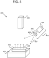
- FIG. 4 illustrates an epi-illuminator in accordance with an embodiment.
- the epi-illuminator 400 includes a planar platform 401 having a sample side that is configured to support a sample 402.
- the epi-illuminator also includes an excitation light source 403 that itself includes a laser 404 and an optical diffuser 405.
- both the laser and optical diffuser are mounted above the planar platform.
- at least the optical diffuser is mounted above the planar platform.
- the optical diffuser is positioned between the laser and the planar platform along the optical path 406 of the laser, such that laser light projected by the laser passes through the optical diffuser and illuminates the sample.
- the epi-illuminator also includes a sensor 408 that is configured to detect fluorescence emission light 409 emitted from the sample.
- the optical diffuser can be, for example and without limitation, a ground glass diffuser, a TEFLON TM diffuser, a holographic diffuser, an opal glass diffuser, a greyed glass diffuser, or a fiber optic diffuser.
- the optical diffuser is a multi-mode optical fiber.
- the optical diffuser is a ground glass diffuser.
- a ground glass diffuser is a diffuser comprising high tolerance and high quality glass that has been ground using one or more polishing blends of various grit sizes. Ground glass diffusers are particularly well suited for applications benefitting from high light transmission, and uniform diffusion across a wide range of directions.
- the optical diffuser is a holographic diffuser.
- a holographic diffuser is diffuser having engineered holographic patterns embedded on its surface material, which can be, for example, polycarbonate, polyester, or other optical polymer.
- the engineered surface of a holographic diffuser is in contrast to the random surface of a ground glass diffuser.
- Holographic diffusers can be characterized by their diffusing half angle, defined as the angle of observation at which a luminance has half the value of the luminance of diffused light at the angle of 0° (degrees), with perpendicular incidence of light.
- the holographic diffuser of the epi-illuminator can have a diffusing half angle within the range from 3° to 70°, e.g., from 3° to 43°, from 10° to 50°, from 16° to 56°, from 23° to 63°, or from 30° to 70°.
- the holographic diffuser can have a diffusing half angle within the range between 5° and 30°, e.g., from 5° to 20°, from 7.5° to 22.5°, from 10° to 25°, from 12.5° to 27.5°, or from 15° to 30°.
- the optical diffuser is an engineered microlens array.
- Such arrays include a plurality of individual microlens units, each of which is configured to have, for example, a preselected sag profile and/or location within the array.
- the distribution of individual microlens units within the array is randomized to minimize diffraction artifacts.
- the engineered microlens array can comprise materials including, for example, silicon, silicon dioxide, germanium, or combinations thereof.
- the engineered microlens array is configured such that excitation light from a side-mounted location is flattened, thereby illuminating the sample side of an epi-illuminator planar platform with substantially uniform light intensity.
- Each of the spatial modes can have a particular beam pattern that can include any number or horizontal, vertical, or curved lines; or geometric shapes such as circles, squares, rectangles, or triangles. It is noted that in some cases, and as is shown in FIG. 3 , the multiple spatial modes can interfere with one another and give rise to non-uniform illumination. However, in the claimed invention, the different spatial modes are specifically chosen and configured to produce a combined illumination that is spatially incoherent, thus providing substantially uniform light intensity across the illuminated surface or object.
- the term "substantially uniform light intensity" can refer to an illumination of an area wherein the illumination intensity at any point within the area differs by less than 20% from the average illumination intensity at all points of the area.
- the illumination intensity at any point can be, for example, 20% less than, 18% less than, 16% less than, 14% less than, 12% less than, 10% less than. 8% less than, 6% less than, 4% less than, 2% less than, identical to, 2% greater than, 4% greater than, 6% greater than, 8% greater than, 10% greater than, 12% greater than, 14% greater than, 16% greater than, 18% greater than, or 20% greater than the average illumination intensity.
- substantially uniform light intensity can refer to an illumination of an area wherein the illumination intensity across the area has equal intensity at random locations within the area.
- illumination intensity variations within the surface will have the appearance of white noise, with the intensity at one location within the area being uncorrelated to the intensity of any other location within the area.
- a substantially uniform light intensity will have light intensities with a normal distribution, i.e., a Gaussian white noise. Illumination of an area with a substantially uniform distribution will not produce a visible structure (e.g., the visible stripe patterns of FIG. 3 , or the mottled background of FIG. 2 ) unrelated to features of the area being illuminated.
- Another provided approach to addressing illumination non-uniformity uses one or more specially designed lasers that can utilize multiple temporal modes.
- One approach for introducing multiple temporal modalities is to illuminate the planar platform with a dynamically moving high power fiber laser.
- the output of a fiber laser can be varied dynamically by moving the fiber periodically over time. This can have the effect of scrambling the light projected by the laser even if the laser is only outputting a single spatial mode. If the exposure time of imaging is long enough relative to the time scale of the fiber movement, then the light intensity at all locations within the illuminated area can be effectively smoothed and made substantially uniform during imaging.
- a ground glass diffuser is used to introduce temporal diffusion by rotating the diffuser about the optical axis of the laser beam to vary the spatial pattern of scattered light over time.
- epi-illuminators that address illumination non-uniformity by including five or more high power lasers in the excitation light source. It has been found that if the number of high power lasers is increased to five or more, then the combined illumination of the lasers can provide enough spatial and temporal incoherency to produce substantially uniform light intensity across the sample side of the planar platform, even in the absence of an optical diffuser.
- the number of lasers in the excitation light source can be at least five, at least six, at least seven, at least eight, at least nine, at least ten, at least fifteen, at least twenty, at least twenty-five, or at least thirty. In some embodiments, the excitation light source includes ten or more lasers.
- the excitation light source is a VCSEL array having greater than 1000 or greater than 10,000 lasers, wherein each laser of the VCSEL array has a relatively small amount of power.
- the power of each laser of a VCSEL array can be less than 100 mW, less than 50 mW, less than 25 mW, less than 10 mW, or less than 5 mW.
- the multiple lasers of the excitation light source can be positioned substantially proximate to one another; in two or more clusters, groups, or other arrangements; or in various locations about the planar platform.
- the planar platform of the epi-illuminator has at least one side that is substantially planar and is configured to hold the sample.
- the sample side of the planar platform can have an area that is within the range from 10 cm 2 to 500 cm 2 , e.g., from 10 cm 2 to 150 cm 2 , from 50 cm 2 to 200 cm 2 , from 100 cm 2 to 250 cm 2 , from 150 cm 2 to 300 cm 2 , from 200 cm 2 to 350 cm 2 , from 250 cm 2 to 400 cm 2 , from 300 cm 2 to 450 cm 2 , or from 350 cm 2 to 500 cm 2 .
- the sample side of the planar platform can have an area that is less than 500 cm 2 , less than 450 cm 2 , less than 400 cm 2 , less than 350 cm 2 , less than 300 cm 2 , less than 250 cm 2 , less than 200 cm 2 , less than 150 cm 2 , less than 100 cm 2 , or less than 50 cm 2 .
- the sample side of the planar platform can have an area that is greater than 10 cm 2 , greater than 50 cm 2 , greater than 100 cm 2 , greater than 150 cm 2 , greater than 200 cm 2 greater than 250 cm 2 , greater than 350 cm 2 , greater than 350 cm 2 greater than 400 cm 2 , greater than 450 cm 2 .
- the entire area of the planar platform sample side can be illuminated by the excitation light source with substantially uniform intensity.
- the sample is a planar sample.
- the planar sample can be a sample array.
- the sample array can be a physical matrix in which analytes derived from one or more other samples are separated and/or distributed.
- Some sample arrays are two-dimensional in that they contain analytes from one sample distributed over two or more dimensions, or contain analytes from multiple samples, where the analytes from each sample are distributed over one or more dimensions. Examples of sample arrays are multi-well plates, micro-titer plates, slab-shaped electrophoresis gels, DNA microarrays, membranes, and blotting membranes.
- the sample is a western blot.
- the sample is a biological sample.
- biological sample encompasses a variety of sample types obtained from an organism.
- the term encompasses bodily fluids such as blood, blood components, saliva, serum, plasma, urine and other liquid samples of biological origin, solid tissue biopsy, tissue cultures, or supernatant taken from cultured cells.
- a biological sample can be processed prior to assay, e.g., to remove cells or cellular debris.
- the term encompasses samples that have been manipulated after their procurement, such as by treatment with reagents, solubilization, sedimentation, or enrichment for certain components.
- the analytes of a biological sample can include, for example and without limitation, proteins, nucleic acids, antibodies, antigens, enzymes, microorganisms, or organelles.
- Analytes within the sample can be detected by the sensor by measuring fluorescence emissions that are inherent to the analytes, or fluorescence associate with fluorescent markers.
- proteins and nucleic acids absorb infrared and ultraviolet radiation and can also exhibit fluorescence. Accordingly, these analytes can be detected by directing light of an appropriate wavelength on the array and measuring an interaction between the light and the analytes.
- fluorescence can be enhanced by contacting the analytes with any of several halo-substituted organic compounds, such as chloroform, 2,2,2-trichloroethanol, or 2,2,2-trichloroacetic acid, in the presence of UV radiation.
- Fluorescent dyes that can serve as labels include fluoresceins, rhodamines, coumarins, BODIPYs, and cyanines. Other fluorescent dyes can be used and are reviewed, for example, in Johnson and Spence (Eds.), Molecular Probes Handbook-A Guide to Fluorescent Probes and Labeling Technologies (11th ed.), Eugene, Oreg.: 2010 . Fluorescent dyes can be conjugated to analytes as desired, using enzymatic addition, Click chemistry, or the Staudinger ligation, among other techniques.
- Q-dots quantum dots
- P-dots fluorescent polymer nanoparticles
- Quantum dots having any size, color, or composition can be used, and can be prepared and conjugated to analytes as desired (methods are reviewed, for example, in Medintz et al., Nature Materials 4: 435-446, 2005 ).
- any polymer dots such as those described in Wu and Chiu, Angewandte Chemie 52: 3086-3109, 2013 and elsewhere, can be conjugated to analytes for detection.
- Fluorescence can also be imparted to analytes by attaching these analytes to fluorescent proteins such as green fluorescent protein (GFP) or yellow fluorescent protein (YFP), which can serve as labels.
- fluorescent proteins such as green fluorescent protein (GFP) or yellow fluorescent protein (YFP), which can serve as labels.
- GFP green fluorescent protein
- YFP yellow fluorescent protein
- a fluorescent protein can be synthesized along with a protein analyte as part of the same polypeptide, such that the fluorescent protein and analyte are covalently tethered together and one renders the other detectable.
- the excitation light source is used to illuminate the planar platform, and as a result, the sample supported thereon, with excitation light having one or more wavelengths suitable for causing fluorescence emission from the sample.
- the excitation light can have a wavelength matching an excitation wavelength of a fluorescent marker or dye used in a western blot, gel, membrane, or microarray.
- the excitation light can include light of only one wavelength, light having multiple discrete wavelengths, or light having one or more spectra of wavelengths.
- the excitation light can have, for example, a wavelength within the range from 640 nm to 850 nm, e.g., from 640 nm to 770 nm, from 660 nm to 790 nm, from 680 nm to 810 nm, from 700 nm to 830 nm, or from 720 nm to 850 nm.
- the excitation light can have a wavelength within the range from 770 nm to 810 nm, e.g., from 770 nm to 790 nm, from 775 nm to 795 nm, from 780 nm to 800 nm, from 785 nm to 805 nm, or from 790 nm to 810 nm.
- the excitation light has a broad wavelength spectrum, such as that of visible white light, but without the particular wavelength of light associated with fluorescence emissions from the fluorescent marker of interest.
- a filter could be used to eliminate light having the fluorescence emission wavelength from the excitation light.
- a dichroic mirror can be used to transmit excitation light having the fluorescence emission wavelength away from the sample and the optical path of the sensor, while reflecting excitation light having one or more other wavelengths to illuminate the sample and excite the fluorescent markers therein.
- the fluorescence emission light can include light having a range of wavelengths that does not include the wavelength of the fluorescence emission light.
- an optical system of one or more mirrors is used to reflect the excitation light so that the sample is illuminated from above.
- one or both of the optical diffuser and the one or more lasers can be positioned at any location that allows the mirrors of the optical system to reflect the excitation light and illuminate the sample uniformly.
- the optical diffuser is not mounted above the planar platform, but the excitation light transmitted is transmitted through the optical diffuser to a mirror that is mounted above the planar platform.
- an optical fiber is used to route the laser beam projected from the laser to the optical diffuser.
- the laser or lasers need not be mounted above the planar platform, as the optical fiber serves to deliver the illumination light from above in a manner consistent with epi-illumination techniques.
- the lasers can be position to the side of, or below, the planar platform.
- the lasers can be positioned in a separate enclosure or room from the planar platform.
- the use of one or more optical fibers to transmit laser light from multiple lasers to one or more positions mounted above the planar platform enables the multiple lasers to be positioned close to, or far apart from, one another as needed.
- multiple lasers can be spaced relatively closely together to reduce cost by allowing for the sharing of enclosures, electronics, cooling devices, or other related equipment.
- multiple lasers can be spaced relatively far apart from one another so that localized thermal loads are not exceeded, and overall cooling needs can be reduced.
- the positioning of one or more optical fiber output ends can be independent from the positioning of the one or more lasers projecting into the fiber input ends.
- multiple lasers that are spaced closely together can be used to illuminate the planar platform from multiple positions that are not spaced closely together.
- Optical fibers can be used to allow multiple lasers that are spaced apart from one another to illuminate the planar platform from positions that are spaced closely together. In some embodiments, the use of multiple fibers allows a single high power laser to illuminate the planar platform from multiple positions simultaneously.
- the excitation light source of the epi-illuminator comprises only one laser.
- the excitation light source comprises two or more lasers.
- Each of the one or more lasers can be, for example and without limitation, a distributed Bragg reflector laser (DBR), such as a semiconductor vertical-cavity surface-emitting lasers (VCSEL) or edge emitting semiconductor laser.
- DBR distributed Bragg reflector laser
- VCSEL semiconductor vertical-cavity surface-emitting lasers
- a VCSEL is a type of semiconductor laser diode with laser beam emission perpendicular from an emitting surface.
- the laser diode of a VCSEL comprises a resonator which consists of two distributed Bragg reflector DBR mirrors parallel to a wafer surface with an active (light-emitting) region consisting of one or more active regions for the laser light generation in between.
- the planar DBR-mirrors of the VCSEL consist of layers with alternating high and low refractive indices.
- Each of the one or more lasers can have an output power within the range from 5 W to 500 W, e.g., from 5 W to 300 W, from 50 W to 350 W, from 100 W to 400 W, from 150 W 450 W, or from 200 W to 500 W.
- Each of the one or more lasers can have an output within the range from 10 W to 80 W, e.g., from 10 W to 60 W, from 15 W to 65 W, from 20 W to 70 W, from 25 W to 75 W, or from 30 W to 80 W.
- each laser can have an output power of at least 5 W, at least 10 W, at least 15 W, at least 20 W, at least 25 W, at least 30 W, at least 50 W, at least 100 W, at least 150 W, at least 200 W, at least 250 W, at least 300 W, at least 350 W, at least 400 W, or at least 450 W.
- each of the one or more lasers has an output power within the range from 5 W to 50 W. In some embodiments, each of the one or more lasers has an output within the range from 5 W to 20 W.
- imaging sensors can be included in the present devices.
- suitable imaging sensors include complementary metal-oxide-semiconductor (CMOS) sensors or charge coupled device (CCD) sensors.
- CCD and CMOS sensors have two-dimensional arrays of thousands or millions of tiny cells, each of which can transforms the fluorescence emission signals from the sample into electrons.
- Electronic signals from the sensor can then be acquired using a control board, which can be placed, for example, adjacent to the sensor in the device, or externally.
- the sensor can thus be connected to the board with a cable or via a port or wireless connection.
- the control board can then communicate with an external device providing a user interface.
- the external user interface device can include a touch screen, processor, or storage device. Examples of external devices include hand-held devices (e.g. smartphones or tablets), laptop computers, and desktop computers.
- the external device can be accessed by cables or ports (e.g., USB or Ethernet) or by wireless signals (e.g., WiFi or Bluetooth).
- the imaging sensor can be cooled during exposure. Cooler temperatures can reduce dark current (a potential source of noise) in digital sensors, and enable longer exposure times, which can increase sensitivity.
- the sensor can be equipped with an appropriate emission filter so as to only detect those wavelengths relevant to the emitted fluorescence signals of interest.
- the methods include providing the epi-illuminator and a sample, and placing the sample on the planar platform of the epi-illuminator.
- the sample can be as described above and can be, for example, a gel (i.e., an electrophoresis gel), a membrane (i.e., an electroblotting membrane), or a western blot.
- the method further includes illuminating the sample with light produced by the excitation light source of the epi-illuminator, and detecting, using the sensor, fluorescence emission light emitting from the sample.
- the image of the sample is obtained at the same time the sample is exposed to the excitation light source. This can be done when the image is formed from light fluorescently re-emitted from the analytes upon excitation. Simultaneous imaging and exposure to excitation light can be necessary when the fluorescence lifetimes of analytes in the sample are short, on the order of milliseconds or less. Such lifetimes make it impractical to acquire an image after the light source has been turned off.
- the image of the sample is obtained using time-resolved fluorescence techniques.
- the image can be acquired using fluorophores with long-lived excited states, pulsed lasers with optical gating, fast-detection electronics, and/or an imaging sensor with nanosecond or picosecond time resolution.
- an image can be formed from light fluorescently emitted from the sample after the excitation light source has been turned off.
- the acquisition of the image by the sensor and any connected computer hardware or software can include selecting an exposure time and binning suitable for producing the desired signal intensity, signal selectivity, signal to noise ratio, image resolution, or imaging time.
- the exposure time can be, for example, less than 60 s, less than 50 s, less than 40 s, less than 30 s, less than 20 s, less than 15 s, less than 10 s, less than 5 s, less than 4 s, less than 3 s, less than 2 s, or less than 1 s.
- the binning, or process of combining data from adjacent sensor pixels to form a single larger pixel can be set at, for example, 2x2, 3x3, 4x4, 6x6, 8x8, or 10x10.
- the provided methods can include any image processing steps such as applying image-sharpening algorithms to images obtained using the sensor. These algorithms can compensate, in whole or in part, for reduced spatial resolution in the images, an image received from a misplaced or non-ideal location on a sensor, a miscalibrated sample or sensor, or blurring. Standard image-sharpening algorithms can be used, such as deconvolution with an Airy disc point-spread function. Other image processing steps can include, for example, flat field correction and other normalization techniques.
- a blot was imaged using a bar laser having a 1 ⁇ 19 array of edge emitting lasers with low-noise multi-mode technology.
- the resulting image shown in in FIG. 5A is characterized by a generally strong signal from each of the bands of the blot, and a generally low background. However, a broad vertical stripe can be seen in the center of the image, indicating a non-uniform illumination of the blot sample due to interference of the laser beam.
- the blot was then imaged with the same laser using an epi-illuminator with an optical diffuser. From the image shown in FIG. 5B , it can be seen that the optical diffuser successfully "smoothed" the laser beam, reducing or eliminating the non-uniformity, without negatively impacting the strength of the desired signal detection.
- FIG. 6A A western blot was imaged using LED illumination.
- the image was acquired and processed using an exposure time of 10 seconds and 2x2 binning.
- the resulting FIG. 6A image shows one clearly visible horizontal band in the blot, and one faintly visible horizontal band.
- the signal intensity value calculated by the Bio-Rad ImageLab image processing software for the band was 12,175.
- the blot was then imaged with the same image acquisition and processing parameters, but with a high power laser and a fused silica diffuser used in place of the LED illumination.
- the resulting image presented in FIG. 6B shows two clearly visible bands, along with one faintly visible band, in the blot.
- the switch from LED illumination to high power laser illumination allowed the band that was faintly visible with LED light to be more clearly viewed and analyzed with high power laser light. Additionally, a new band that was not detected with the LED light was also made visible with the high power laser light.
- the signal intensity value calculated by the image processing software for the bands of FIG. 6B was 438,621, representing a 36-fold improvement over the intensity achieved with conventional LED epi-illumination.
- the western blot was next imaged using LED illumination, but with an exposure time of 30 seconds and 4x4 binning. From FIG. 6C , it can be seen that the increased exposure time and image data binning allowed the LED illumination configuration to detect the third blot band that was not visible in the LED image of FIG. 6A , but was visible in the high power laser image of FIG. 6B . However, a comparison of FIGS. 6B and 6C shows that the exposure time for the LED illumination needed to be tripled to detect the same number of bands that could otherwise be detected with high power laser illumination. Furthermore, when a high power laser is used in place of the LED illumination, but with the same increased 30 second exposure time and 4x4 binning, the signal intensities of the bands increases still more. As shown in FIG.
- the signal intensity values calculated by the image processing software for FIGS. 6C and 6D were 56,465 and 1,653,472, respectively, representing a 29-fold improvement by replacing the LED epi-illumination with high power laser epi-illumination.
- Example 3 Comparison of LED and high power laser epi-illumination with a 50-degree holographic diffuser
- a western blot was imaged using LED illumination of the blot.
- the resulting image shown in FIG. 7A , was acquired and processed using an exposure time of 15 seconds and 4x4 binning.
- the blot was also imaged using high power laser illumination, a holographic diffuser having a 50-degree diffusing half angle, and the same image acquisition and processing parameters.
- the resulting high power laser image is shown in FIG. 7B , demonstrating that no undesired interference effects are introduced with the use of the holographic diffuser.
- the signal intensity values calculated by the image processing software for FIGS. 7A and 7B were 22,885 and 308,792, respectively, representing a 13-fold improvement by replacing the LED epi-illumination with high power laser epi-illumination.
- Example 4 Comparison of LED and high power laser epi-illumination with a 20-degree holographic diffuser
- a western blot was imaged using LED illumination of the blot.
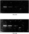
- the resulting image shown in FIG. 8A , was acquired and processed using an exposure time of 5 seconds and 4x4 binning. From FIG. 8A , one clearly visible band and one faintly visible band are detected in the blot. Also, a significant degree of background noise can be seen in the image at least partly as a result of the short exposure time.
- the blot was also imaged using high power laser illumination, a holographic diffuser having a 20-degree diffusing half angle, and the same image acquisition and processing parameters. The resulting high power laser image is shown in FIG. 8B , demonstrating a much lower level of background noise than seen with the LED illuminated of FIG. 8A .
- the signal intensity values calculated by the image processing software for FIGS. 8A and 8B were 16,978 and 1,218,723, respectively, representing a 72-fold improvement by replacing the LED epi-illumination with high power laser epi-illumination. Because of this large improvement in signal strength, the faint second band of FIG. 8A is much more pronounced in FIG. 8B , and an additional third band not visible with the LED epi-illumination of FIG. 8A is detected with the high power laser epi-illumination of FIG. 8B .
- the configuration produced double the signal intensity of an epi-illumination system that used the high power laser but with a fused silica optical diffuser.
- Such systems can include, for example, computer systems, cooling systems, optical systems of lenses and mirrors, power supplies, power regulators, and other elements enabling the operation of the apparatus.
Landscapes
- Physics & Mathematics (AREA)
- General Physics & Mathematics (AREA)
- Health & Medical Sciences (AREA)
- Optics & Photonics (AREA)
- Chemical & Material Sciences (AREA)
- Immunology (AREA)
- Life Sciences & Earth Sciences (AREA)
- Nuclear Medicine, Radiotherapy & Molecular Imaging (AREA)
- Analytical Chemistry (AREA)
- Biochemistry (AREA)
- General Health & Medical Sciences (AREA)
- Pathology (AREA)
- Chemical Kinetics & Catalysis (AREA)
- Investigating, Analyzing Materials By Fluorescence Or Luminescence (AREA)
Claims (12)
- Epi-illuminateur (400) pour un échantillon (402), l'épi-illuminateur (400) comprenant :une plateforme plane (401) ayant un côté échantillon configuré pour porter l'échantillon (402), le côté échantillon ayant une surface dans la plage de 10 cm2 à 500 cm2,une source de lumière d'excitation (403) comprenant un laser (404) et un diffuseur optique (405), la source de lumière d'excitation (403) étant configurée pour illuminer la surface du côté échantillon de la plateforme plane avec une intensité sensiblement uniforme, le diffuseur optique (405) étant monté au-dessus de la plateforme plane (401) et positionné entre le laser (404) et la plateforme plane (401) le long d'un chemin optique (406) du laser (404), le laser (404) ayant une puissance dans la plage de 5 W à 500 W, etun capteur (408) configuré pour détecter de la lumière d'émission de fluorescence (409) émettant à partir de l'échantillon (402), la lumière d'émission de fluorescence (409) ayant une longueur d'onde d'émission de fluorescence, et la lumière d'excitation n'ayant pas de longueur d'onde particulière de lumière associée aux émissions de fluorescence à partir de l'échantillon,caractérisé en ce que le laser (404) comprend une pluralité de modes spatiaux, chaque mode spatial a un motif particulier de rayon, et les différents modes spatiaux sont choisis spécifiquement parmi la pluralité de modes spatiaux et configurés pour produire une illumination combinée qui est spatialement incohérente.
- Epi-illuminateur (400) selon la revendication 1, le diffuseur optique étant un diffuseur holographique comprenant des motifs holographiques préparés incrustés dans son matériau de surface et caractérisé par un demi-angle de diffusion dans une plage de 3 degrés à 70 degrés, le demi-angle de diffusion étant défini par l'angle d'observation auquel une luminance a la moitié de la valeur de la luminance de lumière diffusée à l'angle 0°, avec une incidence perpendiculaire de lumière.
- Epi-illuminateur (400) selon la revendication 1 ou 2, le diffuseur optique (405) étant un diffuseur à verre dépoli ou une structure préparée à microlentilles.
- Epi-illuminateur (400) selon l'une des revendications 1 à 3, le laser (404) ayant une puissance dans la plage de 10 W à 80 W.
- Epi-illuminateur (400) selon l'une des revendications 1 à 4, le laser (404) étant une structure de laser semi-conducteur à émission par la surface et à cavité verticale (VCSEL) ou une structure de laser semi-conducteur à émission sur la limite de bande.
- Epi-illuminateur (400) selon l'une des revendications 1 à 5, la lumière d'excitation ayant une longueur d'onde dans la plage de 640 nm à 850 nm.
- Epi-illuminateur (400) selon l'une des revendications 1 à 6, la source de lumière d'excitation (403) comprenant deux ou plus de lasers (404) ou structures de laser et chacun des deux ou plus de lasers (404) ou structures de laser ayant une puissance dans la plage de 5 à 500 W.
- Epi-illuminateur (400) pour un échantillon (402), l'épi-illuminateur (400) comprenant :une plateforme plane (401) ayant un côté échantillon configuré pour porter l'échantillon (402), le côté échantillon ayant une surface dans la plage de 10 cm2 à 500 cm2,une source de lumière d'excitation (403) montée au-dessus de la plateforme plane (401), la source de lumière d'excitation (403) étant configurée pour illuminer la surface du côté échantillon de la plateforme plane avec une intensité sensiblement uniforme, la source de lumière d'excitation (403) comprenant cinq ou plus de lasers (404), et la source de lumière d'excitation (403) ayant une puissance totale de plus que 5 W, etun capteur (408) configuré pour détecter de la lumière d'émission de fluorescence (409) émettant à partir de l'échantillon (402), la lumière d'émission de fluorescence (409) ayant une longueur d'onde d'émission de fluorescence, et la lumière d'excitation n'ayant pas de longueur d'onde particulière de lumière associée aux émissions de fluorescence à partir de l'échantillon,caractérisé en ce que chacun des cinq ou plus de laser (404) comprend une pluralité de modes spatiaux, chaque mode spatial a un motif particulier de rayon, et les différents modes spatiaux sont choisis spécifiquement parmi la pluralité de modes spatiaux et configurés pour produire une illumination combinée qui est spatialement incohérente.
- Epi-illuminateur (400) selon la revendication 8, la source de lumière d'excitation (403) comprenant 100 ou plus de lasers (404) et chacun des 100 ou plus de lasers (404) est un laser semi-conducteur à émission sur la limite de bande.
- Epi-illuminateur (400) selon la revendication 8 ou 9, la source de lumière d'excitation (403) étant une structure de laser semi-conducteur VCSEL ou chacun de lasers (404) étant une structure de laser semi-conducteur à émission sur la limite de bande.
- Epi-illuminateur (400) selon l'une des revendications 8 à 10, chacun des lasers (404) ayant une puissance dans la plage de 5 W à 50 W.
- Procédé pour former une image d'un échantillon (402), le procédé comprenant :mettre à disposition l'épi-illuminateur (400) selon l'une des revendications 1 à 11, placer l'échantillon (402) sur la plateforme (plane (401),illuminer l'échantillon (402) avec de la lumière produite par la source de lumière d'excitation (403), et détecter, en utilisant le capteur (408), de la lumière d'émission de fluorescence (409) émettant à partir de l'échantillon (402).
Applications Claiming Priority (2)
| Application Number | Priority Date | Filing Date | Title |
|---|---|---|---|
| US201762553712P | 2017-09-01 | 2017-09-01 | |
| PCT/US2018/047701 WO2019046091A2 (fr) | 2017-09-01 | 2018-08-23 | Lasers à haute puissance pour transfert western |
Publications (3)
| Publication Number | Publication Date |
|---|---|
| EP3676598A2 EP3676598A2 (fr) | 2020-07-08 |
| EP3676598A4 EP3676598A4 (fr) | 2021-05-05 |
| EP3676598B1 true EP3676598B1 (fr) | 2024-10-02 |
Family
ID=65518610
Family Applications (1)
| Application Number | Title | Priority Date | Filing Date |
|---|---|---|---|
| EP18850493.0A Active EP3676598B1 (fr) | 2017-09-01 | 2018-08-23 | Lasers à haute puissance pour transfert western |
Country Status (4)
| Country | Link |
|---|---|
| US (1) | US10634614B2 (fr) |
| EP (1) | EP3676598B1 (fr) |
| CN (1) | CN111094938B (fr) |
| WO (1) | WO2019046091A2 (fr) |
Families Citing this family (1)
| Publication number | Priority date | Publication date | Assignee | Title |
|---|---|---|---|---|
| US20260225275A1 (en) * | 2025-02-04 | 2026-08-06 | Planet Earth Razors Ab | Wax-coated razor blades |
Family Cites Families (15)
| Publication number | Priority date | Publication date | Assignee | Title |
|---|---|---|---|---|
| US5143854A (en) | 1989-06-07 | 1992-09-01 | Affymax Technologies N.V. | Large scale photolithographic solid phase synthesis of polypeptides and receptor binding screening thereof |
| US6672739B1 (en) * | 1999-08-30 | 2004-01-06 | International Business Machines Corp. | Laser beam homogenizer |
| US7569130B2 (en) | 2002-01-24 | 2009-08-04 | University Tecnologies International Inc. | Fluorescent detection of proteins in polyacrylamide gels |
| US6970240B2 (en) | 2003-03-10 | 2005-11-29 | Applera Corporation | Combination reader |
| US20060018355A1 (en) | 2004-07-23 | 2006-01-26 | Comlasc.Nt-Ab | Laser diode arrays with reduced heat induced strain and stress |
| EP2264512B1 (fr) * | 2004-11-24 | 2014-06-04 | Battelle Memorial Institute | Procédé et appareil pour la détection de cellules rares |
| US7700928B2 (en) * | 2007-01-25 | 2010-04-20 | Etaluma, Inc. | Apparatus and method for interleaving detection of fluorescence and luminescence |
| EP2225600A2 (fr) * | 2007-09-05 | 2010-09-08 | Chroma Technology Corporation | Source de lumière |
| JP5062603B2 (ja) | 2010-07-29 | 2012-10-31 | 旭化成株式会社 | テレビ受信装置及び面光源装置 |
| US8743923B2 (en) * | 2012-01-31 | 2014-06-03 | Flir Systems Inc. | Multi-wavelength VCSEL array to reduce speckle |
| US8804280B2 (en) | 2012-02-03 | 2014-08-12 | Seagate Technology Llc | Actively synchronizing magnetic responses of a shield and a write pole |
| WO2013130183A1 (fr) * | 2012-02-29 | 2013-09-06 | Bio-Rad Laboratories, Inc. | Épi-illumination uniforme d'échantillons plans |
| JP6090875B2 (ja) * | 2013-06-04 | 2017-03-08 | Necディスプレイソリューションズ株式会社 | 照明光学系及びプロジェクタ |
| IL234766A (en) * | 2014-09-21 | 2015-09-24 | Visionsense Ltd | Fluorescent Imaging System |
| US10551608B2 (en) * | 2016-03-24 | 2020-02-04 | Molecular Devices, Llc | Imaging system with ancillary image detector for sample location |
-
2018
- 2018-08-23 EP EP18850493.0A patent/EP3676598B1/fr active Active
- 2018-08-23 WO PCT/US2018/047701 patent/WO2019046091A2/fr not_active Ceased
- 2018-08-23 CN CN201880056181.6A patent/CN111094938B/zh active Active
- 2018-08-23 US US16/110,333 patent/US10634614B2/en active Active
Also Published As
| Publication number | Publication date |
|---|---|
| WO2019046091A3 (fr) | 2020-03-26 |
| CN111094938B (zh) | 2024-09-03 |
| EP3676598A4 (fr) | 2021-05-05 |
| WO2019046091A2 (fr) | 2019-03-07 |
| CN111094938A (zh) | 2020-05-01 |
| US10634614B2 (en) | 2020-04-28 |
| US20190072490A1 (en) | 2019-03-07 |
| EP3676598A2 (fr) | 2020-07-08 |
Similar Documents
| Publication | Publication Date | Title |
|---|---|---|
| US7145645B2 (en) | Imaging of biological samples using electronic light detector | |
| ES2635094T3 (es) | Procedimientos y aparatos para la formación confocal de imágenes | |
| CN102016546B (zh) | 用于多表面成像的补偿器 | |
| US7551271B2 (en) | Uncaging devices | |
| US20030151735A1 (en) | Scanning of biological samples | |
| JP7003241B2 (ja) | 貼り付けスライド判定システム | |
| JP2002508857A (ja) | 暗視野の照射のための光学的キャビティを用いる標本照射装置および使用方法 | |
| US20080265139A1 (en) | Combination reader | |
| JP2009526997A (ja) | 複数のソースからの光学信号をリアルタイムで同時に監視する方法及びシステム | |
| JP2003527598A (ja) | 試験物質中の有機分子の検出のための装置及び方法 | |
| US20050092934A1 (en) | Fluorescence microscope and observation method using the same | |
| US20030133009A1 (en) | System and method for detecting with high resolution a large, high content field | |
| TWI263072B (en) | Method and system for reading microarrays | |
| US20020005493A1 (en) | Optical components for microarray analysis | |
| US20090292479A1 (en) | Method for analyzing image from bio-detection analyzer | |
| EP2893323A1 (fr) | Systèmes et procédé pour imagerie à fluorescence | |
| US10634614B2 (en) | High powered lasers for western blotting | |
| WO2003085387A1 (fr) | Dispositif de detection d'une epifluorescence induite par laser | |
| US6762840B1 (en) | Image information reading apparatus designed to maintain light amount to be detected at uniform level | |
| US20250283169A1 (en) | Enhanced resolution imaging | |
| CA2450385C (fr) | Correction de champ plat d'images bidimensionnelles d'essais biochimiques | |
| US20080253409A1 (en) | Multi-Channel Bio-Chip Scanner | |
| US20250377524A1 (en) | Novel illumination and background rejection for enhanced resolution imaging | |
| KR20250034411A (ko) | 시퀀싱 시스템에서 신호 변동의 감소를 위한 장치 | |
| JP4898793B2 (ja) | 検出器中の半径方向の勾配を補うために再配分される入射光 |
Legal Events
| Date | Code | Title | Description |
|---|---|---|---|
| STAA | Information on the status of an ep patent application or granted ep patent |
Free format text: STATUS: THE INTERNATIONAL PUBLICATION HAS BEEN MADE |
|
| PUAI | Public reference made under article 153(3) epc to a published international application that has entered the european phase |
Free format text: ORIGINAL CODE: 0009012 |
|
| STAA | Information on the status of an ep patent application or granted ep patent |
Free format text: STATUS: REQUEST FOR EXAMINATION WAS MADE |
|
| 17P | Request for examination filed |
Effective date: 20200228 |
|
| AK | Designated contracting states |
Kind code of ref document: A2 Designated state(s): AL AT BE BG CH CY CZ DE DK EE ES FI FR GB GR HR HU IE IS IT LI LT LU LV MC MK MT NL NO PL PT RO RS SE SI SK SM TR |
|
| AX | Request for extension of the european patent |
Extension state: BA ME |
|
| DAV | Request for validation of the european patent (deleted) | ||
| DAX | Request for extension of the european patent (deleted) | ||
| RAP3 | Party data changed (applicant data changed or rights of an application transferred) |
Owner name: BIO-RAD LABORATORIES, INC. |
|
| A4 | Supplementary search report drawn up and despatched |
Effective date: 20210406 |
|
| RIC1 | Information provided on ipc code assigned before grant |
Ipc: G01N 21/64 20060101AFI20210329BHEP Ipc: G02B 5/02 20060101ALI20210329BHEP Ipc: G02B 21/16 20060101ALN20210329BHEP |
|
| STAA | Information on the status of an ep patent application or granted ep patent |
Free format text: STATUS: EXAMINATION IS IN PROGRESS |
|
| 17Q | First examination report despatched |
Effective date: 20230123 |
|
| GRAP | Despatch of communication of intention to grant a patent |
Free format text: ORIGINAL CODE: EPIDOSNIGR1 |
|
| STAA | Information on the status of an ep patent application or granted ep patent |
Free format text: STATUS: GRANT OF PATENT IS INTENDED |
|
| RIC1 | Information provided on ipc code assigned before grant |
Ipc: G02B 21/16 20060101ALN20240313BHEP Ipc: G02B 5/02 20060101ALI20240313BHEP Ipc: G01N 21/64 20060101AFI20240313BHEP |
|
| INTG | Intention to grant announced |
Effective date: 20240327 |
|
| GRAS | Grant fee paid |
Free format text: ORIGINAL CODE: EPIDOSNIGR3 |
|
| GRAA | (expected) grant |
Free format text: ORIGINAL CODE: 0009210 |
|
| STAA | Information on the status of an ep patent application or granted ep patent |
Free format text: STATUS: THE PATENT HAS BEEN GRANTED |
|
| P01 | Opt-out of the competence of the unified patent court (upc) registered |
Free format text: CASE NUMBER: APP_43968/2024 Effective date: 20240729 |
|
| AK | Designated contracting states |
Kind code of ref document: B1 Designated state(s): AL AT BE BG CH CY CZ DE DK EE ES FI FR GB GR HR HU IE IS IT LI LT LU LV MC MK MT NL NO PL PT RO RS SE SI SK SM TR |
|
| REG | Reference to a national code |
Ref country code: GB Ref legal event code: FG4D |
|
| REG | Reference to a national code |
Ref country code: CH Ref legal event code: EP |
|
| REG | Reference to a national code |
Ref country code: DE Ref legal event code: R096 Ref document number: 602018075039 Country of ref document: DE |
|
| REG | Reference to a national code |
Ref country code: IE Ref legal event code: FG4D |
|
| REG | Reference to a national code |
Ref country code: LT Ref legal event code: MG9D |
|
| REG | Reference to a national code |
Ref country code: NL Ref legal event code: MP Effective date: 20241002 |
|
| REG | Reference to a national code |
Ref country code: AT Ref legal event code: MK05 Ref document number: 1728826 Country of ref document: AT Kind code of ref document: T Effective date: 20241002 |
|
| PG25 | Lapsed in a contracting state [announced via postgrant information from national office to epo] |
Ref country code: NL Free format text: LAPSE BECAUSE OF FAILURE TO SUBMIT A TRANSLATION OF THE DESCRIPTION OR TO PAY THE FEE WITHIN THE PRESCRIBED TIME-LIMIT Effective date: 20241002 |
|
| PG25 | Lapsed in a contracting state [announced via postgrant information from national office to epo] |
Ref country code: NL Free format text: LAPSE BECAUSE OF FAILURE TO SUBMIT A TRANSLATION OF THE DESCRIPTION OR TO PAY THE FEE WITHIN THE PRESCRIBED TIME-LIMIT Effective date: 20241002 |
|
| PG25 | Lapsed in a contracting state [announced via postgrant information from national office to epo] |
Ref country code: HR Free format text: LAPSE BECAUSE OF FAILURE TO SUBMIT A TRANSLATION OF THE DESCRIPTION OR TO PAY THE FEE WITHIN THE PRESCRIBED TIME-LIMIT Effective date: 20241002 Ref country code: PT Free format text: LAPSE BECAUSE OF FAILURE TO SUBMIT A TRANSLATION OF THE DESCRIPTION OR TO PAY THE FEE WITHIN THE PRESCRIBED TIME-LIMIT Effective date: 20250203 Ref country code: IS Free format text: LAPSE BECAUSE OF FAILURE TO SUBMIT A TRANSLATION OF THE DESCRIPTION OR TO PAY THE FEE WITHIN THE PRESCRIBED TIME-LIMIT Effective date: 20250202 |
|
| PG25 | Lapsed in a contracting state [announced via postgrant information from national office to epo] |
Ref country code: FI Free format text: LAPSE BECAUSE OF FAILURE TO SUBMIT A TRANSLATION OF THE DESCRIPTION OR TO PAY THE FEE WITHIN THE PRESCRIBED TIME-LIMIT Effective date: 20241002 |
|
| PG25 | Lapsed in a contracting state [announced via postgrant information from national office to epo] |
Ref country code: BG Free format text: LAPSE BECAUSE OF FAILURE TO SUBMIT A TRANSLATION OF THE DESCRIPTION OR TO PAY THE FEE WITHIN THE PRESCRIBED TIME-LIMIT Effective date: 20241002 |
|
| PG25 | Lapsed in a contracting state [announced via postgrant information from national office to epo] |
Ref country code: ES Free format text: LAPSE BECAUSE OF FAILURE TO SUBMIT A TRANSLATION OF THE DESCRIPTION OR TO PAY THE FEE WITHIN THE PRESCRIBED TIME-LIMIT Effective date: 20241002 |
|
| PG25 | Lapsed in a contracting state [announced via postgrant information from national office to epo] |
Ref country code: NO Free format text: LAPSE BECAUSE OF FAILURE TO SUBMIT A TRANSLATION OF THE DESCRIPTION OR TO PAY THE FEE WITHIN THE PRESCRIBED TIME-LIMIT Effective date: 20250102 |
|
| PG25 | Lapsed in a contracting state [announced via postgrant information from national office to epo] |
Ref country code: AT Free format text: LAPSE BECAUSE OF FAILURE TO SUBMIT A TRANSLATION OF THE DESCRIPTION OR TO PAY THE FEE WITHIN THE PRESCRIBED TIME-LIMIT Effective date: 20241002 Ref country code: LV Free format text: LAPSE BECAUSE OF FAILURE TO SUBMIT A TRANSLATION OF THE DESCRIPTION OR TO PAY THE FEE WITHIN THE PRESCRIBED TIME-LIMIT Effective date: 20241002 Ref country code: GR Free format text: LAPSE BECAUSE OF FAILURE TO SUBMIT A TRANSLATION OF THE DESCRIPTION OR TO PAY THE FEE WITHIN THE PRESCRIBED TIME-LIMIT Effective date: 20250103 |
|
| PG25 | Lapsed in a contracting state [announced via postgrant information from national office to epo] |
Ref country code: CZ Free format text: LAPSE BECAUSE OF FAILURE TO SUBMIT A TRANSLATION OF THE DESCRIPTION OR TO PAY THE FEE WITHIN THE PRESCRIBED TIME-LIMIT Effective date: 20241002 Ref country code: PL Free format text: LAPSE BECAUSE OF FAILURE TO SUBMIT A TRANSLATION OF THE DESCRIPTION OR TO PAY THE FEE WITHIN THE PRESCRIBED TIME-LIMIT Effective date: 20241002 |
|
| PG25 | Lapsed in a contracting state [announced via postgrant information from national office to epo] |
Ref country code: RS Free format text: LAPSE BECAUSE OF FAILURE TO SUBMIT A TRANSLATION OF THE DESCRIPTION OR TO PAY THE FEE WITHIN THE PRESCRIBED TIME-LIMIT Effective date: 20250102 |
|
| PG25 | Lapsed in a contracting state [announced via postgrant information from national office to epo] |
Ref country code: SM Free format text: LAPSE BECAUSE OF FAILURE TO SUBMIT A TRANSLATION OF THE DESCRIPTION OR TO PAY THE FEE WITHIN THE PRESCRIBED TIME-LIMIT Effective date: 20241002 |
|
| REG | Reference to a national code |
Ref country code: DE Ref legal event code: R097 Ref document number: 602018075039 Country of ref document: DE |
|
| PG25 | Lapsed in a contracting state [announced via postgrant information from national office to epo] |
Ref country code: DK Free format text: LAPSE BECAUSE OF FAILURE TO SUBMIT A TRANSLATION OF THE DESCRIPTION OR TO PAY THE FEE WITHIN THE PRESCRIBED TIME-LIMIT Effective date: 20241002 |
|
| PG25 | Lapsed in a contracting state [announced via postgrant information from national office to epo] |
Ref country code: EE Free format text: LAPSE BECAUSE OF FAILURE TO SUBMIT A TRANSLATION OF THE DESCRIPTION OR TO PAY THE FEE WITHIN THE PRESCRIBED TIME-LIMIT Effective date: 20241002 |
|
| PG25 | Lapsed in a contracting state [announced via postgrant information from national office to epo] |
Ref country code: RO Free format text: LAPSE BECAUSE OF FAILURE TO SUBMIT A TRANSLATION OF THE DESCRIPTION OR TO PAY THE FEE WITHIN THE PRESCRIBED TIME-LIMIT Effective date: 20241002 |
|
| PG25 | Lapsed in a contracting state [announced via postgrant information from national office to epo] |
Ref country code: SK Free format text: LAPSE BECAUSE OF FAILURE TO SUBMIT A TRANSLATION OF THE DESCRIPTION OR TO PAY THE FEE WITHIN THE PRESCRIBED TIME-LIMIT Effective date: 20241002 |
|
| PG25 | Lapsed in a contracting state [announced via postgrant information from national office to epo] |
Ref country code: IT Free format text: LAPSE BECAUSE OF FAILURE TO SUBMIT A TRANSLATION OF THE DESCRIPTION OR TO PAY THE FEE WITHIN THE PRESCRIBED TIME-LIMIT Effective date: 20241002 |
|
| PLBE | No opposition filed within time limit |
Free format text: ORIGINAL CODE: 0009261 |
|
| STAA | Information on the status of an ep patent application or granted ep patent |
Free format text: STATUS: NO OPPOSITION FILED WITHIN TIME LIMIT |
|
| PG25 | Lapsed in a contracting state [announced via postgrant information from national office to epo] |
Ref country code: SE Free format text: LAPSE BECAUSE OF FAILURE TO SUBMIT A TRANSLATION OF THE DESCRIPTION OR TO PAY THE FEE WITHIN THE PRESCRIBED TIME-LIMIT Effective date: 20241002 |
|
| 26N | No opposition filed |
Effective date: 20250703 |
|
| PGFP | Annual fee paid to national office [announced via postgrant information from national office to epo] |
Ref country code: DE Payment date: 20250827 Year of fee payment: 8 |
|
| PGFP | Annual fee paid to national office [announced via postgrant information from national office to epo] |
Ref country code: GB Payment date: 20250826 Year of fee payment: 8 |
|
| PGFP | Annual fee paid to national office [announced via postgrant information from national office to epo] |
Ref country code: FR Payment date: 20250825 Year of fee payment: 8 |
|
| REG | Reference to a national code |
Ref country code: CH Ref legal event code: H13 Free format text: ST27 STATUS EVENT CODE: U-0-0-H10-H13 (AS PROVIDED BY THE NATIONAL OFFICE) Effective date: 20260324 |
|
| PG25 | Lapsed in a contracting state [announced via postgrant information from national office to epo] |
Ref country code: MC Free format text: LAPSE BECAUSE OF FAILURE TO SUBMIT A TRANSLATION OF THE DESCRIPTION OR TO PAY THE FEE WITHIN THE PRESCRIBED TIME-LIMIT Effective date: 20241002 |
|
| PG25 | Lapsed in a contracting state [announced via postgrant information from national office to epo] |
Ref country code: LU Free format text: LAPSE BECAUSE OF NON-PAYMENT OF DUE FEES Effective date: 20250823 |
|
| PG25 | Lapsed in a contracting state [announced via postgrant information from national office to epo] |
Ref country code: CH Free format text: LAPSE BECAUSE OF NON-PAYMENT OF DUE FEES Effective date: 20250831 |
|
| REG | Reference to a national code |
Ref country code: BE Ref legal event code: MM Effective date: 20250831 |
|
| PG25 | Lapsed in a contracting state [announced via postgrant information from national office to epo] |
Ref country code: LT Free format text: LAPSE BECAUSE OF FAILURE TO SUBMIT A TRANSLATION OF THE DESCRIPTION OR TO PAY THE FEE WITHIN THE PRESCRIBED TIME-LIMIT Effective date: 20241002 |
|
| PG25 | Lapsed in a contracting state [announced via postgrant information from national office to epo] |
Ref country code: BE Free format text: LAPSE BECAUSE OF NON-PAYMENT OF DUE FEES Effective date: 20250831 Ref country code: IE Free format text: LAPSE BECAUSE OF NON-PAYMENT OF DUE FEES Effective date: 20250823 |